

1/8
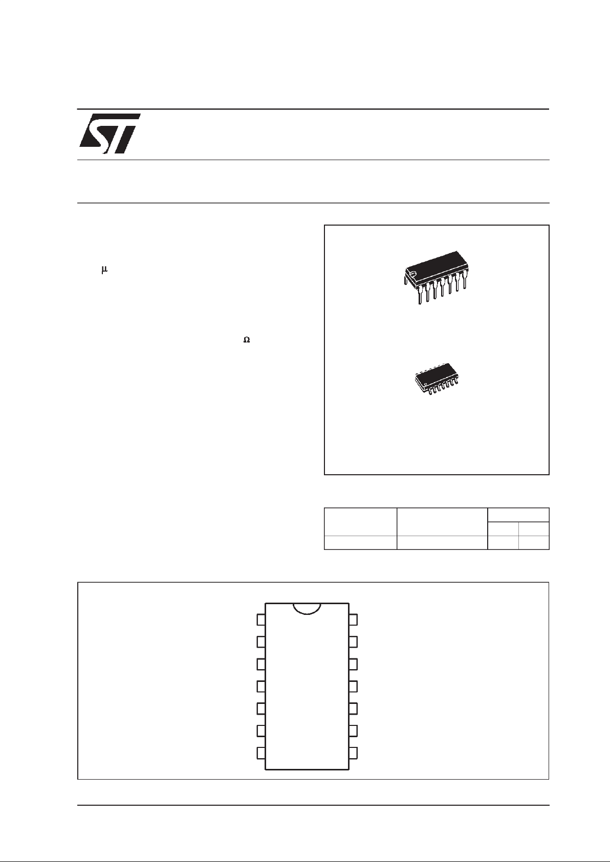
TS3V556
N
DIP14
(Plastic Package)
D
SO14
.DEDICATEDTO3.3VORBATTERY SUPPLY
(Specified at 3V and 5V)
.VERY LOW POWERCONSUMPTION :
90 A/tim at VCC=3V
.WIDE SINGLE SUPPLY RANGE :
+2.7V to +16V
.HIGH OUTPUT CURRENTCAPABILITY
.SUPPLY CURRENT SPIKES REDUCED
DURING OUTPUT TRANSITIONS
.HIGH INPUT IMPEDANCE: 10
12
.PIN-TO-PIN AND FUNCTIONALLY COMPATI-
BLE WITH BIPOLAR NE556 AND CMOS
TS556
.OUTPUT COMPATIBLE WITH TTL,CMOS
AND LOGIC MOS
DESCRIPTION
The TS3V556 with its low consumption (90µA/tim
at VCC= 3V) is a dual CMOS timer dedicated to
3.3Vor batterysupply(specified at 3Vand5Voffering also a highfrequency (f
(max)
2MHz at VCC=3V
and 2.7 MHz at VCC= 5V). Thus, either in monostable or astable mode, timing remains very accurate.
Timing capacitors can also be minimized due to
high input impedance (1012Ω).
ORDER CODES
Part Number
Temperature
Range
Package
ND
TS3V556I -40, +125
o
C ll
3V LOW POWER DUAL TIMERS
Trigger
Output
Control Voltage
4
8
5
6
7
9
10
11
12
13
14
Trigger
Thresho ld
Discharge
Re s e t
Output
Discharge
GND
1
2
3
Thre shold
Control Voltage
Rese t
CC
V
PIN CONNECTIONS (top view)
May 2000
TS3V556
2/8
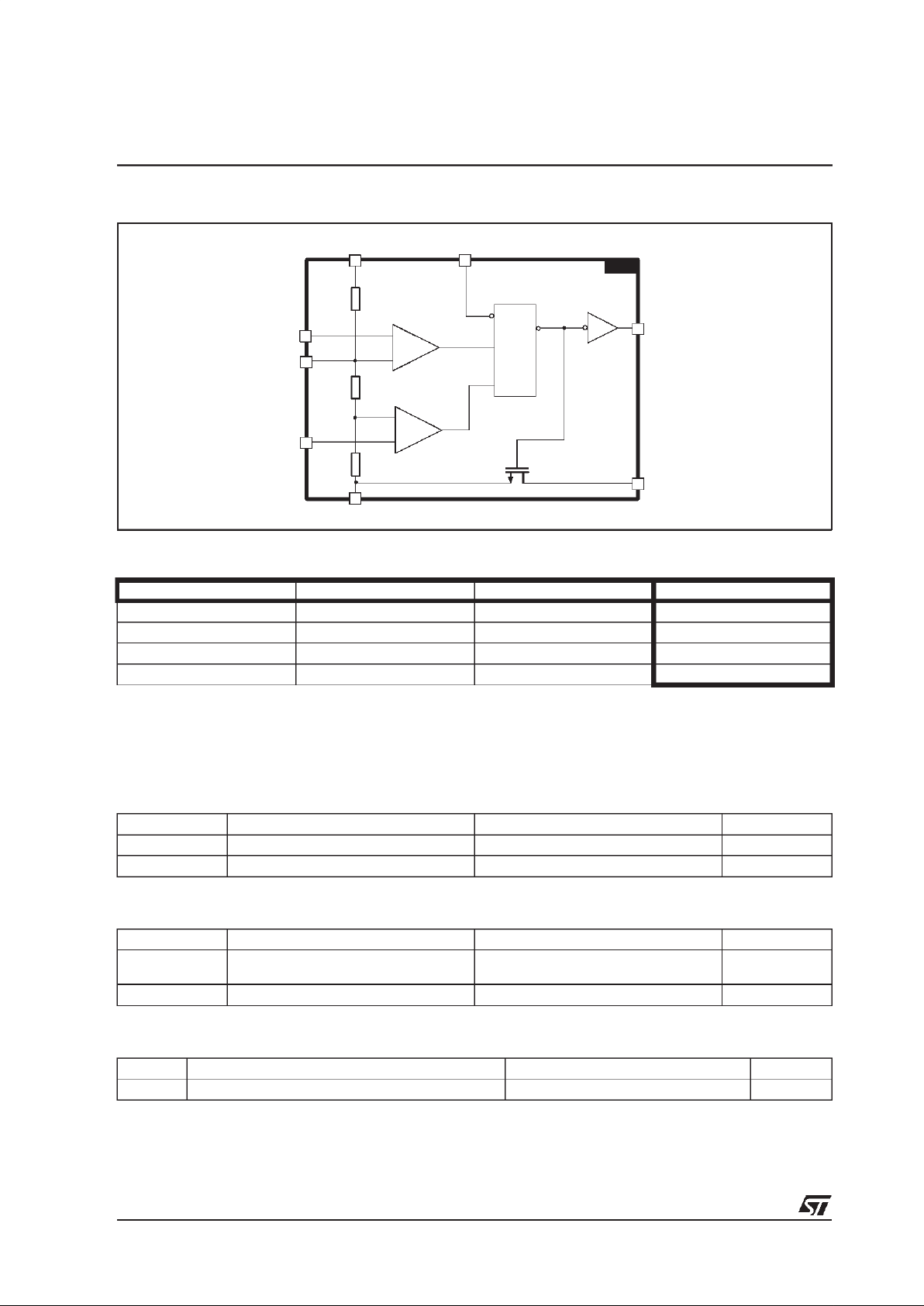
FUNCTION TABLE
RESET TRIGGER THRESHOLD OUTPUT
Low x x Low
High Low x High
High High High Low
High High Low Previous State
LOW
Level Voltage ≤ Min voltage specified
HIGH
Level Voltage ≥ Max voltage specified
X
Irrelevant
ABSOLUTE MAXIMUM RATINGS
Symbol Parameter Value Unit
V
CC
Supply Voltage +18 V
T
J
Junction Temperature +150
o
C
THERMAL CHARACTERISTICS
Symbol Parameter Value Unit
T
oper
Operating TemperatureRange
TS3V556I,AI -40 to +125
o
C
T
stg
Storage Temperature Range -65 to +150
o
C
Output
Discharge
Ground
Trigger
Control
Voltage
Threshold
V
CC
Reset
R
R
R
B
A
R1
R
S
Q
+
-
+
-
4/10
5/9
14
2/12
3/11
6/8
7
1/13
3V556
BLOCK DIAGRAM (1/2 TS3V556)
OPERATING CONDITIONS
Symbol Parameter Value Unit
V
CC
Supply Voltage +2.7 to +16 V
TS3V556
3/8
ELECTRICAL CHARACTERISTICS
VCC= +3V , T
amb
= +25oC , Reset to VCC(unless otherwise specified)
STATIC
Symbol Parameter
TS3V556I
Unit
Min. Typ. Max.
I
CC
Supply Current - (no load, High and Low States, per
timer)
T
amb
= +25oC
T
min.
T
amb Tmax
.
90 230
230
µA
V
CL
Control Voltage
T
amb
= +25oC
T
min.
T
amb Tmax
.
1.8
1.7
2 2.2
2.3
V
V
DIS
Discharge Saturation Voltage (I
DIS
= 1mA)
T
amb
= +25oC
T
min.
T
amb Tmax
.
0.05
-
0.2
0.25
V
V
OL
Low Level Output Voltage (I
SINK
= 1mA)
T
amb
= +25oC
T
min.
T
amb Tmax
.
0.1 0.3
0.35
V
V
OH
High Level Output Voltage (I
SOURCE
= -0.3mA)
T
amb
= +25oC
T
min.
T
amb Tmax
.
2.5
2.5
2.9
V
V
TRIG
Trigger Voltage
T
amb
= +25oC
T
min.
T
amb Tmax
.
0.9
0.8
1 1.1
1.2
V
I
TRIG
Trigger Current 10 pA
I
TH
Threshold Current 10 pA
V
RESET
Reset Voltage
T
amb
= +25°C
T
min
. T
amb Tmax.
0.4
0.3
1.1 1.5
2.0
V
I
RESET
Reset Current 10 pA
I
DIS
Discharge Pin Leakage Current 1 100 nA
DYNAMIC
Symbol Parameter
TS3V556I
Unit
Min. Typ. Max.
Timing Accuracy (Monostable)
R = 10kΩ , C = 0.1µF - (note 1)
1
%
Timing Shift with supply voltage variations (Monostable)
R = 10kΩ , C = 0.1µF, V
CC
= +3V +/-0.3V - (note 1)
0.5
%/V
Timing Shift with temperature - (note 1)
T
min. Tamb Tmax
.75
ppm/°
C
fmax Maximum astable frequency - (note 2)
R
A
= 470Ω ,RB= 200Ω, C = 200pF
2
MHz
Astable frequency accuracy - (note 2)
R
A=RB
=1kΩto 100kΩ,C=0.1µF
5
%
Timing Shift with supply voltage variations (Astable mode) - (note
2)
R
A=RB
= 10kΩ, C = 0.1µF, VCC= +3 to+5V
0.5
%/V
t
r
Output Rise Time(C
LOAD
= 10pF) 25 ns
t
f
Output Fall Time (C
LOAD
= 10pF) 20 ns
t
PD
Trigger Propagation Delay 100 ns
t
RPW
Minimum Reset Pulse Width (V
TRIG
= +3V) 350 ns
Note : 1. See Figure 2
2. See Figure 4

TS3V556
4/8
ELECTRICAL CHARACTERISTICS
VCC= +5V , T
amb
= +25oC , Reset to VCC(unless otherwise specified)
STATIC
Symbol Parameter
TS3V556I
Unit
Min. Typ. Max.
I
CC
Supply Current - (no load, High and Low States, per
timer)
T
amb
= +25°C
T
min
. T
amb Tmax
.
110 250
250
µA
V
CL
Control Voltage
T
amb
= +25°C
T
min
. T
amb Tmax
.
2.9
2.8
3.3 3.8
3.9
V
V
DIS
Discharge Saturation Voltage (I
DIS
= 10mA)
T
amb
= +25°C
T
min
. T
amb Tmax
.
0.2 0.3
0.35
V
V
OL
Low Level Output Voltage (I
SINK
= 8mA)
T
amb
= +25°C
T
min
. T
amb Tmax
.
0.3 0.6
0.8
V
V
OH
High Level Output Voltage (I
SOURCE
= -2mA)
T
amb
= +25°C
T
min
. T
amb Tmax
.
4.4
4.4
4.6
V
V
TRIG
Trigger Voltage
T
amb
= +25°C
T
min
. T
amb Tmax
.
1.36
1.26
1.67 1.96
2.06
V
I
TRIG
Trigger Current 10 pA
I
TH
Threshold Current 10 pA
V
RESET
Reset Voltage
T
amb
= +25°C
T
min
. T
amb Tmax
.
0.4
0.3
1.1 1.5
2.0
V
I
RESET
Reset Current 10 pA
I
DIS
Discharge Pin Leakage Current 1 100 nA
DYNAMIC
Symbol Parameter
TS3V556I
Unit
Min. Typ. Max.
Timing Accuracy (Monostable) - (note1)
R = 10kΩ , C = 0.1µF - (note 1)
2
%
Timing Shift with supply voltage variations (Monostable)- (note1)
R = 10kΩ , C = 0.1µF, V
CC
= +5V +/-1V
0.38
%/V
Timing Shift with temperature - (note1)
T
min .Tamb Tmax
.75
ppm/°
C
fmax Maximum astable frequency - (note 2)
R
A
= 470Ω ,RB= 200Ω, C = 200pF
2.7
MHz
Astable frequency accuracy - (note 2)
R
A=RB
=1kΩto 100kΩ,C=0.1µF
3
%
Timing Shift with supply voltage variations (Astable mode) - (note
2)
R
A=RB
= 10kΩ, C = 0.1µF, VCC= +5V to+12V
0.1
%/V
t
r
Output Rise Time (C
LOAD
= 10pF) 25 ns
t
f
Output Fall Time (C
LOAD
= 10pF) 20 ns
t
PD
Trigger Propagation Delay 100 ns
t
RPW
Minimum Reset Pulse Width (V
TRIG
= +5V) 350 ns
Note : 1. See Figure 2
2. See Figure 4

TS3V556
5/8
APPLICATION INFORMATION
MONOSTABLEOPERATION
In the monostable mode,the timer functions as a
one-shot. Referring to figure 2 the external capacitor is initially held discharged by a transistor inside
the timer.
V
CC
Reset
Trigger
Out
R
C
Control Voltage
0.01 F
µ
1/2
TS3V556
Figure 2
CAPACITORVOLTAGE = 2.0V/div
Ω
Ω
µ
t = 0.1ms / div
INPUT= 2.0V/div
OUTPUTVOLTAGE = 5.0V/div
R = 9.1k , C = 0.01 F , R = 1.0k
L
Figure 3
TYPICAL CHARACTERISTICS
CC
SUPPLYVOLTAGE,V (V)
CC
SUPPLY CURRENT, I ( A)
µ
300
200
100
0481216
Figure 1 : Supply Current (each timer)
versus supply voltage.
The circuittriggerson a negative-going inputsignal
whenthelevel reaches1/3VCC. Oncetriggered,the
circuit remains in this state until the set time has
elapsed,even if it is triggered again during this interval. The duration of the output HIGH state is
given by t = 1.1 R x C.
Notice that since the charge rate and the threshold
level of the comparator are both directly proportional to supply voltage, the timing interval is independent of supply. Applying a negative pulse
simultaneously to the Reset terminal (pin 4 or 10)
and theTriggerterminal (pin 2 or 8) during the timing cycle discharges the external capacitor and
causes thecycletostartover.The timingcyclenow
starts on the positive edge of the reset pulse. During the timethe reset pulseis applied, the outputis
driven to its LOW state.
When a negative triggerpulseisapplied to the trigger terminal, the flip-flop is set, releasing the short
circuit across theexternal capacitorand drivingthe
output HIGH. The voltage across the capacitor increasesexponentiallywiththetime constantτ=Rx
C.
When the voltage across the capacitor equals 2/3
VCC, the comparator resets the flip-flop which then
dischargesthecapacitorrapidlyand drivesthe output to its LOW state.
Figure 3 shows the actual waveformsgenerated in
this mode of operation.
When Reset is not used, it should be tied high to
avoid any possible or false triggering.

TS3V556
6/8
V
CC
Reset
Out
R
C
R
A
B
Control
Voltage
0.01 F
µ
TS3V556
Figure 4
ΩΩ
µ
t = 0.5 ms / div
OUTPUT VOLTAGE = 5.0V/div
CAPACITOR VOLTAGE= 1.0V/div
L
R = R = 4.8 k , C =0.1 F , R = 1.0k
AB
Figure 5
ASTABLE OPERATION
When the circuit is connected as shown in
figure 4 , it triggers itself and free runs as a
multivibrator. The exter nal c apac itor charges
throughRAandRBanddischargesthroughRBonly.
Thus the duty cyclemay be precisely set by the ratio of these two resistors.
In the astable mode of operation, C charges and
dischargesbetween 1/3VCCand 2/3VCC.As inthe
triggered mode, the charge and discharge times
and therefore frequency, are independent of the
supply voltage.
Figure5showsactualwaveformsgeneratedinthis
mode of operation.
The charge time (output HIGH) is given by :
t1 = 0.693 (RA+RB)C
and the discharge time (output LOW) by :
t2 = 0.693 (RB)C
Thus the total period T is given by :
T = t1 + t2 = 0.693 (RA+2RB)C
The frequency of oscillation is then :
f
TR R)C
B
==
+
1144
2
.
(
A
The duty cycle is given by : D
R
RR
=
+
B
AB
2

TS3V556
7/8
PACKAGE MECHANICAL DATA
14 PINS - PLASTIC DIP
Dimensions
Millimeters Inches
Min. Typ. Max. Min. Typ. Max.
a1 0.51 0.020
B 1.39 1.65 0.055 0.065
b 0.5 0.020
b1 0.25 0.010
D 20 0.787
E 8.5 0.335
e 2.54 0.100
e3 15.24 0.600
F 7.1 0.280
i 5.1 0.201
L 3.3 0.130
Z 1.27 2.54 0.050 0.100

TS3V556
8/8
nformation furnished is believedto beaccurate and reliable. However, STMicroelectronicsassumes noresponsibility forthe consequences ofuse of suchinformation nor forany infringementof patents or other rights ofthird parties whichmay result from its use.
No license is grantedby implicationor otherwise underany patentor patent rights of STMicroelectronics. Specifications mentioned
in this publication are subject to change without notice. This publication supersedes and replaces all information previously supplied. STMicroelectronicsproducts are not authorizedfor use ascritical components in lifesupport devices orsystems without express written approval of STMicroelectronics.
The ST logo is a trademark of STMicroelectronics
2000 STMicroelectronics – Printed in Italy – All Rights Reserved
STMicroelectronics GROUP OF COMPANIES
Australia - Brazil - China - Finland - France - Germany - Hong Kong - India - Italy - Japan - Malaysia - Malta- Morocco
Singapore - Spain - Sweden - Switzerland - UnitedKingdom - U.S.A.
http://www.st.com
PACKAGE MECHANICAL DATA
14 PINS - PLASTIC MICROPACKAGE (SO)
Dimensions
Millimeters Inches
Min. Typ. Max. Min. Typ. Max.
A 1.75 0.069
a1 0.1 0.2 0.004 0.008
a2 1.6 0.063
b 0.35 0.46 0.014 0.018
b1 0.19 0.25 0.007 0.010
C 0.5 0.020
c1 45
o
(typ.)
D 8.55 8.75 0.336 0.334
E 5.8 6.2 0.228 0.244
e 1.27 0.050
e3 7.62 0.300
F 3.8 4.0 0.150 0.157
G 4.6 5.3 0.181 0.208
L 0.5 1.27 0.020 0.050
M 0.68 0.027
S8
o
(max.)
 Loading...