

3V MICROPOWERQUAD VOLTAGE COMPARATORS
.
DEDICATED TO 3.3V ORBATTERY SUPPLY
(specifiedat 3V and 5V)
.
PUSH-PULL CMOS OUTPUT (NO EXTERNAL PULL-UP RESISTOR REQUIRED)
.
EXTREMELYLOW SUPPLYCURRENT :
7µAtyp / comparator
.
WIDESINGLESUPPLY RANGE
2.7V to 16V
.
EXTREMELYLOW INPUTCURRENTS :
1pA TYP
.
INPUT COMMON-MODE VOLTAGE RANGE
INCLUDESGND
.
FASTRESPONSETIME : 2µs typ for
5mV overdrive
.
PIN-TO-PINANDFUNCTIONALLY
COMPATIBLEWITH BIPOLARLM339
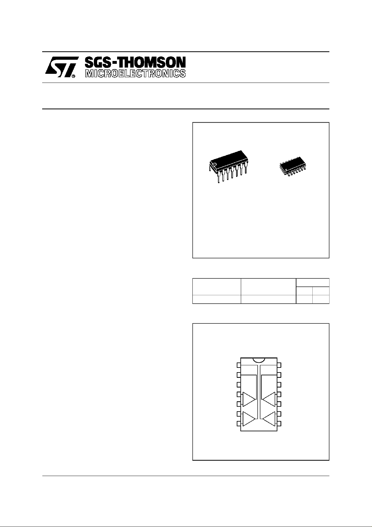
N
DIP14
(Plastic Package)
TS3V3704
D
SO14
(Plastic Micropackage)
DESCRIPTION
The TS3V3704is a micropowerquadCMOSvoltage comparatorwith extremelylow consumption
of 7µAtyp / comparator(20timeslessthanbipolar
LM339). The push-pull CMOSoutputstage allows
powerandspacesavingbyeliminatingtheexternal
pull-up resistor required by usual open-collector
output comparators.
Thus response times remain similarto the LM339.
ORDER CODES
Part Number
TS3V3704I -40
PIN CONNECTIONS (top view)
Output 2
1
Output 1
2
V
3
CC
Inverting Input 1
Non-invertingInput 1
Inverting Input2
Non-inverting Input 2
4
5
6
7
Temperature
Range
o
C, +125oC ●●
-
+-
-
+-
+
+
Package
14+Output 3
13
Output 4
-
V
12
CC
11
Non-inverting Input 4
Inverting Input 4
10
9
Non-inverting Input 3
Inverting Input 3
8
ND
October 1997
1/6

TS3V3704
SCHEMATIC DIAGRAM (for 1/4 TS3V3704)
T
1
T
2
T
9
V+
CC
T
10
T
17
R
1
Input- Input+
TT
34
T
8
T
5
T
6
T
7
T
11
TT
14 15
T
12
T
13
T
16
V-
CC
TT
18 21
Output
TT
19 20
MAXIMUMRATINGS
Symbol Parameter Value Unit
+
V
V
V
T
T
Notes : 1. All voltage values, except differential voltage,are withrespect to network ground terminal.
Supply Voltage- (note 1) 18 V
CC
Differential Input Voltage - (note 2) ±18 V
id
Input Voltage- (note 3) 18 V
V
i
Output Voltage 18 V
O
Output Current 20 mA
I
O
Operating Free-Air TemperatureRange
oper
Storage TemperatureRange -65 to +150
stg
2. Differential voltages are the non-inverting input terminalwith respect to the inverting input terminal.
3. The magnitude of the input andthe output voltages must never exceedthe magnitudeof thepositive supply voltage.
4. Short circuit from outputs to V
+
can cause excessive heating and eventualdestruction.
CC
TS3V3704I -40 to +125
o
C
o
C
OPERATINGCONDITIONS
Symbol Parameter Value Unit
+
V
V
2/6
Supply Voltage 2.7 to 16 V
CC
Common Mode Input VoltageRange 0 to V
icm
CC
+
-1.5 V

TS3V3704
ELECTRICAL CHARACTERISTICS
+
= 3V, V
V
CC
Symbol Parameter Min. Typ. Max. Unit
V
io
I
io
I
ib
V
icm
CMR Common-mode Rejection Ratio
SVR Supply Voltage Rejection Ratio
V
OH
V
OL
I
CC
t
PLH
t
PHL
Note : 1. The specified offset voltage is themaximun valuerequired to drivethe output up to 4.5V or down to 0.3V.
2. Maximum values including unavoidable inaccuracies of the industrial test.
-
CC
= 0V, T
=25°C (unlessotherwisespecified)
amb
Input Offset Voltage - (note1)
= 1.5V
V
ic
T
≤ T
≤T
min.
amb
max
.
Input Offset Current- (note 2)
= 1.5 V
V
ic
T
≤ T
≤T
min.
amb
max
.
Input Bias Current -(note 2)
= 1.5 V
V
ic
T
≤ T
≤T
min.
amb
max
.
Input Common Mode VoltageRange
T
≤ T
≤T
min.
amb
V
ic=Vicm min
+
V
=3Vto5V 75
CC
.
max
.80
High Level Output Voltage
V
id
T
min.
=1V,I
≤ T
amb
OH =
≤T
-4mA
max
.
Low Level Output Voltage
V
id
T
min.
= -1V, I
≤ T
amb
OL =
≤T
4mA
max
.
Supply Current (each comparator)
No load - Outputs low
≤ T
≤T
T
min.
amb
max
.
Response Time Low to High
= 0V,f = 10kHz, CL= 50pF, Overdrive = 5mV
V
ic
TTL Input
Response Time High to Low
= 0V,f = 10kHz, CL= 50pF, Overdrive = 5mV
V
ic
TTL Input
0toV
0toV
CC
CC
2
1.8
+
+
5
6.5
1
300
1
600
-1.2
-1.5
2.4
300 400
450
720
25
1.2
0.7
2
0.15
mV
pA
pA
V
dB
dB
V
mV
µA
µs
µs
3/6

TS3V3704
ELECTRICAL CHARACTERISTICS
+
= 5V, V
V
CC
Symbol Parameter Min. Typ. Max. Unit
V
io
I
io
I
ib
V
icm
CMR Common-mode Rejection Ratio
SVR Supply Voltage Rejection Ratio
V
OH
V
OL
I
CC
t
PLH
t
PHL
Note : 1. The specified offset voltage is themaximun valuerequired to drivethe output up to 4.5V or down to 0.3V.
2. Maximum values including unavoidable inaccuracies of the industrial test.
-
CC
= 0V, T
=25°C (unlessotherwisespecified)
amb
Input Offset Voltage - (note1)
= 2.5V
V
ic
T
≤ T
≤T
min.
amb
max
.
Input Offset Current- (note 2)
= 2.5 V
V
ic
T
≤ T
≤T
min.
amb
max
.
Input Bias Current -(note 2)
= 2.5 V
V
ic
T
≤ T
≤T
min.
amb
max
.
Input Common Mode VoltageRange
T
≤ T
≤T
min.
amb
V
ic=Vicm min
+
V
= +5V to +10V 90
CC
.
max
.80
High Level Output Voltage
V
id
T
min.
=1V,I
≤ T
amb
OH =
≤T
-4mA
max
.
Low Level Output Voltage
V
id
T
min.
= -1V, I
≤ T
amb
OL =
≤T
4mA
max
.
Supply Current (per comparator)
No load - Outputs low
≤ T
≤T
T
min.
amb
max
.
Response Time Low to High
= 0V,f = 10kHz, CL= 50pF, Overdrive = 5mV
V
ic
TTL Input
Response Time High to Low
= 0V,f = 10kHz, CL= 50pF, Overdrive = 5mV
V
ic
TTL Input
0toV
0toV
CC
CC
4.5
4.3
+
+
1.2 5
6.5
1
300
1
600
-1.2
-1.5
4.7
200 300
375
920
25
1.2
0.7
2
0.15
mV
pA
pA
V
dB
dB
V
mV
µA
µs
µs
4/6

PACKAGE MECHANICAL DATA
14 PINS - PLASTIC DIP
TS3V3704
Dimensions
Min. Typ. Max. Min. Typ. Max.
Millimeters Inches
a1 0.51 0.020
B 1.39 1.65 0.055 0.065
b 0.5 0.020
b1 0.25 0.010
D 20 0.787
E 8.5 0.335
e 2.54 0.100
e3 15.24 0.600
F 7.1 0.280
i 5.1 0.201
L 3.3 0.130
Z 1.27 2.54 0.050 0.100
PM-DIP14.EPS
DIP14.TBL
5/6

TS3V3704
PACKAGE MECHANICAL DATA
14 PINS - PLASTIC MICROPACKAGE(SO)
Dimensions
Min. Typ. Max. Min. Typ. Max.
Millimeters Inches
A 1.75 0.069
a1 0.1 0.2 0.004 0.008
a2 1.6 0.063
b 0.35 0.46 0.014 0.018
b1 0.19 0.25 0.007 0.010
C 0.5 0.020
c1 45
o
(typ.)
D 8.55 8.75 0.336 0.334
E 5.8 6.2 0.228 0.244
e 1.27 0.050
e3 7.62 0.300
F 3.8 4.0 0.150 0.157
G 4.6 5.3 0.181 0.208
L 0.5 1.27 0.020 0.050
M 0.68 0.027
S8
Information furnished is believed tobe accurate and reliable. However,SGS-THOMSON Microelectronics assumesno responsibility
for the consequencesof use of suchinformation nor for any infringement of patents or otherrights of thirdparties which may result
from itsuse. No licenseis granted by implication or otherwiseunder anypatent or patent rights of SGS-THOMSON Microelectronics.
Specification mentioned in this publication are subject to change without notice. This publication supersedes and replaces all
information previously supplied. SGS-THOMSON Microelectronicsproducts are not authorized for useas critical componentsin life
support devices or systems withoutexpress written approval of SGS-THOMSON Microelectronics.
o
(max.)
SO14.TBL
1997 SGS-THOMSON Microelectronics – Printed in Italy– All Rights Reserved
SGS-THOMSONMicroelectronics GROUPOF COMPANIES
Australia - Brazil - Canada - China- France - Germany - Hong Kong - Italy -Japan - Korea - Malaysia - Malta - Morocco
The Netherlands - Singapore - Spain- Sweden - Switzerland- Taiwan - Thailand - United Kingdom - U.S.A.
6/6
ORDERCODE : PM-SO14.EPS
 Loading...