

SGS Thomson Microelectronics TS374IN, TS374ID, TS374I, TS374CN, TS374CD Datasheet
...
TS374C,I,M
LOW POWER QUAD CMOS VOLTAGE COMPARATORS
.
WIDE SINGLE SUPPLY RANGE OR DUAL
SUPPLIES3VTO 16V OR ±1.5V to ±8V
.
VERY LOW SUPPLY CURRENT :
0.1mA/COMP INDEPENDENT OF SUPPLY
VOLTAGE
.
EXTREMELY LOW INPUT BIAS CURRENT :
1pA TYP
.
EXTREMELYLOWINPUTOFFSET
CURRENT: 1pATYP
.
LOW INPUT OFFSETVOLTAGE
.
INPUT COMMON-MODE VOLTAGE RANGE
INCLUDESGND
.
LOW OUTPUT SATURATION VOLTAGE
150mV TYP
.
OUTPUTCOMPATIBLEWITH TTL, MOS AND
CMOS
.
HIGHINPUTIMPEDANCE1012Ω TYP
.
FAST RESPONSE TIME : 200ns TYP FOR
TTL LEVEL INPUT STEP
Inverting Input2
Output 2
Non-inverting Input 2
Output 1
Inverting Input 1
Non-invertingInput 1
CC
V
-
CC
V
1
2
3
4
8
5
6
7
9
10
11
12
13
14+Output 3
Output 4
Non-inverting Input 4
Inverting Input4
Non-inverting Input 3
Inverting Input3
-
+-
+
-
+-
+
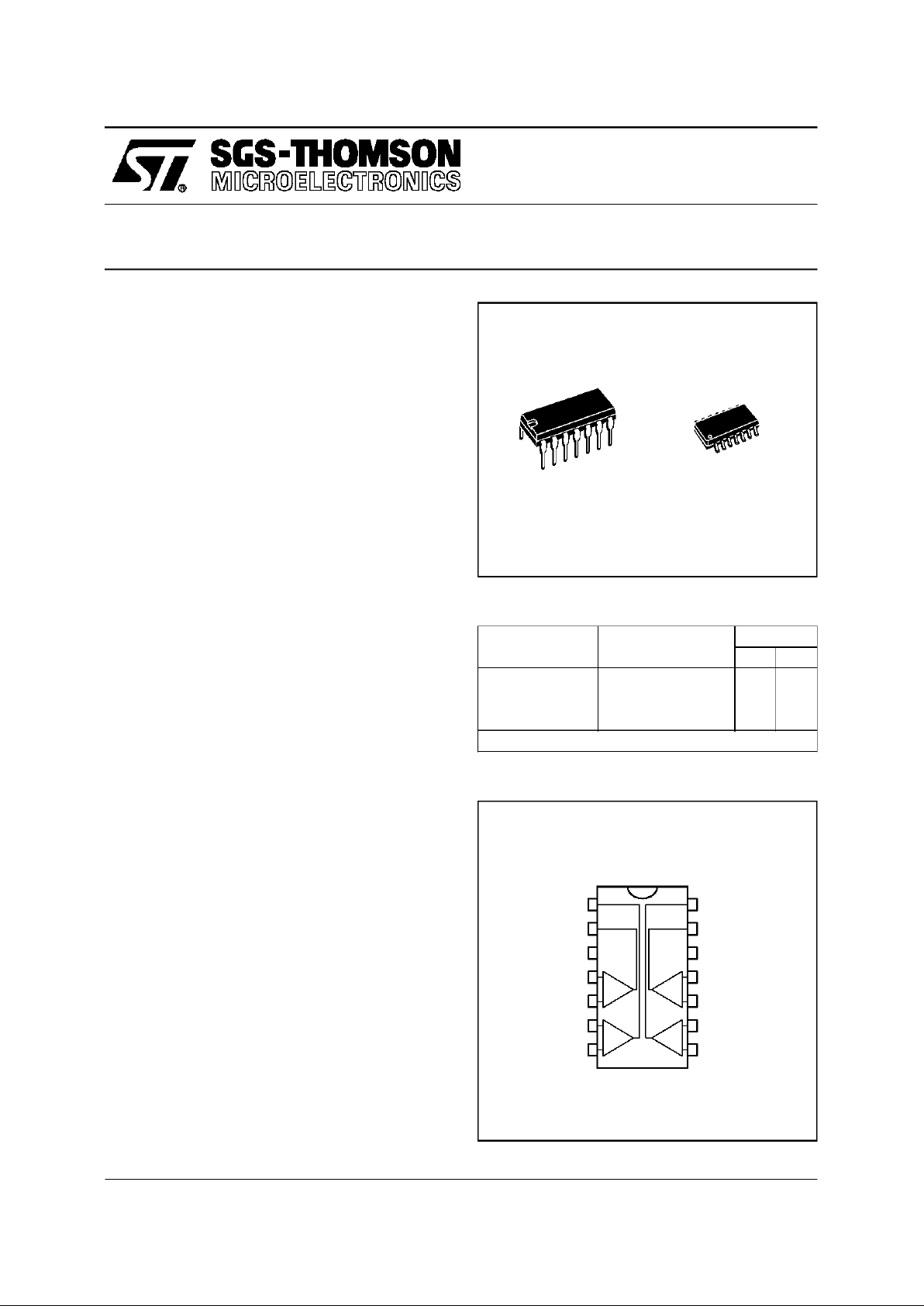
PIN CONNECTIONS (top view)
N
DIP14
(Plastic Package)
D
SO14
(Plastic Micropackage)
October 1997
ORDER CODES
Part Number
Temperature
Range
Package
ND
TS374C 0
o
C, +70oC ●●
TS374I -40oC, +125oC ●●
TS374M -55oC, +125oC ●●
Example : TS374CN
DESCRIPTION
These devices consist of four independentprecisionvoltagecomparators,designedtooperatewith
single or dual supplies.
These differential comparators use the SGSTHOMSONsilicon linMOSprocess givingtheman
excellent consumption-speedratio.
These devices are ideallysuited for lowconsumption applications.
1/5
Output
Input - Input +
T
1
T
2
R
1
TT
T
T
T
34
7
8
9
T
T
T
T
T
T
T
T
T
T
T
T
T
T
T
T
T
T
T
T
TT
T
T
TT
11
10
12
13
14
16
15
17
19
22
18
21
20
25
24
23
T
26
27
28
29
30
31
32
33 34
6
5
CC
CC
V
+
V
-
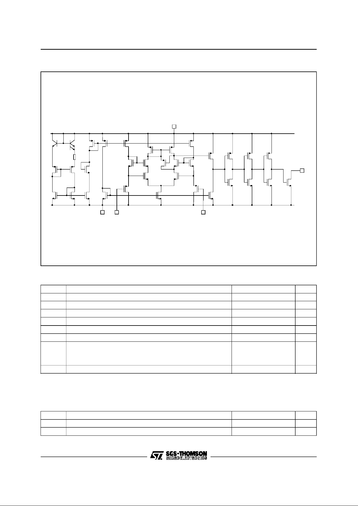
SCHEMATICDIAGRAM (for 1/4 TS374)
MAXIMUMRATINGS
Symbol Parameter Value Unit
V
CC
+
Supply Voltage - (note 1) 18 V
V
id
Differential Input Voltage - (note2) ±18 V
V
i
Input Voltage- (note 3) 18 V
V
O
Output Voltage 18 V
I
O
Output Current 20 mA
Duration of Output Short-Circuit to GND - (note 4) Infinite
T
oper
Operating Free-Air TemperatureRange
TS374C
TS374I
TS374M
0 to +70
-40 to +125
-55 to +125
o
C
T
stg
Storage TemperatureRange -65 to +150
o
C
Notes : 1. All voltage values, except differential voltage,are with respect tonetwork ground terminal.
2. Differential voltages are thenon-inverting input terminal with respect to the inverting input terminal.
3. The magnitude of theinput and the output voltages must never exceed the magnitude of thepositive supply voltage.
4. Short circuit fromoutputs to V
CC
+
can cause excessiveheating and eventualdestruction.
OPERATINGCONDITIONS
Symbol Parameter Value Unit
V
CC
+
Supply Voltage 3 to16 V
V
icm
Common Mode Input Voltage Range 0 to V
CC
+
-1.5 V
TS374C,I,M
2/5
 Loading...