

TS372C,I,M
LOW POWERDUAL CMOS VOLTAGE COMPARATORS
.
WIDE SINGLE SUPPLY RANGE OR DUAL
SUPPLIES3VTO 16V OR ±1.5V to ±8V
.
VERY LOW SUPPLY CURRENT :
0.1mA/COMP INDEPENDENT OF SUPPLY
VOLTAGE
.
EXTREMELY LOW INPUT BIAS CURRENT :
1pA TYP
.
EXTREMELY LOW INPUT OFFSET
CURRENT: 1pATYP
.
LOW INPUT OFFSETVOLTAGE
.
INPUT COMMON-MODE VOLTAGE RANGE
INCLUDESGND
.
LOW OUTPUT SATURATION VOLTAGE
150mV TYP
.
OUTPUTCOMPATIBLE WITH TTL,MOSAND
CMOS
.
HIGHINPUTIMPEDANCE1012Ω TYP
.
FAST RESPONSE TIME : 200ns TYP FOR
TTL LEVEL INPUT STEP
1
2
3
45
6
7
8
CC
+
-
-
+
-
+
CC
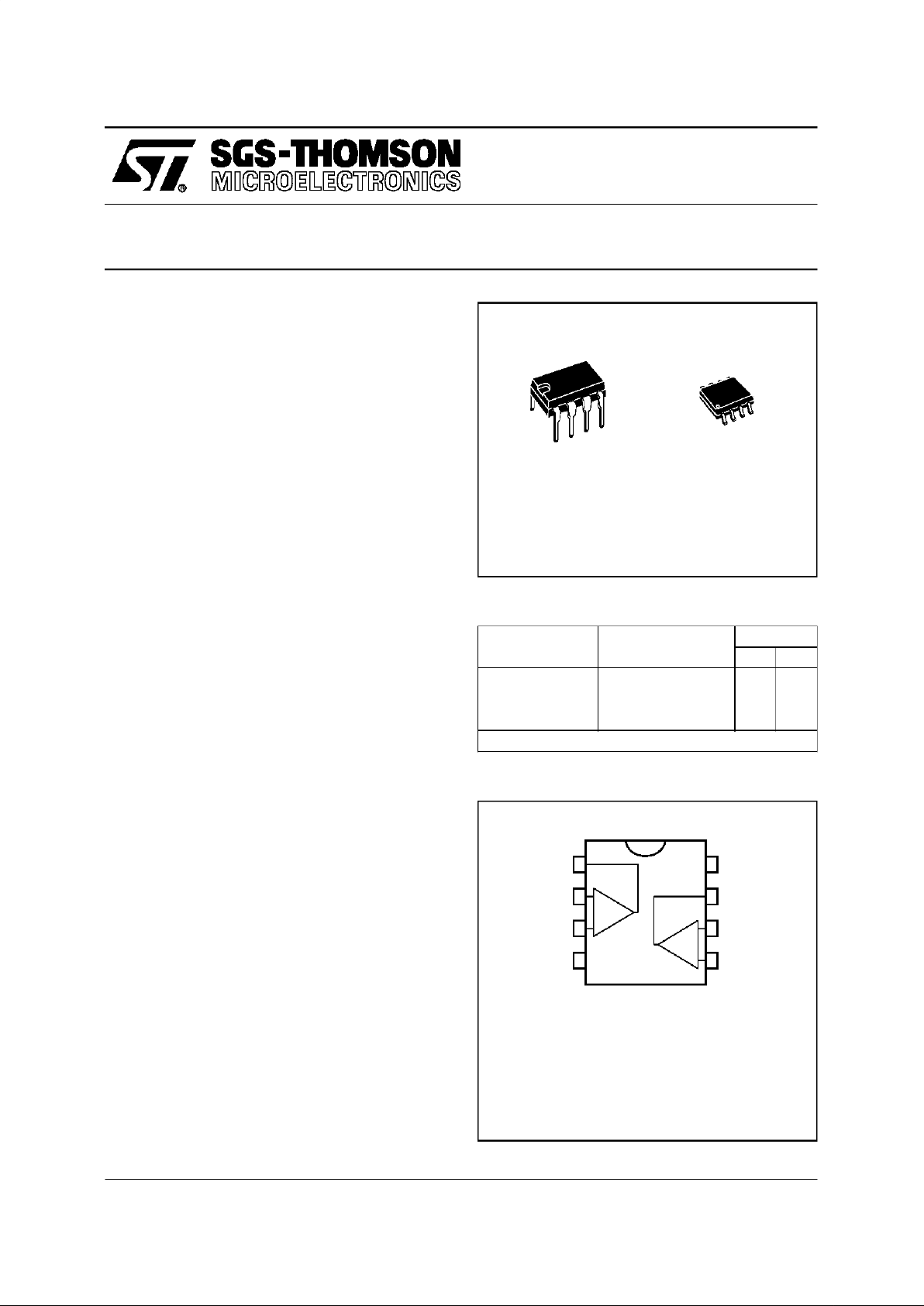
1 - Output 1
2 - Inverting Input 1
3 - Non-invertingInput 1
4-V
5 - Non-invertingInput 2
6 - Inverting Input 2
7 - Output 2
8-V
PIN CONNECTIONS (top view)
N
DIP8
(Plastic Package)
D
SO8
(Plastic Micropackage)
October 1997
ORDER CODES
Part Number
Temperature
Range
Package
ND
TS372C 0
o
C, +70oC ●●
TS372I -40oC, +125oC ●●
TS372M -55oC, +125oC ●●
Example : TS372CN
DESCRIPTION
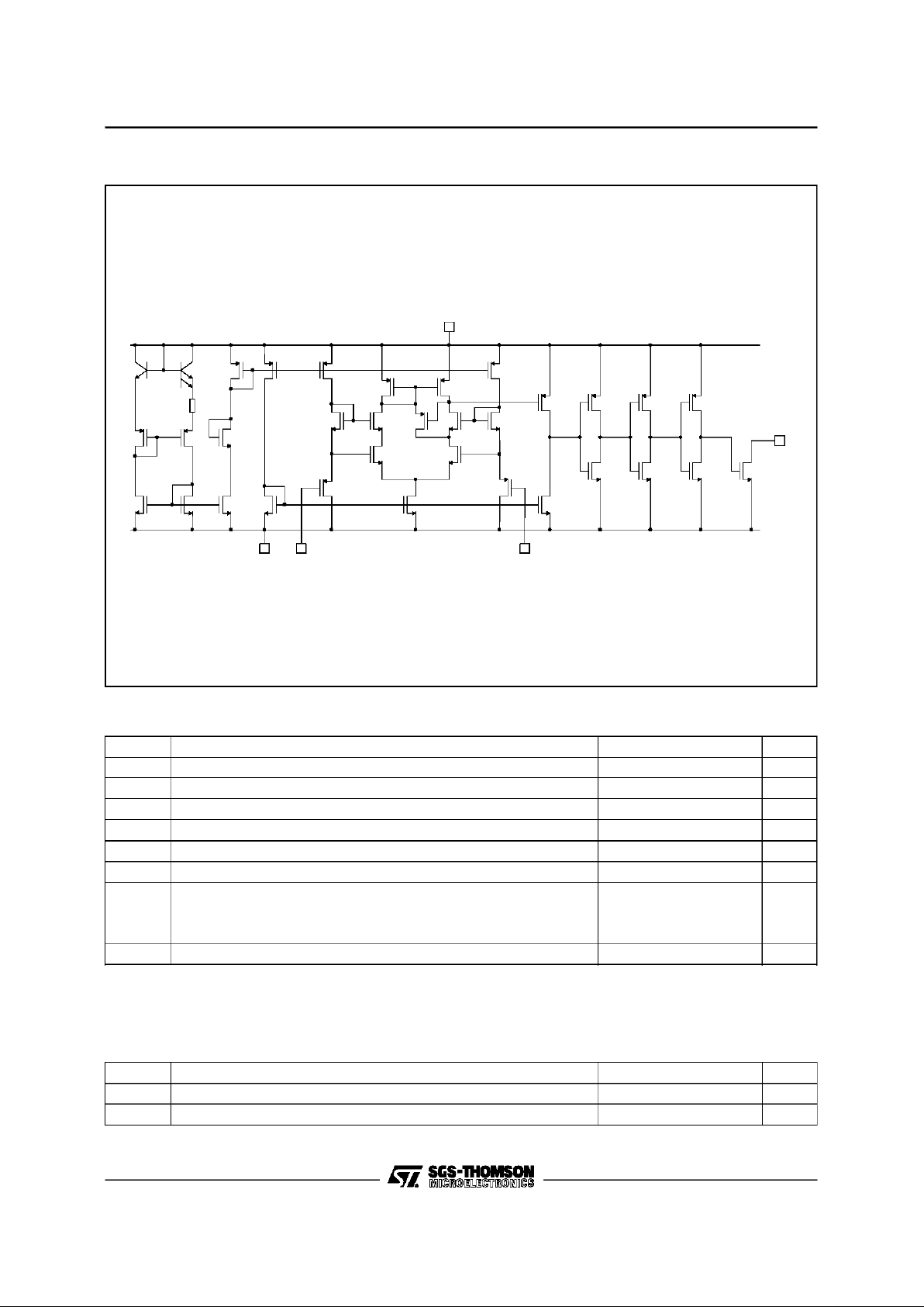
These devices consist of two independentprecisionvoltagecomparators,designedtooperatewith
single or dual supplies.
These differential comparators use the SGSTHOMSONsiliconlin MOSprocess givingtheman
excellent consumption-speedratio.
These devices are ideally suited for lowconsumption applications.
1/5
Output
Input - Input +
T
1
T
2
R
1
TT
T
T
T
34
7
8
9
T
T
T
T
T
T
T
T
T
T
T
T
T
T
T
T
T
T
T
T
TT
T
T
TT
11
10
12
13
14
16
15
17
19
22
18
21
20
25
24
23
T
26
27
28
29
30
31
32
33 34
6
5
CC
CC
V
+
V
-
SCHEMATIC DIAGRAM (for 1/2 TS372)
MAXIMUMRATINGS
Symbol Parameter Value Unit
V
CC
+
Supply Voltage - (note 1) 18 V
V
id
Differential Input Voltage - (note 2) ±18 V
V
i
Input Voltage- (note 3) 18 V
V
O
Output Voltage 18 V
I
O
Output Current 20 mA
Duration of Output Short-Circuit to GND - (note 4) Infinite
T
oper
Operating Free-Air TemperatureRange
TS372C
TS372I
TS372M
0 to +70
-40 to +125
-55 to +125
o
C
T
stg
Storage TemperatureRange -65 to +150
o
C
Notes : 1. All voltagevalues, exceptdifferential voltage,are withrespect to networkground terminal.
2. Differential voltages are the non-inverting input terminal with respect to the inverting input terminal.
3. The magnitude of the input and the output voltages must never exceed the magnitude of the positive supplyvoltage.
4. Short circuit from outputs to V
CC
+
can cause excessive heatingand eventual destruction.
OPERATINGCONDITIONS
Symbol Parameter Value Unit
V
CC
+
Supply Voltage 3 to16 V
V
icm
Common Mode Input Voltage Range 0 to V
CC
+
-1.5 V
TS372C,I,M
2/5

ELECTRICAL CHARACTERISTICS
V
CC
+
= 5V, V
CC
-
= 0V, T
amb
=25oC (unlessotherwisespecified)
Symbol Parameter Min. Typ. Max. Unit
V
io
Input Offset Voltage(Vic=V
icm min.
) - (note 1)
T
amb
=25oC
T
min.
≤ T
amb
≤T
max
.
210
12
mV
I
io
Input Offset Current- (note2)
T
amb
=25oC
T
min.
≤ T
amb
≤T
max
. TS372C
TS372I/TS372M
1
100
200
pA
I
ib
Input Bias Current - (note 2)
T
amb
=25oC
T
min.
≤ T
amb
≤T
max
. TS372C
TS372I/TS372M
1
150
300
pA
V
icm
Input Common Mode VoltageRange
T
amb
=25oC
T
min.
≤ T
amb
≤T
max
. TS372C
TS372I/TS372M
0toV
CC
+
-2
0toV
CC
+
-2.25
0toV
CC
+
-2.5
V
I
OH
High Level Output Current (Vid= 1V)
T
amb
=25oCV
OH
=5V
T
min.
≤ T
amb
≤T
max
.V
OH
= 15V
0.1
1
nA
µA
V
OL
Low Level Output Voltage (Vid= -1V,I
OL=
4mA)
T
amb
=25oC
T
min.
≤ T
amb
≤T
max
.
100 400
700
mV
I
OL
Low Level Output Current (Vid= -1V,VOL= 1.5V) 6 45 mA
I
CC
Supply Current (2 comparators) (Vid= +1V,no load) 0.3 0.75 mA
SWITCHING CHARACTERISTICS (V
CC
+
= 5V, T
amb
=25oC)
Symbol Parameter Min. Typ. Max. Unit
t
re
Response Time (RL= 5.1kΩ connected to 5V,CL= 15pF - (note 3)
• 100mV input step with 5mV overdrive
• TTL level inputstep
600
200
ns
Notes : 1. The specified offset voltageis the maximum value required to drive the output down to 400mVor up
to 4V with R
L
= 100kΩ to V
CC
+
.
2. Maximum values including unavoidable inaccuraciesof the industrial test.
3. The response time which is specified is theinternal between the input signal and the instant when the output signal crosses 1.4V.
TS372C,I,M
3/5

PMDIP8.EPS
PACKAGE MECHANICAL DATA
8 PINS- PLASTICDIP
Dimensions
Millimeters Inches
Min. Typ. Max. Min. Typ. Max.
A 3.32 0.131
a1 0.51 0.020
B 1.15 1.65 0.045 0.065
b 0.356 0.55 0.014 0.022
b1 0.204 0.304 0.008 0.012
D 10.92 0.430
E 7.95 9.75 0.313 0.384
e 2.54 0.100
e3 7.62 0.300
e4 7.62 0.300
F 6.6 0260
i 5.08 0.200
L 3.18 3.81 0.125 0.150
Z 1.52 0.060
DIP8.TBL
TS372C,I,M
4/5

Information furnished is believed tobe accurate and reliable. However, SGS-THOMSON Microelectronics assumes no responsibility
for the consequences of use of such information nor forany infringement of patents or otherrights of third parties which may result
from itsuse. No license isgranted byimplication or otherwiseunder anypatent or patent rights ofSGS-THOMSON Microelectronics.
Specification mentioned in this publication are subject to change without notice. This publication supersedes and replaces all
information previously supplied. SGS-THOMSON Microelectronics products are not authorized for use as critical components in life
support devices or systems withoutexpress written approval of SGS-THOMSON Microelectronics.
1997 SGS-THOMSON Microelectronics – Printed in Italy – AllRights Reserved
SGS-THOMSONMicroelectronics GROUP OF COMPANIES
Australia - Brazil- Canada - China - France - Germany - Hong Kong - Italy - Japan - Korea - Malaysia - Malta - Morocco
The Netherlands - Singapore - Spain - Sweden - Switzerland - Taiwan - Thailand - United Kingdom - U.S.A.
ORDER CODE :
PM-SO8.EPS
PACKAGE MECHANICAL DATA
8 PINS- PLASTICMICROPACKAGE(SO)
Dimensions
Millimeters Inches
Min. Typ. Max. Min. Typ. Max.
A 1.75 0.069
a1 0.1 0.25 0.004 0.010
a2 1.65 0.065
a3 0.65 0.85 0.026 0.033
b 0.35 0.48 0.014 0.019
b1 0.19 0.25 0.007 0.010
C 0.25 0.5 0.010 0.020
c1 45
o
(typ.)
D 4.8 5.0 0.189 0.197
E 5.8 6.2 0.228 0.244
e 1.27 0.050
e3 3.81 0.150
F 3.8 4.0 0.150 0.157
L 0.4 1.27 0.016 0.050
M 0.6 0.024
S8
o
(max.)
SO8.TBL
TS372C,I,M
5/5
 Loading...