

SGS Thomson Microelectronics TS3702IN, TS3702ID, TS3702I, TS3702CN, TS3702CD Datasheet
...
MICROPOWER DUALCMOS VOLTAGE COMPARATORS
.
PUSH-PULL CMOS OUTPUT (NO EXTERNALPULL-UPRESISTORREQUIRED)
.
EXTREMELY LOW SUPPLY CURRENT :
9µATYP / COMPARATOR
.
WIDE SINGLE SUPPLYRANGE (3V TO 16V)
ORDUAL SUPPLIES (± 1.5V TO ± 8V)
.
EXTREMELY LOW INPUT BIAS CURRENT :
1pATYP
.
EXTREMELY LOW INPUT OFFSET
CURRENT : 1pATYP
.
INPUT COMMON-MODE VOLTAGE RANGE
INCLUDESGND
.
HIGH INPUT IMPEDANCE : 1012Ω TYP
.
FASTRESPONSETIME : 2µs TYP FOR 5mV
OVERDRIVE
.
PIN-TO-PIN AND FUNCTIONALLY COMPATIBLE WITH BIPOLAR LM393
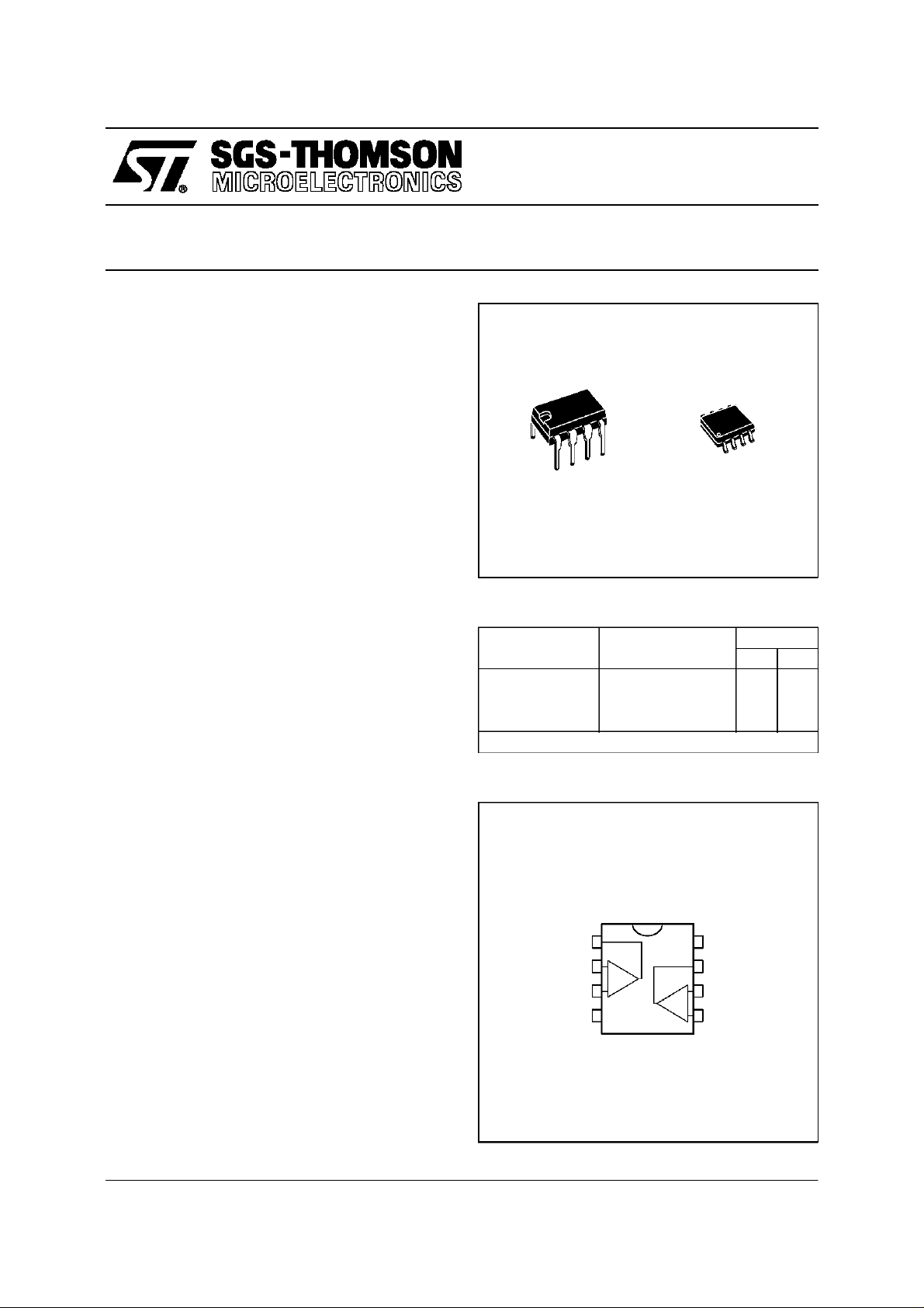
TS3702C,I,M
N
DIP8
(Plastic Package)
ORDERCODES
Part Number
TS3702C 0
TS3702I -40oC, +125oC ●●
TS3702M -55oC, +125oC ●●
Example : TS3702CN
(Plastic Micropackage)
Temperature
Range
o
C, +70oC ●●
D
SO8
Package
ND
DESCRIPTION
The TS3702 is a micropowerCMOS dual voltage
comparator with extremely low consumption of
9µA typ / comparator (20 times less than bipolar
LM393). The push-pull CMOSoutput stage allows
powerandspacesavingbyeliminatingthe external
pull-up resistor required by usual open-collector
output comparators.
Thusresponse times remain similar to the LM393.
October 1997
PIN CONNECTIONS (top view)
1
Output 1
InvertingInput 1
Non-invertingInput 1
2
-
+
3
-
V
45
CC
+
+
8
V
CC
7
Output2
6
InvertingInput 2
-
Non-invertingInput 2
1/5
TS3702C,I,M
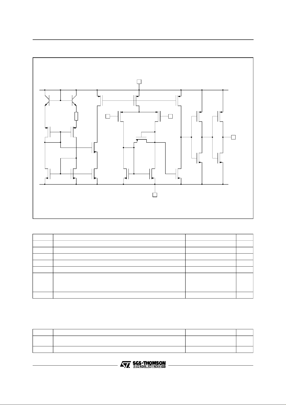
SCHEMATIC DIAGRAM (for 1/2TS3702)
T
1
T
2
T
9
V+
CC
T
10
T
17
R
1
Input- Input+
TT
34
T
8
T
5
T
6
T
7
T
11
TT
14 15
T
12
T
13
T
16
V-
CC
TT
18 21
Output
TT
19 20
MAXIMUM RATINGS
Symbol Parameter Value Unit
+
V
V
V
T
T
Notes : 1. All voltage values, except differential voltage, are with respect to network ground terminal.
Supply Voltage- (note 1) 18 V
CC
Differential Input Voltage - (note 2) ±18 V
id
Input Voltage - (note 3) 18 V
V
i
Output Voltage 18 V
O
Output Current 20 mA
I
O
Operating Free-Air Temperature Range
oper
Storage Temperature Range -65 to +150
stg
2. Differential voltages are the non-inverting input terminal with respect tothe inverting input terminal.
3. The magnitude of the input and the output voltagesmust never exceed themagnitude of the positive supply voltage.
4. Short circuit from outputs to V
+
can cause excessive heating and eventual destruction.
CC
TS3702C
TS3702I
TS3702M
0 to +70
-40 to +125
-55 to +125
o
C
o
C
OPERATING CONDITIONS
Symbol Parameter Value Unit
+
2/5
V
V
Supply Voltage TS3702C,I
CC
Common Mode Input Voltage Range 0 to V
icm
TS3702M
3to16
4to16
+
-1.5 V
CC
V
 Loading...