

SGS Thomson Microelectronics TS339IN, TS339ID, TS339I, TS339CN, TS339CD Datasheet
...
MICROPOWER QUAD CMOS VOLTAGE COMPARATORS
.
EXTREMELYLOW SUPPLYCURRENT :
9µATYP / COMPARATOR
.
WIDE SINGLE SUPPLY RANGE (3V TO 16V)
OR DUAL SUPPLIES(±1.5V TO
.
EXTREMELY LOW INPUT BIAS CURRENT :
1pA TYP
.
EXTREMELYLOW INPUTOFFSET
CURRENT: 1pATYP
.
INPUT COMMON-MODE VOLTAGE RANGE
INCLUDESGND
.
HIGHINPUT IMPEDANCE: 1012Ω TYP
.
FASTRESPONSETIME : 1.5µs TYP FOR
5mV OVERDRIVE
.
PIN-TO-PINAND FUNCTIONALLY
COMPATIBLEWITH BIPOLAR LM339
±8V)
TS339C,I,M
N
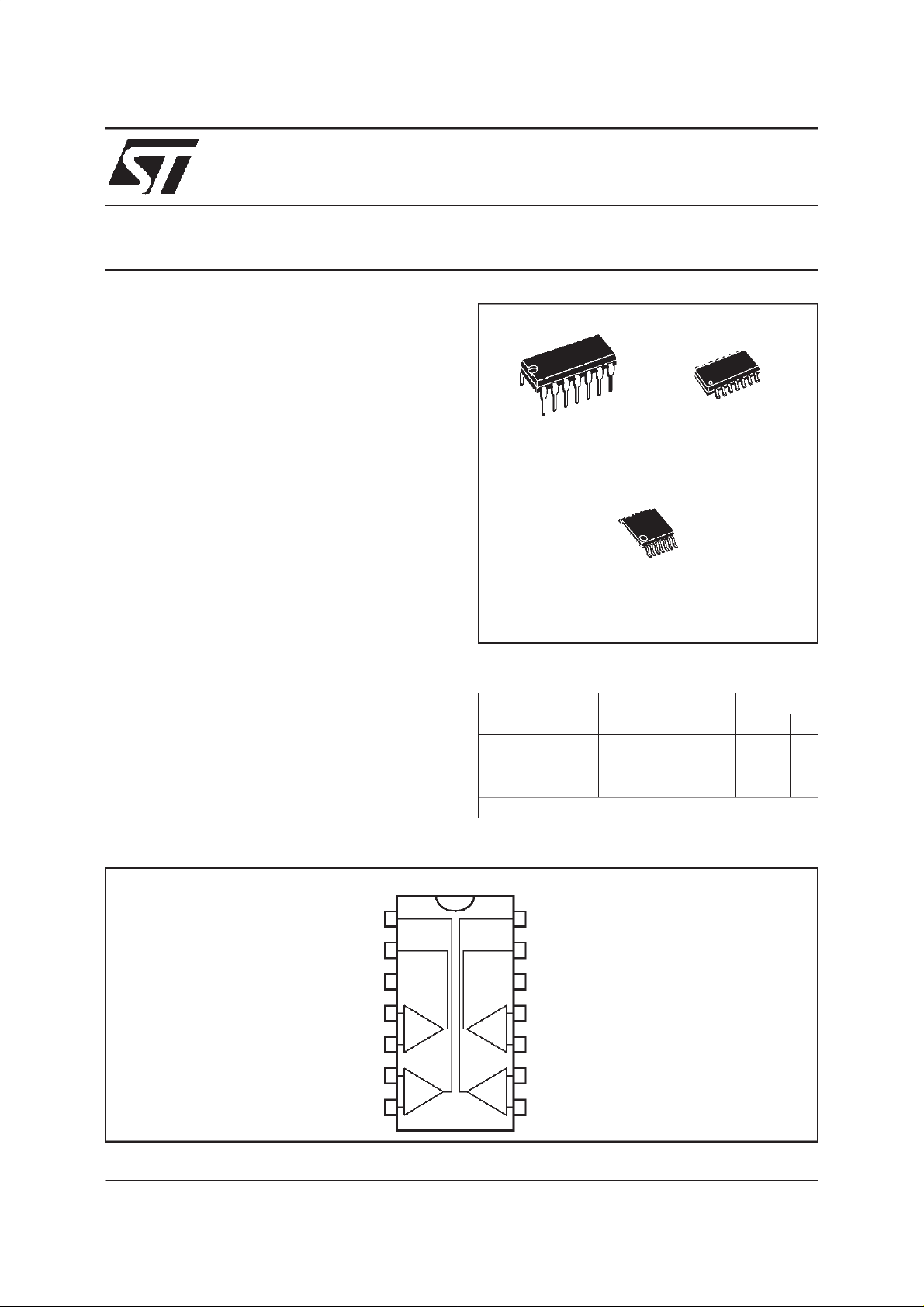
DIP14
(Plastic Package)
(Thin Shrink Small Outline Package)
(Plastic Micropackage)
P
TSSOP14
D
SO14
DESCRIPTION
The TS339 is a micropowerCMOS quad voltage
comparatorwith extremely low consumption of
9µA typ / comparator(20 times less than bipolar
LM339). Similar performancesare offered by the
quad micropowercomparatorTS3704withapushpull CMOS output.
Thus responsetimes remain similarto the LM339.
PIN CONNECTIONS (top view)
Output 2
Output 1
Inverting Input1
Non-inverting Input1
Inverting Input 2
Non-inverting Input 2
1
2
V
3
CC
4
-
+-
5
6
-
+-
7
ORDER CODES
Package
NDP
-
Temperature
Range
o
C, +70oC ●●●
Part Number
TS339C 0
TS339I -40oC, +125oC ●●●
TS339M -55oC, +125oC ●●●
Example : TS339CN
14+Output 3
13
Output 4
V
12
CC
11
+
+
Non-inverting Input 4
10
Inverting Input 4
9
Non-inverting Input 3
8
Inverting Input 3
September 1998
1/6
TS339C,I,M
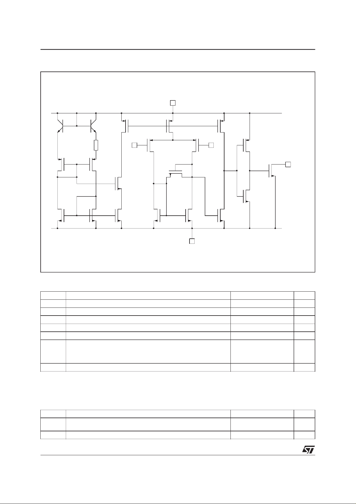
SCHEMATIC DIAGRAM (for 1/4 TS339)
T
1
T
2
T
9
V+
CC
T
10
T
17
R
1
Input - Input +
TT
34
T
8
T
5
T
6
T
7
T
11
TT
14 15
T
12
T
13
T
16
V-
CC
T
18
Output
T
20
T
19
MAXIMUMRATINGS
Symbol Parameter Value Unit
+
V
V
V
T
T
Notes : 1. Allvoltage values,except differential voltage, are with respect tonetwork ground terminal.
Supply Voltage- (note 1) 18 V
CC
Differential Input Voltage - (note2) ±18 V
id
Input Voltage- (note 3) 18 V
V
i
Output Voltage 18 V
O
Output Current 20 mA
I
O
Operating Free-Air TemperatureRange
oper
Storage TemperatureRange -65 to +150
stg
2. Differentialvoltages are the non-inverting input terminal withrespect to the inverting input terminal.
3. The magnitude of the input and the outputvoltages must never exceed the magnitude ofthe positive supplyvoltage.
4. Short circuit from outputs toV
+
can cause excessive heating andeventual destruction.
CC
TS339C
TS339I
TS339M
0 to +70
-40 to +125
-55 to +125
o
C
o
C
OPERATINGCONDITIONS
Symbol Parameter Value Unit
+
2/6
V
V
Supply Voltage TS339C,I
CC
Common Mode Input VoltageRange 0 to V
icm
TS339M
3to16
4to16
+
-1.5 V
CC
V
 Loading...