

Datasheet TS27M2M, TS27M2ACD, TS27M2ACN, TS27M2IN, TS27M2I Datasheet (SGS Thomson Microelectronics)
...Page 1
.
VERYLOWCONSUMPTIION : 150µA/op
.
OUTPUT VOLTAGE CAN SWING TO
GROUND
.
EXCELLENTPHASEMARGIN ON
CAPACITIVE LOADS
.
STABLE AND LOW OFFSETVOLTAGE
.
THREEINPUTOFFSETVOLTAGE
SELECTIONS
TS27M2C,I,M
LOW POWER CMOS
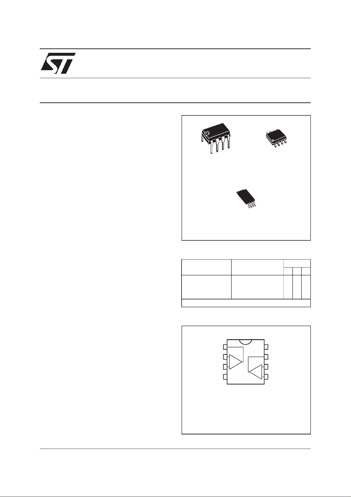
DUALOPERATIONAL AMPLIFIERS
N
DIP8
(Plastic Package)
(Thin Shrink Small Outline Package)
(Plastic Micropackage)
P
TSSOP8
D
SO8
DESCRIPTION
The TS272 series are low cost, low power dual
operational amplifiers designed to operate with
single or dual supplies.These operationalamplifiers use the SGS-THOMSON silicon gate CMOS
processallowing an excellentconsumption-speed
ratio. These series are ideallysuited for low consumption applications.
Three power consumptionsare available allowing
to havealways the bestconsumption-speedratio:
● I
=10µA/amp.: TS27L2 (very lowpower)
CC
● I
= 150µA/amp.: TS27M2 (low power)
CC
● I
= 1mA/amp.: TS272 (high speed)
CC
These CMOS amplifiers offer very high input impedance and extremely low input currents. The
major advantage versus JFET devices is the very
low input currents driftwith temperature
(see figure2).
ORDER CODES
Part Number
TS27M2C/AC/BC 0
TS27M2I/AI/BI -40oC, +125oC ●●●
TS27M2M/AM/BM -55oC, +125oC ●●●
Example : TS27M2ACN
PIN CONNECTIONS (top view)
1
2
3
45
Temperature
Range
o
C, +70oC ●●●
-
+
1 - Output 1
2 - InvertingInput1
3 - Non-invertingInput 1
-
4-V
CC
5 - Non-invertingInput 2
6 - InvertingInput2
7 - Output 2
+
8-V
CC
-
+
Package
NDP
8
7
6
June 1998
1/9
Page 2
TS27M2C,I,M
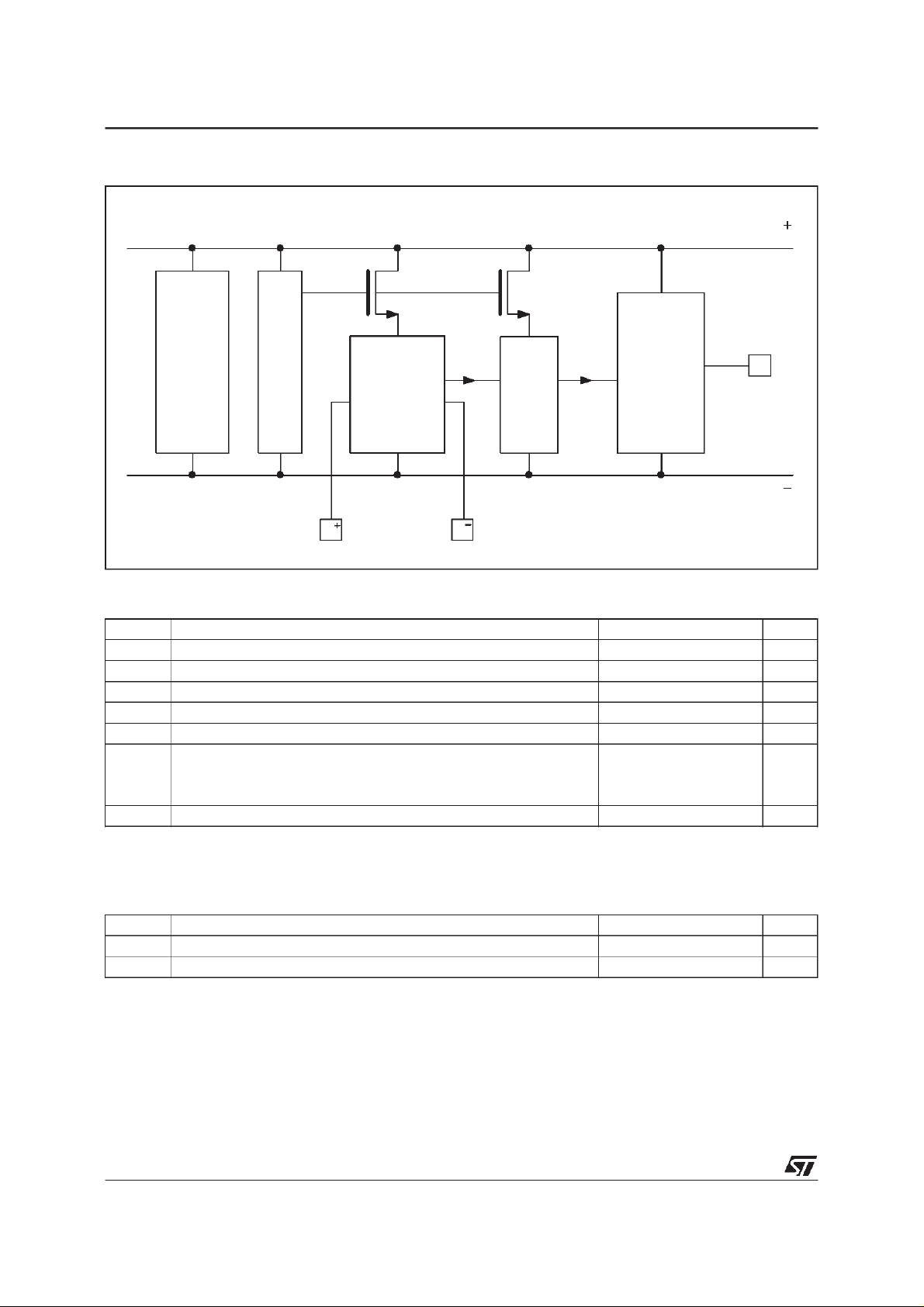
BLOCK DIAGRAM
V
CC
Current
source
xI
Input
differential
Second
stage
E E
MAXIMUMRATINGS
Symbol Parameter Value Unit
+
V
V
T
T
Notes : 1. All voltage values, except differential voltage, are withrespect to network ground terminal.
Supply Voltage - (note 1) 18 V
CC
Differential Input Voltage - (note 2) ±18 V
id
Input Voltage - (note 3) -0.3 to 18 V
V
i
Output Current for V
I
O
Input Current ±5mA
I
in
Operating Free-Air Temperature Range
oper
Storage Temperature Range -65 to +150
stg
2. Differentialvoltages are at the non-invertinginput terminal with respect to the inverting input terminal.
3. Themagnitude of the input and the output voltages must never exceed the magnitude of the positive supply voltage.
+
≥ 15V ±30 mA
CC
TS27M2C/AC/BC
TS27M2I/AI/BI
TS27M2M/AM/BM
Output
stage
0 to +70
-40 to +125
-55 to +125
Output
V
CC
o
C
o
C
OPERATING CONDITIONS
Symbol Parameter Value Unit
+
V
V
2/9
Supply Voltage 3 to 16 V
CC
Common Mode Input VoltageRange 0 to V
icm
CC
+
- 1.5 V
Page 3
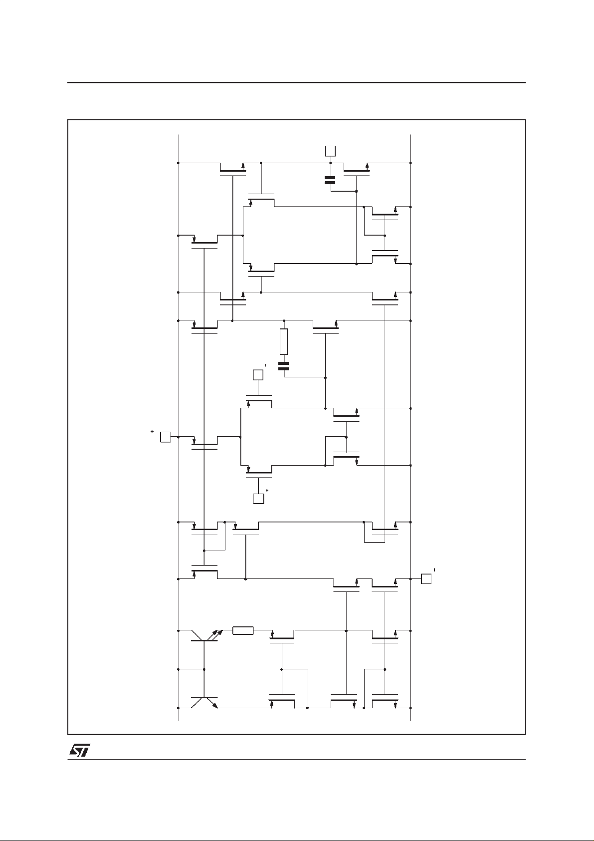
SCHEMATIC DIAGRAM (for 1/2 TS27M2)
TS27M2C,I,M
15
T
12
T
10
T
11
T
8
T
6
T
Output
7
T
16
T
14
T
13
T
9
T
R1
C1
Input
2
T
5
CC
V
T
1
T
4
T
3
T
27
T
26
T
25
T
24
T
Input
28
T
23
T
2
R
T
17 18
T
19
T
29
T
22
T
21
T
20
T
CC
V
3/9
Page 4

TS27M2C,I,M
ELECTRICAL CHARACTERISTICS
+
= +10V,V
V
CC
Symbol Parameter
V
DV
V
V
A
Input Offset Voltage
io
Input Offset Voltage Drift 2 2 µV/oC
io
Input Offset Current - (note 1)
I
io
Input Bias Current - (note 1)
I
ib
High Level Output Voltage
OH
Low Level Output Voltage
OL
Large Signal Voltage Gain
vd
GBP Gain Bandwidth Product
CMR Common Mode Rejection Ratio
SVR Supply Voltage Rejection Ratio
I
I
sink
Supply Current (per amplifier)
CC
Output Short Circuit Current
I
o
Output Sink Current
SR Slew-Rateat Unity Gain
∅m Phase Margin at Unity Gain
K
e
V
O1/VO2
Note : 1. Maximum values including unavoidable inaccuracies of the industrial test.
Overshoot Factor 30 30 %
ov
Equivalent Input Noise Voltage
n
Channel Separation 120 120 dB
-
CC
=0V,T
=25oC (unlessotherwisespecified)
amb
TS27M2C/AC/BC
Min. Typ. Max. Min. Typ. Max.
= 1.4V, Vic= 0V TS27M2C/I/M
V
O
TS27M2AC/AI/AM
TS27M2BC/BI/BM
. ≤ T
T
min
amb≤Tmax.
TS27M2C/I/M
TS27M2AC/AI/AM
1.1
0.9
0.25
TS27M2BC/BI/BM
= 5V, Vo=5V
V
ic
. ≤ T
T
min
amb≤Tmax.
= 5V, Vo=5V
V
ic
. ≤ T
T
min
amb≤Tmax.
= 100mV, RL= 100kΩ
V
id
. ≤ T
T
min
amb≤Tmax.
= -100mV 50 50
V
id
= 1V to 6V, RL= 100kΩ,Vic=5V
V
o
. ≤ T
T
min
amb≤Tmax.
8.7
8.6
30
20
8.9 8.7
50 30
Av= 40dB, RL= 100kΩ,CL= 100pF
= 100kHz
f
in
V
= 1.4V, Vic= 1V to 7.4V 65 80 65 80
o
+
V
= 5V to 10V ,Vo= 1.4V 60 80 60 80
CC
= 1, no load, Vo=5V
A
v
. ≤ T
T
min
amb≤Tmax.
= 100mV, Vo=0V 60 60
V
id
= -100mV, Vo=V
V
id
R
= 100kΩ,CL= 100pF, Vi= 3 to 7V 0.6 0.6
L
A
= 40dB, RL= 100kΩ,CL= 100pF 45 45
v
f = 1kHz, R
= 100Ω 38 38
S
CC
150 200
45 45
TS27M2I/AI/BI
TS27M2M/AM/BM
Unit
mV
10
5
2
12
6.5
3
1.1
0.9
0.25
10
5
2
12
6.5
3.5
pA
1
100
1
200
pA
1
150
1
300
V
8.9
8.5
mV
V/mV
50
10
MHz
11
dB
dB
µA
150 200
250
300
mA
mA
V/µs
Degrees
nV
√Hz
4/9
Page 5

TYPICALCHARACTERISTICS
TS27M2C,I,M
Figure 1 : SupplyCurrent (each amplifier)
versusSupply Voltage
200
T = 25 C
AMB
°
µ
CC
150
V
A=1
V=V /2
OCC
100
50
SUPPLY CURRENT, I ( A)
0481216
SUPPLY VOLTAGE, V (V)
CC
Figure 3a : High Level OutputVoltage versus
HighLevel Output Current
5
T = 25 C
AMB
°
ID
V=5V
CC
OH
4
3
V = 100mV
Figure2 : InputBias Current versus Free Air
Temperature
100
V = 10V
CC
V=5V
IB
i
10
INPUT BIAS CURRENT, I (pA)
1
25 50 75 100 125
TEMPERATURE, T ( C)
AMB
°
Figure3b : High Level OutputVoltage versus
High Level Output Current
20
T = 25 C
AMB
°
ID
V = 16V
CC
16
OH
12
V =100mV
2
V=3V
1
OUTPUT VOLTAGE, V (V)
0
-10 -8 -6 -4 -2 0
CC
OHOUTPUT CURRE NT, I (mA)
Figure 3a : Low Level OutputVoltage versus
Low Level Output Current
1.0
0.8
OL
0.6
0.4
0.2
OUTPUT VOLTAGE, V (V)
0123
V=3V
CC
V=5V
CC
T = 25 C
AMB
V = 0.5V
i
V = -1V
ID
OUTPUT CURRENT,I (mA)
OL
°
8
V = 10V
CC
4
OUTPUT VOLTAGE, V (V)
0
-50 -40 -30 -20 -10 0
OUTPUT CURRENT, I (mA)
OH
Figure3b : Low Level OutputVoltage versus
Low Level Output Current
3
OL
2
1
OUTPUT VOLTAGE, V (V)
048121620
V = 10V
CC
V = 16V
CC
T = 25 C
AMB
i
V = 0.5V
ID
V = -1V
OUTPUT CURRENT, I (mA)
OL
°
5/9
Page 6

TS27M2C,I,M
TYPICALCHARACTERISTICS (continued)
Figure 5 : Open LoopFrequencyResponse and
PhaseShift
50
40
30
20
T=25°C
10
0
V = 10V
R = 100k Ω
C = 100pF
GAIN(dB)
A = 100
-10
23
10
amb
CC
L
L
VCL
PHASE
+
10
10
4
GAIN
Gain
Bandwidth
Product
5
10
Phase
Margin
10
0
45
90
135
180
7
6
10
FREQUENCY,f (Hz)
Figure 7 : PhaseMargin versus SupplyVoltage
50
40
φ
T=25°C
30
20
PHASEMARGIN, m (Degrees)
amb
R = 100kΩ
L
C = 100pF
L
A=1
V
04 8 1216
SUPPLY VOLTAGE, V (V)
CC
Figure6 : GainBandwidth Productversus
Supply Voltage
1800
T=25°C
amb
R = 100kΩ
1400
L
C =100pF
L
A=1
V
1000
PHASE(Degrees)
600
200
GAIN BANDW.PROD.,GBP(kHz)
04 81216
SUPPLYVOLTAGE, V (V)
CC
Figure8 : PhaseMarginversus Capacitive Load
80
T=25°C
amb
R = 100kΩ
70
φ
60
50
40
PHASEMARGIN, m (Degrees)
0 20 40 60 80 100
CAPACITANCE, C (pF)
L
A=1
V
V = 10V
CC
L
Figure 9 : Slew Rate versusSupply Voltage
0.9
T=25°C
6/9
amb
R = 100kΩ
0.8
L
C = 100pF
L
0.7
0.6
0.5
SLEW RATES,SR (V/µs)
0.4
46 810121416
SUPPLY VOLTAGE, V (V)
SR
SR
CC
Figure10 : Input VoltageNoise versus Frequency
300
=10V
V
CC
T
=25°C
amb
=100Ω
R
200
100
VOLTAGE(nV/VHz)
EQUIVALENTINPUTNOISE
0
1 10
FREQUENCY(Hz)
S
100 1000
Page 7

PACKAGE MECHANICAL DATA
8 PINS - PLASTIC DIP
TS27M2C,I,M
Dimensions
Min. Typ. Max. Min. Typ. Max.
Millimeters Inches
A 3.32 0.131
a1 0.51 0.020
B 1.15 1.65 0.045 0.065
b 0.356 0.55 0.014 0.022
b1 0.204 0.304 0.008 0.012
D 10.92 0.430
E 7.95 9.75 0.313 0.384
e 2.54 0.100
e3 7.62 0.300
e4 7.62 0.300
F 6.6 0260
i 5.08 0.200
L 3.18 3.81 0.125 0.150
Z 1.52 0.060
PM-DIP8.EPS
DIP8.TBL
7/9
Page 8

TS27M2C,I,M
PACKAGE MECHANICAL DATA
8 PINS - PLASTIC MICROPACKAGE(SO)
Dimensions
Min. Typ. Max. Min. Typ. Max.
Millimeters Inches
A 1.75 0.069
a1 0.1 0.25 0.004 0.010
a2 1.65 0.065
a3 0.65 0.85 0.026 0.033
b 0.35 0.48 0.014 0.019
b1 0.19 0.25 0.007 0.010
C 0.25 0.5 0.010 0.020
c1 45
o
(typ.)
D 4.8 5.0 0.189 0.197
E 5.8 6.2 0.228 0.244
e 1.27 0.050
e3 3.81 0.150
F 3.8 4.0 0.150 0.157
L 0.4 1.27 0.016 0.050
M 0.6 0.024
S8
o
(max.)
PM-SO8.EPS
SO8.TBL
8/9
Page 9

PACKAGE MECHANICAL DATA
8 PINS- THIN SHRINK SMALL OUTLINEPACKAGE
TS27M2C,I,M
Dim.
Min. Typ. Max. Min. Typ. Max.
Millimeters Inches
A 1.20 0.05
A1 0.05 0.15 0.01 0.006
A2 0.80 1.00 1.05 0.031 0.039 0.041
b 0.19 0.30 0.007 0.15
c 0.09 0.20 0.003 0.012
D 2.90 3.00 3.10 0.114 0.118 0.122
E 6.40 0.252
E1 4.30 4.40 4.50 0.169 0.173 0.177
e 0.65 0.025
k0
o
o
8
o
0
o
8
l 0.50 0.60 0.75 0.09 0.0236 0.030
Information furnished is believed to be accurate and reliable. However, STMicroelectronics assumes no responsibility for the
consequences of use of such information nor for any infringement of patents or other rights of third parties which may result from
its use. No license is grantedby implication or otherwise under any patent or patent rights of STMicroelectronics. Specifications
mentioned in this publication are subject to change without notice. This publication supersedes and replaces all information
previously supplied.STMicroelectronics products are not authorizedfor useas criticalcomponentsinlifesupportdevices or systems
without express written approvalof STMicroelectronics.
The ST logo is a trademark of STMicroelectronics
1998 STMicroelectronics – Printed in Italy – AllRightsReserved
STMicroelectronics GROUP OF COMPANIES
Australia- Brazil - Canada - China- France- Germany - Italy - Japan - Korea -Malaysia - Malta - Mexico - Morocco
The Netherlands - Singapore - Spain - Sweden - Switzerland - Taiwan- Thailand - United Kingdom - U.S.A.
ORDERCODE :
9/9
 Loading...