

SGS Thomson Microelectronics TS27M2M, TS27M2ACD, TS27M2ACN, TS27M2IN, TS27M2I Datasheet
...
.
VERYLOWCONSUMPTIION : 150µA/op
.
OUTPUT VOLTAGE CAN SWING TO
GROUND
.
EXCELLENTPHASEMARGIN ON
CAPACITIVE LOADS
.
STABLE AND LOW OFFSETVOLTAGE
.
THREEINPUTOFFSETVOLTAGE
SELECTIONS
TS27M2C,I,M
LOW POWER CMOS
DUALOPERATIONAL AMPLIFIERS
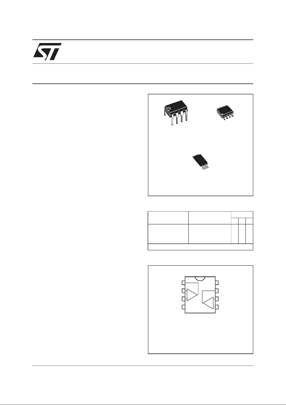
N
DIP8
(Plastic Package)
(Thin Shrink Small Outline Package)
(Plastic Micropackage)
P
TSSOP8
D
SO8
DESCRIPTION
The TS272 series are low cost, low power dual
operational amplifiers designed to operate with
single or dual supplies.These operationalamplifiers use the SGS-THOMSON silicon gate CMOS
processallowing an excellentconsumption-speed
ratio. These series are ideallysuited for low consumption applications.
Three power consumptionsare available allowing
to havealways the bestconsumption-speedratio:
● I
=10µA/amp.: TS27L2 (very lowpower)
CC
● I
= 150µA/amp.: TS27M2 (low power)
CC
● I
= 1mA/amp.: TS272 (high speed)
CC
These CMOS amplifiers offer very high input impedance and extremely low input currents. The
major advantage versus JFET devices is the very
low input currents driftwith temperature
(see figure2).
ORDER CODES
Part Number
TS27M2C/AC/BC 0
TS27M2I/AI/BI -40oC, +125oC ●●●
TS27M2M/AM/BM -55oC, +125oC ●●●
Example : TS27M2ACN
PIN CONNECTIONS (top view)
1
2
3
45
Temperature
Range
o
C, +70oC ●●●
-
+
1 - Output 1
2 - InvertingInput1
3 - Non-invertingInput 1
-
4-V
CC
5 - Non-invertingInput 2
6 - InvertingInput2
7 - Output 2
+
8-V
CC
-
+
Package
NDP
8
7
6
June 1998
1/9
TS27M2C,I,M
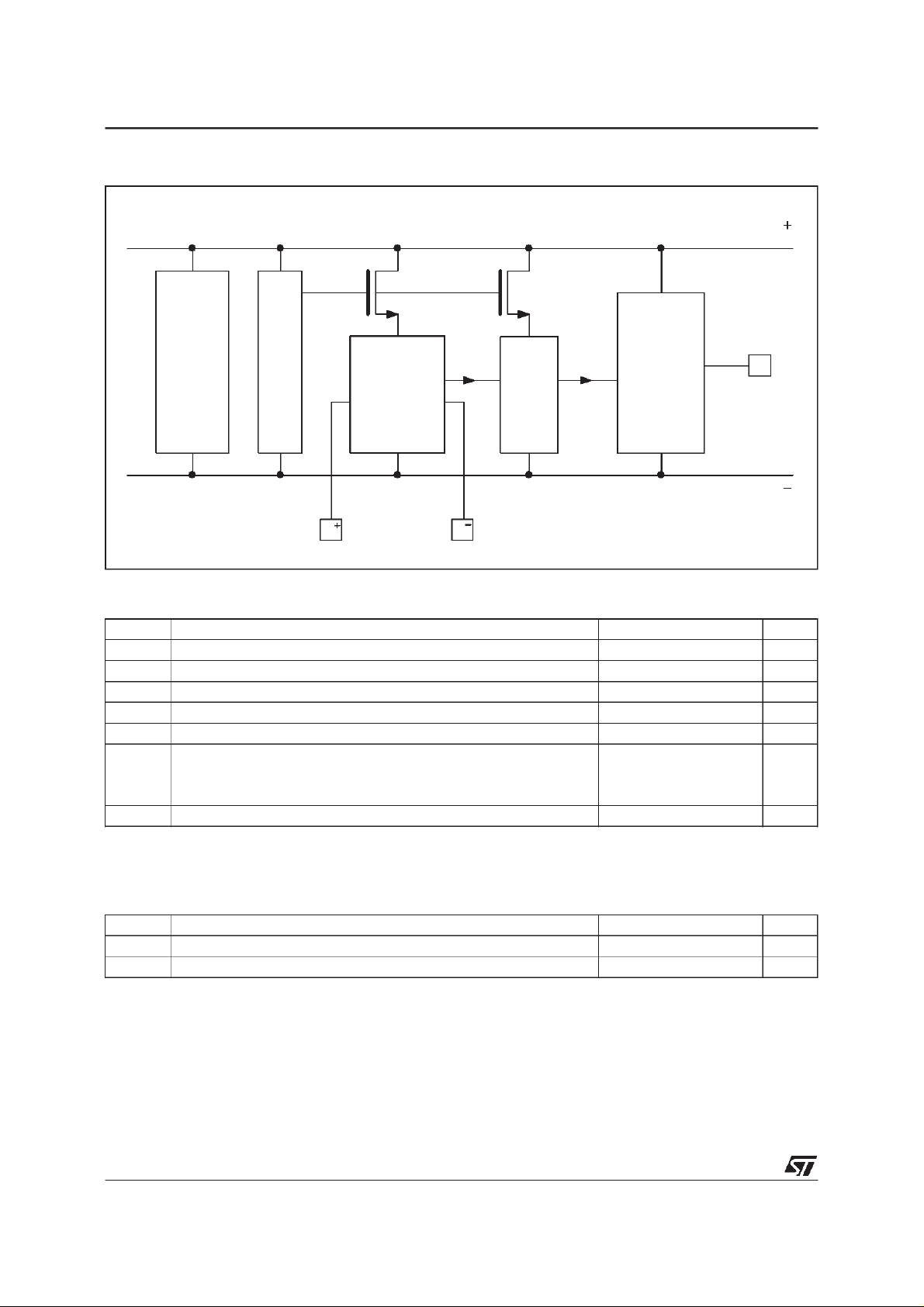
BLOCK DIAGRAM
V
CC
Current
source
xI
Input
differential
Second
stage
E E
MAXIMUMRATINGS
Symbol Parameter Value Unit
+
V
V
T
T
Notes : 1. All voltage values, except differential voltage, are withrespect to network ground terminal.
Supply Voltage - (note 1) 18 V
CC
Differential Input Voltage - (note 2) ±18 V
id
Input Voltage - (note 3) -0.3 to 18 V
V
i
Output Current for V
I
O
Input Current ±5mA
I
in
Operating Free-Air Temperature Range
oper
Storage Temperature Range -65 to +150
stg
2. Differentialvoltages are at the non-invertinginput terminal with respect to the inverting input terminal.
3. Themagnitude of the input and the output voltages must never exceed the magnitude of the positive supply voltage.
+
≥ 15V ±30 mA
CC
TS27M2C/AC/BC
TS27M2I/AI/BI
TS27M2M/AM/BM
Output
stage
0 to +70
-40 to +125
-55 to +125
Output
V
CC
o
C
o
C
OPERATING CONDITIONS
Symbol Parameter Value Unit
+
V
V
2/9
Supply Voltage 3 to 16 V
CC
Common Mode Input VoltageRange 0 to V
icm
CC
+
- 1.5 V
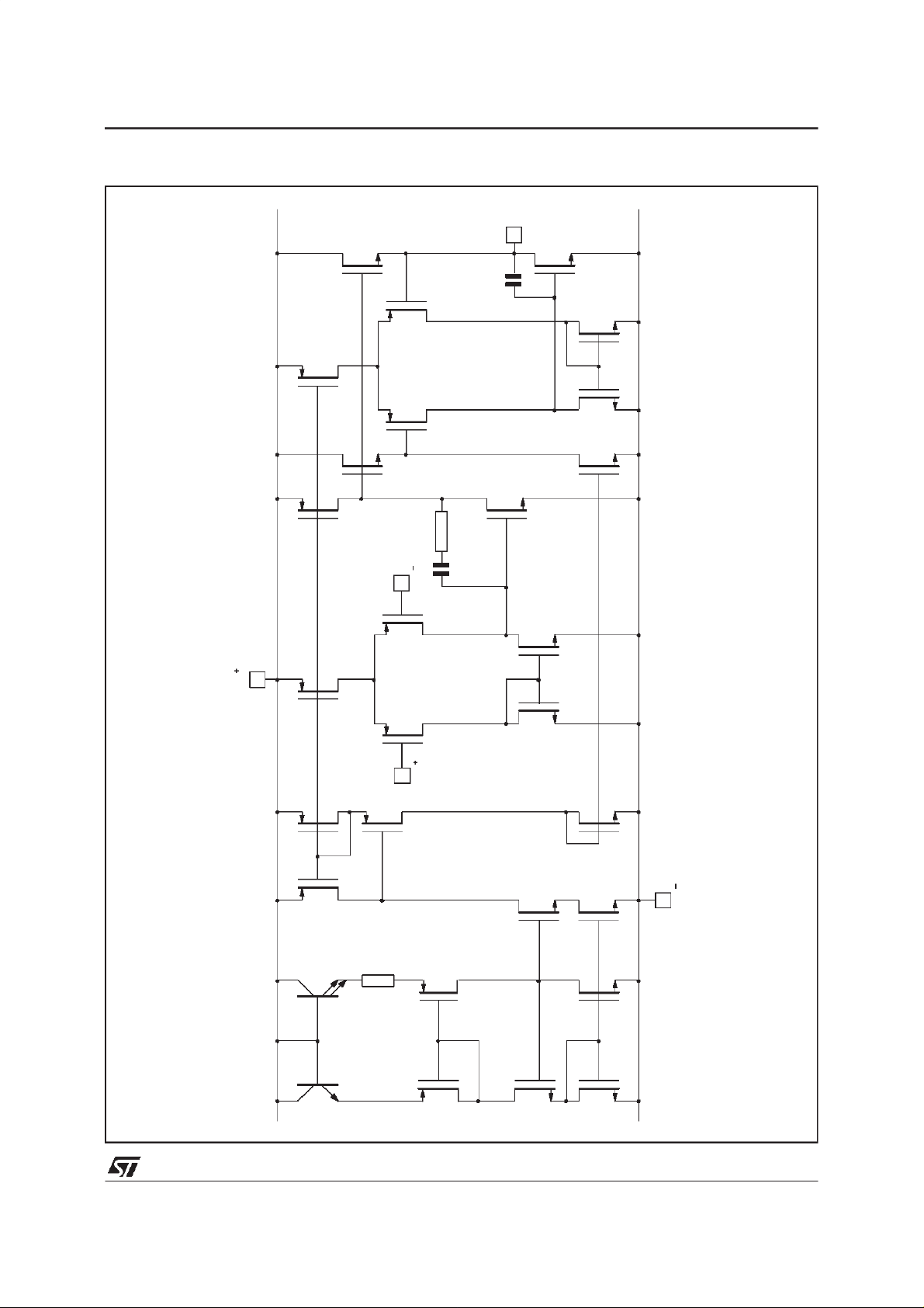
SCHEMATIC DIAGRAM (for 1/2 TS27M2)
TS27M2C,I,M
15
T
12
T
10
T
11
T
8
T
6
T
Output
7
T
16
T
14
T
13
T
9
T
R1
C1
Input
2
T
5
CC
V
T
1
T
4
T
3
T
27
T
26
T
25
T
24
T
Input
28
T
23
T
2
R
T
17 18
T
19
T
29
T
22
T
21
T
20
T
CC
V
3/9
 Loading...