

Datasheet TS27L4M, TS27L4IN, TS27L4ID, TS27L4I, TS27L4AIN Datasheet (SGS Thomson Microelectronics)
...
TS27L4C,I,M
VERYLOW POWER CMOS
QUAD OPERATIONAL AMPLIFIERS
November 1998
.
ULTRA LOWCONSUMPTIION : 10µA/op
.
OUTPUT VOLTAGE CAN SWING TO
GROUND
.
EXCELLENTPHASE MARGIN ON
CAPACITIVE LOADS
.
STABLE AND LOW OFFSETVOLTAGE
.
THREEINPUTOFFSETVOLTAGE
SELECTIONS
Inverting Input 2
Non-inverting Input 2
Non-inverting Input 1
CC
V
-
CC
V
1
2
3
4
8
5
6
7
9
10
11
12
13
14
+
Output 3
Output 4
Non-inverting Input 4
Inverting Input 4
Non-inverting Input 3
Inverting Input 3
-
+
-
+
-
+
-
+
Output 1
Inverting Input 1
Output 2
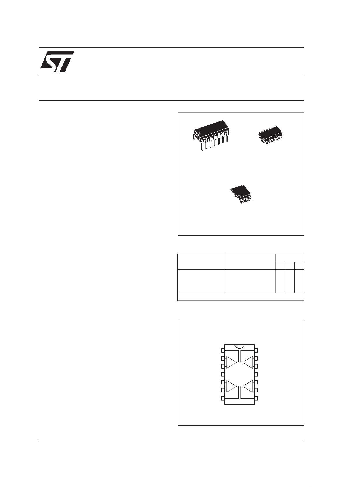
PIN CONNECTIONS (top view)
N
DIP14
(Plastic Package)
D
SO14
(Plastic Micropackage)
DESCRIPTION
The TS274 series are low cost, low power quad
operational amplifiers designed to operate with
single or dual supplies. These operationalamplifiers use the SGS-THOMSON silicon gate CMOS
process allowing an excellentconsumption-speed
ratio. These series are ideally suited for low consumption applications.
Three power consumptions are availableallowing
to have always the best consumption-speed ratio:
● I
CC
=10µA/amp.: TS27L4 (very lowpower)
● I
CC
= 150µA/amp. : TS27M4 (low power)
● I
CC
= 1mA/amp. : TS274 (high speed)
These CMOS amplifiers offer very high input impedance and extremely low input currents. The
major advantageversus JFET devices is the very
low inputcurrents driftwith temperature
(see figure2).
ORDER CODES
Part Number
Temperature
Range
Package
NDP
TS27L4C/AC/BC 0
o
C, +70oC ●●●
TS27L4I/AI/BI -40oC, +125oC ●●●
TS27L4M/AM/BM -55oC, +125oC ●●●
Example :TS27M4ACN
P
TSSOP14
(Thin Shrink Small Outline Package)
1/9
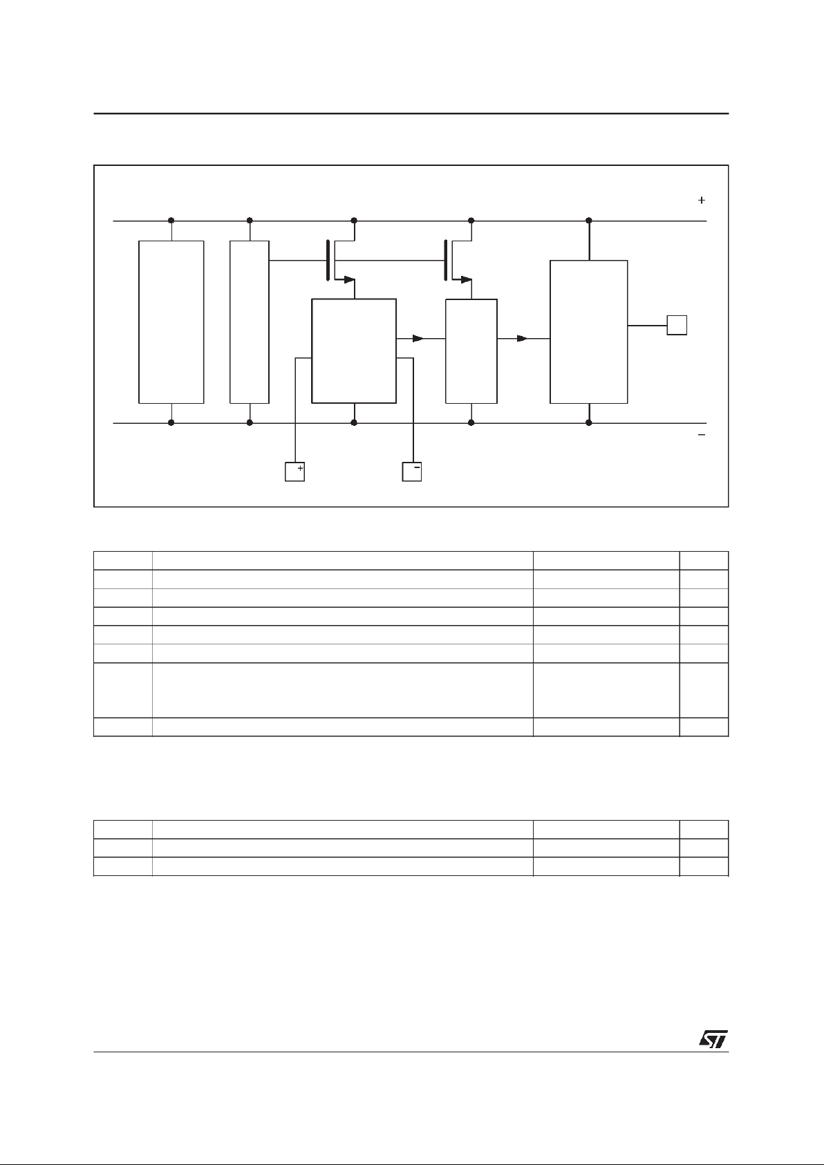
E E
Input
differential
Second
stage
Output
stage
Output
CC
V
CC
V
Current
source
xI
BLOCK DIAGRAM
MAXIMUMRATINGS
Symbol Parameter Value Unit
V
CC
+
Supply Voltage -(note 1) 18 V
V
id
Differential Input Voltage -(note 2) ±18 V
V
i
Input Voltage - (note 3) -0.3 to 18 V
I
O
Output Current for V
CC
+
≥ 15V ±30 mA
I
in
Input Current ±5mA
T
oper
Operating Free-Air Temperature Range
TS27L4C/AC/BC
TS27L4I/AI/BI
TS27L4M/AM/BM
0 to +70
-40 to +125
-55 to +125
o
C
T
stg
StorageTemperature Range -65 to +150
o
C
Notes : 1. All voltage values, except differential voltage, are with respect tonetwork ground terminal.
2. Differential voltages are at the non-inverting input terminal withrespect to the inverting input terminal.
3. The magnitude of the input andthe output voltages must never exceed the magnitude of the positive supply voltage.
OPERATING CONDITIONS
Symbol Parameter Value Unit
V
CC
+
Supply Voltage 3 to16 V
V
icm
Common Mode Input Voltage Range 0 to V
CC
+
- 1.5 V
TS27L4C,I,M
2/9
T
T
25
2
T
17 18
R
T
20
T
21
T
T
23
22
Input
Output
T
24
T
19
V
CC
V
CC
T
26
T
27
T
28
T
29
Input
T
3
T
4
T
5
T
2
T
1
R1
C1
T
7
T
6
T
8
T
9
T
13
T
14
T
11
T
12
T
10
T
16
T
15
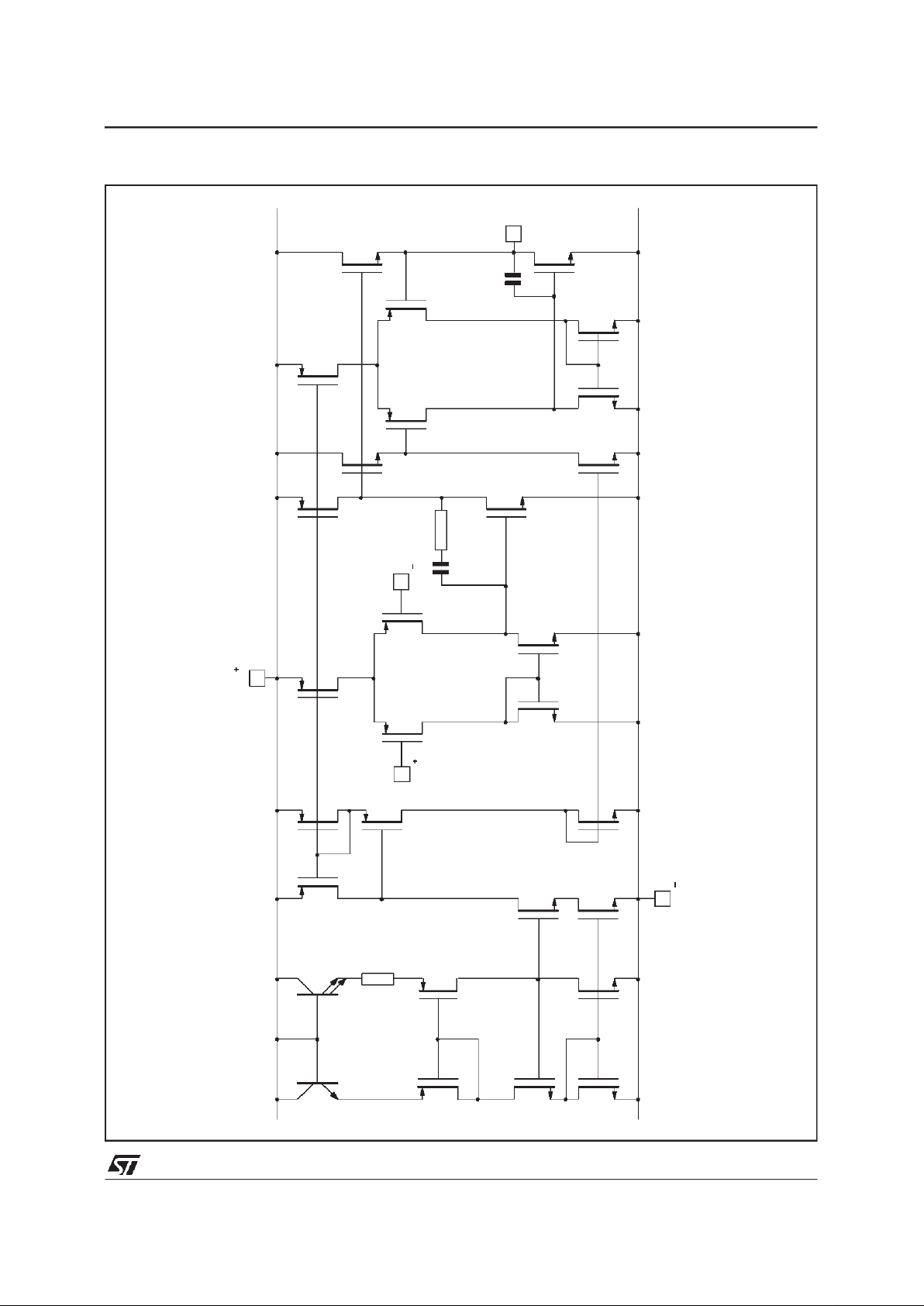
SCHEMATIC DIAGRAM (for 1/4 TS27L4)
TS27L4C,I,M
3/9

ELECTRICAL CHARACTERISTICS
V
CC
+
= +10V,V
CC
-
=0V,T
amb
=25oC (unlessotherwisespecified)
Symbol Parameter
TS27L4C/AC/BC
TS27L4I/AI/BI
TS27L4M/AM/BM
Unit
Min. Typ. Max. Min. Typ. Max.
V
io
Input Offset Voltage
V
O
= 1.4V, Vic= 0V TS27L4C/I/M
TS27L4AC/AI/AM
TS27L4BC/BI/BM
T
min
. ≤ T
amb≤Tmax.
TS27L4C/I/M
TS27L4AC/AI/AM
TS27L4BC/BI/BM
1.1
0.9
0.25
10
5
2
12
6.5
3
1.1
0.9
0.25
10
5
2
12
6.5
3.5
mV
DV
io
Input Offset Voltage Drift 0.7 0.7 µV/oC
I
io
Input Offset Current - (note 1)
V
ic
= 5V, Vo=5V
T
min
. ≤ T
amb≤Tmax.
1
100
1
200
pA
I
ib
Input Bias Current - (note 1)
V
ic
= 5V, Vo=5V
T
min
. ≤ T
amb≤Tmax.
1
150
1
300
pA
V
OH
High Level Output Voltage
V
id
= 100mV, RL=1MΩ
T
min
. ≤ T
amb≤Tmax.
8.8
8.7
9 8.8
8.6
9
V
V
OL
Low Level Output Voltage
V
id
= -100mV 50 50
mV
A
vd
LargeSignal Voltage Gain
V
o
= 1V to 6V, RL=1MΩ,Vic=5V
T
min
. ≤ T
amb≤Tmax.
6045100 6040100
V/mV
GBP Gain Bandwidth Product
Av= 40dB, RL=1MΩ,CL= 100pF
f
in
=10kHz
0.1 0.1
MHz
CMR Common Mode Rejection Ratio
V
o
= 1.4V, Vic= 1V to 7.4V 65 80 65 80
dB
SVR Supply Voltage Rejection Ratio
V
CC
+
= 5V to 10V ,Vo= 1.4V 60 80 60 80
dB
I
CC
Supply Current (per amplifier)
A
v
= 1, no load, Vo=5V
T
min
. ≤ T
amb≤Tmax.
10 15
17
10 15
18
µA
I
o
Output Short Circuit Current
V
id
= 100mV, Vo=0V 60 60
mA
I
sink
Output Sink Current
V
id
= -100mV, Vo=V
CC
45 45
mA
SR Slew-Rate at Unity Gain
R
L
=1MΩ,CL= 100pF, Vi= 3 to 7V 0.04 0.04
V/µs
∅m Phase Margin at Unity Gain
A
v
= 40dB, RL=1MΩ,CL= 100pF 45 45
Degrees
K
ov
Overshoot Factor 30 30 %
e
n
Equivalent Input Noise Voltage
f = 1kHz, R
S
= 100Ω 68 68
nV
√Hz
V
O1/VO2
Channel Separation 120 120 dB
Note : 1. Maximum values including unavoidable inaccuracies ofthe industrial test.
TS27L4C,I,M
4/9

TYPICALCHARACTERISTICS
CC
SUPPLY VOLTAGE, V (V)
T=25
C
A=1
V=V /2
amb
V
2.0
1.5
1.0
0.5
0481216
OCC
CC
SUPPLY CURRENT, I ( A)
Figure 1 : SupplyCurrent(eachamplifier)
versus SupplyVoltage
25 50 75 100 125
INPUTBIASCURRENT,I (pA)
IB
100
10
1
CC
ic
V = 10V
V=5V
amb
TEMPERATURE,T (°C)
Figure2 : Input Bias Current versus Free Air
Temperature
5
4
3
2
1
0
-10 -8 -6 -4 -2 0
amb
id
T=25°C
V = 100mV
V=5V
CC
OH
OUTPUT CURRENT, I (mA)
OUTPUTVOLTAGE,V (V)
OH
CC
V=3V
Figure 3a : High LevelOutputVoltage versus
High Level Output Current
20
16
12
8
4
0
-50 -40 -30 -20 -10 0
amb
id
T=25°C
V = 100mV
V = 16V
CC
OUTPUT CURRENT, I (mA)
OH
OH
OUTPUTVOLTAGE,V (V)
CC
V = 10V
Figure3b : High Level Output Voltage versus
High Level Output Current
1.0
0.8
0.6
0.4
0.2
amb
ic
id
T=25
C
V = 0.5V
V = -100mV
V=3V
V=5V
CC
CC
OL
OUTPUT VOLTAGE, V (V)
0123
OUTPUT CURRENT, I (mA)
OL
Figure 4a : Low Level Output Voltage versus
Low Level Output Current
048121620
OUTPUT VOLTAGE, V (V)
OL
amb
id
i
T=25 C
V = 0.5V
V = -100mV
CC
V=10V
CC
V = 16V
OUTPUT CURRENT, I (mA)
OL
3
2
1
Figure4b : Low Level Output Voltage versus
Low LevelOutputCurrent
TS27L4C,I,M
5/9

TYPICALCHARACTERISTICS (continued)
50
40
30
20
10
0
-10
6
10
10
23
10
4
10
5
10
7
10
GAIN (dB)
PHASE (Degrees)
0
45
90
135
180
FREQUENCY, f(Hz)
T=25
C
V = 10V
R=1M
Ω
C = 10 0pF
A=100
amb
CC
L
L
VCL
PHASE
GAIN
Phase
Margin
Gain
Bandwidth
Produc t
+
Figure 5 : Open Loop Frequency Response and
PhaseShift
0481216
GAIN BANDW. PROD., GBP (MHz)
amb
L
L
V
T=25 C
R=1M
Ω
C = 100pF
A=1
SUPPLYVOLTAGE, V (V)
CC
120
100
80
60
40
Figure6 : GainBandwidthProduct versus
Supply Voltage
60
04 8 1216
SUPPLY VOLTAGE, V (V)
CC
amb
L
L
T=25
C
R=1M
Ω
C = 100pF
A=1
V
PHASE MARGIN, m (Degrees)
φ
50
40
30
Figure 7 : PhaseMargin versus Supply Voltage
80
70
60
50
40
L
CAPACITANCE, C (pF)
PHASE MARGIN, m (Degrees)
φ
200
80
100
6040
T=25 C
R=1M
Ω
A=1
V=10V
amb
L
V
CC
Figure8 : Phase Margin versusCapacitiveLoad
0.05
0.04
0.03
0.02
4 6 8 10 12 14 16
SUPPLY VOLTAGE, V (V)
CC
SLEW RATES, SR (V/
µ
s)
amb
L
L
T=25
C
R=1M
Ω
C = 100p F
SR
SR
Figure 9 : Slew Rates versus Supply Voltage
300
200
100
0
EQUIVALENTINPUTNOISE
VOLTAGE(nV/VHz)
1 10
100 1000
FREQUENCY(Hz)
=10V
=25°C
T
amb
V
CC
=100Ω
R
S
Figure10 : Input VoltageNoise versusFrequency
TS27L4C,I,M
6/9

PM-DIP14.EPS
PACKAGE MECHANICAL DATA
14 PINS- PLASTICDIP
Dim.
Millimeters Inches
Min. Typ. Max. Min. Typ. Max.
a1 0.51 0.020
B 1.39 1.65 0.055 0.065
b 0.5 0.020
b1 0.25 0.010
D 20 0.787
E 8.5 0.335
e 2.54 0.100
e3 15.24 0.600
F 7.1 0.280
i 5.1 0.201
L 3.3 0.130
Z 1.27 2.54 0.050 0.100
DIP14.TBL
TS27L4C,I,M
7/9

PM-SO14.EPS
PACKAGE MECHANICAL DATA
14 PINS- PLASTICMICROPACKAGE(SO)
Dim.
Millimeters Inches
Min. Typ. Max. Min. Typ. Max.
A 1.75 0.069
a1 0.1 0.2 0.004 0.008
a2 1.6 0.063
b 0.35 0.46 0.014 0.018
b1 0.19 0.25 0.007 0.010
C 0.5 0.020
c1 45
o
(typ.)
D 8.55 8.75 0.336 0.334
E 5.8 6.2 0.228 0.244
e 1.27 0.050
e3 7.62 0.300
F 3.8 4.0 0.150 0.157
G 4.6 5.3 0.181 0.208
L 0.5 1.27 0.020 0.050
M 0.68 0.027
S8
o
(max.)
SO14.TBL
TS27L4C,I,M
8/9

PACKAGE MECHANICALDATA
14 PINS- THIN SHRINK SMALL OUTLINEPACKAGE
Dim.
Millimeters Inches
Min. Typ. Max. Min. Typ. Max.
A 1.20 0.05
A1 0.05 0.15 0.01 0.006
A2 0.80 1.00 1.05 0.031 0.039 0.041
b 0.19 0.30 0.007 0.15
c 0.09 0.20 0.003 0.012
D 4.90 5.00 5.10 0.192 0.196 0.20
E 6.40 0.252
E1 4.30 4.40 4.50 0.169 0.173 0.177
e 0.65 0.025
k0
o
8
o
0
o
8
o
l 0.50 0.60 0.75 0.09 0.0236 0.030
Information furnished is believed to be accurate and reliable. However, STMicroelectronics assumes no responsibility for the
consequences of use of such information nor for any infringement of patents or other rights of third parties which may resultfrom
its use. No license is granted by implication or otherwise under any patent or patent rights of STMicroelectronics.Specifications
mentioned in this publication are subject to change without notice. This publication supersedes and replaces all information
previously supplied. STMicroelectronics products are notauthorized for useas criticalcomponents inlife supportdevices or systems
without express written approval of STMicroelectronics.
The ST logo is a trademark of STMicroelectronics
1998 STMicroelectronics – Printed in Italy – AllRights Reserved
STMicroelectronicsGROUP OF COMPANIES
Australia - Brazil - Canada -China - France - Germany - Italy -Japan - Korea- Malaysia - Malta - Mexico - Morocco
The Netherlands - Singapore - Spain - Sweden- Switzerland -Taiwan - Thailand - United Kingdom - U.S.A.
http://www.st.com
ORDER CODE :
TS27L4C,I,M
9/9
 Loading...