

SGS Thomson Microelectronics TS27L4M, TS27L4IN, TS27L4ID, TS27L4I, TS27L4AIN Datasheet
...
TS27L4C,I,M
VERYLOW POWER CMOS
QUAD OPERATIONAL AMPLIFIERS
November 1998
.
ULTRA LOWCONSUMPTIION : 10µA/op
.
OUTPUT VOLTAGE CAN SWING TO
GROUND
.
EXCELLENTPHASE MARGIN ON
CAPACITIVE LOADS
.
STABLE AND LOW OFFSETVOLTAGE
.
THREEINPUTOFFSETVOLTAGE
SELECTIONS
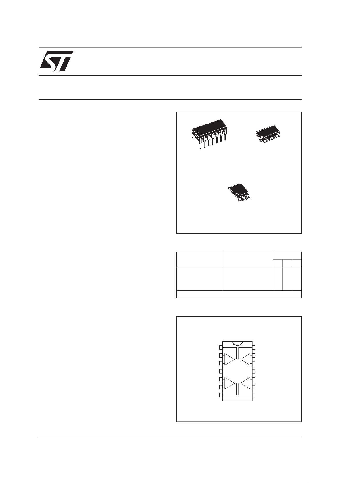
Inverting Input 2
Non-inverting Input 2
Non-inverting Input 1
CC
V
-
CC
V
1
2
3
4
8
5
6
7
9
10
11
12
13
14
+
Output 3
Output 4
Non-inverting Input 4
Inverting Input 4
Non-inverting Input 3
Inverting Input 3
-
+
-
+
-
+
-
+
Output 1
Inverting Input 1
Output 2
PIN CONNECTIONS (top view)
N
DIP14
(Plastic Package)
D
SO14
(Plastic Micropackage)
DESCRIPTION
The TS274 series are low cost, low power quad
operational amplifiers designed to operate with
single or dual supplies. These operationalamplifiers use the SGS-THOMSON silicon gate CMOS
process allowing an excellentconsumption-speed
ratio. These series are ideally suited for low consumption applications.
Three power consumptions are availableallowing
to have always the best consumption-speed ratio:
● I
CC
=10µA/amp.: TS27L4 (very lowpower)
● I
CC
= 150µA/amp. : TS27M4 (low power)
● I
CC
= 1mA/amp. : TS274 (high speed)
These CMOS amplifiers offer very high input impedance and extremely low input currents. The
major advantageversus JFET devices is the very
low inputcurrents driftwith temperature
(see figure2).
ORDER CODES
Part Number
Temperature
Range
Package
NDP
TS27L4C/AC/BC 0
o
C, +70oC ●●●
TS27L4I/AI/BI -40oC, +125oC ●●●
TS27L4M/AM/BM -55oC, +125oC ●●●
Example :TS27M4ACN
P
TSSOP14
(Thin Shrink Small Outline Package)
1/9
E E
Input
differential
Second
stage
Output
stage
Output
CC
V
CC
V
Current
source
xI
BLOCK DIAGRAM
MAXIMUMRATINGS
Symbol Parameter Value Unit
V
CC
+
Supply Voltage -(note 1) 18 V
V
id
Differential Input Voltage -(note 2) ±18 V
V
i
Input Voltage - (note 3) -0.3 to 18 V
I
O
Output Current for V
CC
+
≥ 15V ±30 mA
I
in
Input Current ±5mA
T
oper
Operating Free-Air Temperature Range
TS27L4C/AC/BC
TS27L4I/AI/BI
TS27L4M/AM/BM
0 to +70
-40 to +125
-55 to +125
o
C
T
stg
StorageTemperature Range -65 to +150
o
C
Notes : 1. All voltage values, except differential voltage, are with respect tonetwork ground terminal.
2. Differential voltages are at the non-inverting input terminal withrespect to the inverting input terminal.
3. The magnitude of the input andthe output voltages must never exceed the magnitude of the positive supply voltage.
OPERATING CONDITIONS
Symbol Parameter Value Unit
V
CC
+
Supply Voltage 3 to16 V
V
icm
Common Mode Input Voltage Range 0 to V
CC
+
- 1.5 V
TS27L4C,I,M
2/9
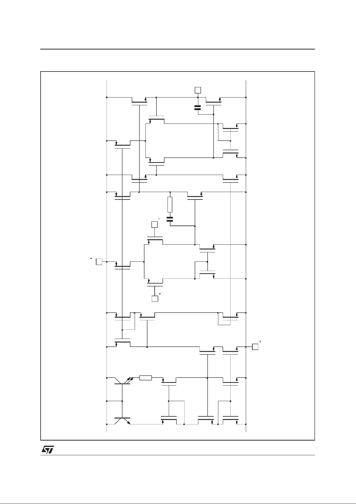
T
T
25
2
T
17 18
R
T
20
T
21
T
T
23
22
Input
Output
T
24
T
19
V
CC
V
CC
T
26
T
27
T
28
T
29
Input
T
3
T
4
T
5
T
2
T
1
R1
C1
T
7
T
6
T
8
T
9
T
13
T
14
T
11
T
12
T
10
T
16
T
15
SCHEMATIC DIAGRAM (for 1/4 TS27L4)
TS27L4C,I,M
3/9
 Loading...