

SGS Thomson Microelectronics TS27L2IN, TS27L2ID, TS27L2I, TS27L2CN, TS27L2CD Datasheet
...
TS27L2C,I,M
LOW POWER CMOS
DUALOPERATIONAL AMPLIFIERS
June 1998
.ULTRALOWCONSUMPTION: 10µA/op
.OUTPUT VOLTAGE CAN SWING TO
GROUND
.EXCELLENTPHASE MARGINON
CAPACITIVELOADS
.STABLEANDLOW OFFSETVOLTAGE
.THREEINPUT OFFSETVOLTAGE
SELECTIONS
1
2
3
45
6
7
8
CC
+
-
-
+
-
+
CC
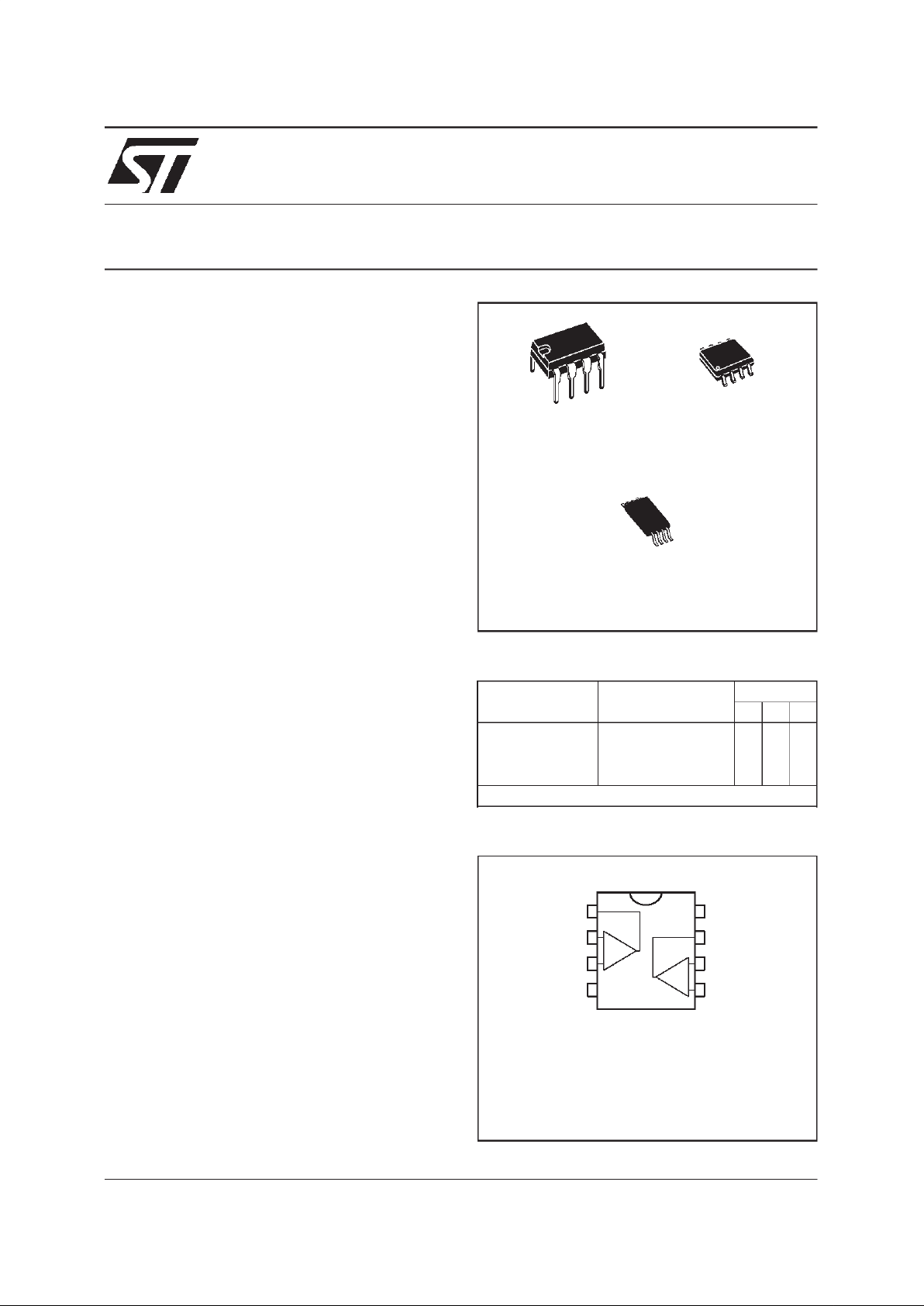
1 - Output 1
2 - InvertingInput1
3 - Non-invertingInput 1
4-V
5 - Non-invertingInput 2
6 - InvertingInput2
7 - Output 2
8-V
PIN CONNECTI O NS (t o p v iew)
N
DIP8
(PlasticPackage)
D
SO8
(PlasticMicropackage)
DESC RIP TI ON
The TS272seriesare low cost, lowpowerdualoperationalamplifiers designedtooperatewith single
or dual supplies. These operationalamplifiers use
the SGS-THOMSONsilicongateCMOSprocessallowing an excellent consumption-speed ratio.
Theseseries areideallysuitedforlowconsumption
applications.
Threepowerconsumptionsareavailableallowingto
have alwaysthe bestconsumption-speedratio :
l ICC = 10mA/amp.: TS27L2 (verylow power)
l ICC=150mA/amp.: TS27M2(lowpower)
l ICC=1mA/amp.: TS272 (highspeed)
TheseCMOSamplifiersofferveryhighinputimpedance and extremelylow input currents.The major
advantageversusJFETdevicesistheverylowinput
currentsdrift with temperature(see figure2).
ORDER CODES
Part Number
Temperature
Range
Package
NDP
TS27L2C/AC/BC 0
o
C, +70oC ●●●
TS27L2I/AI/BI -40oC, +125oC ●●●
TS27L2M/AM/BM -55oC, +125oC ●●●
Example : TS27L2ACN
P
TSSOP8
(Thin ShrinkSmall Outline Package)
1/9
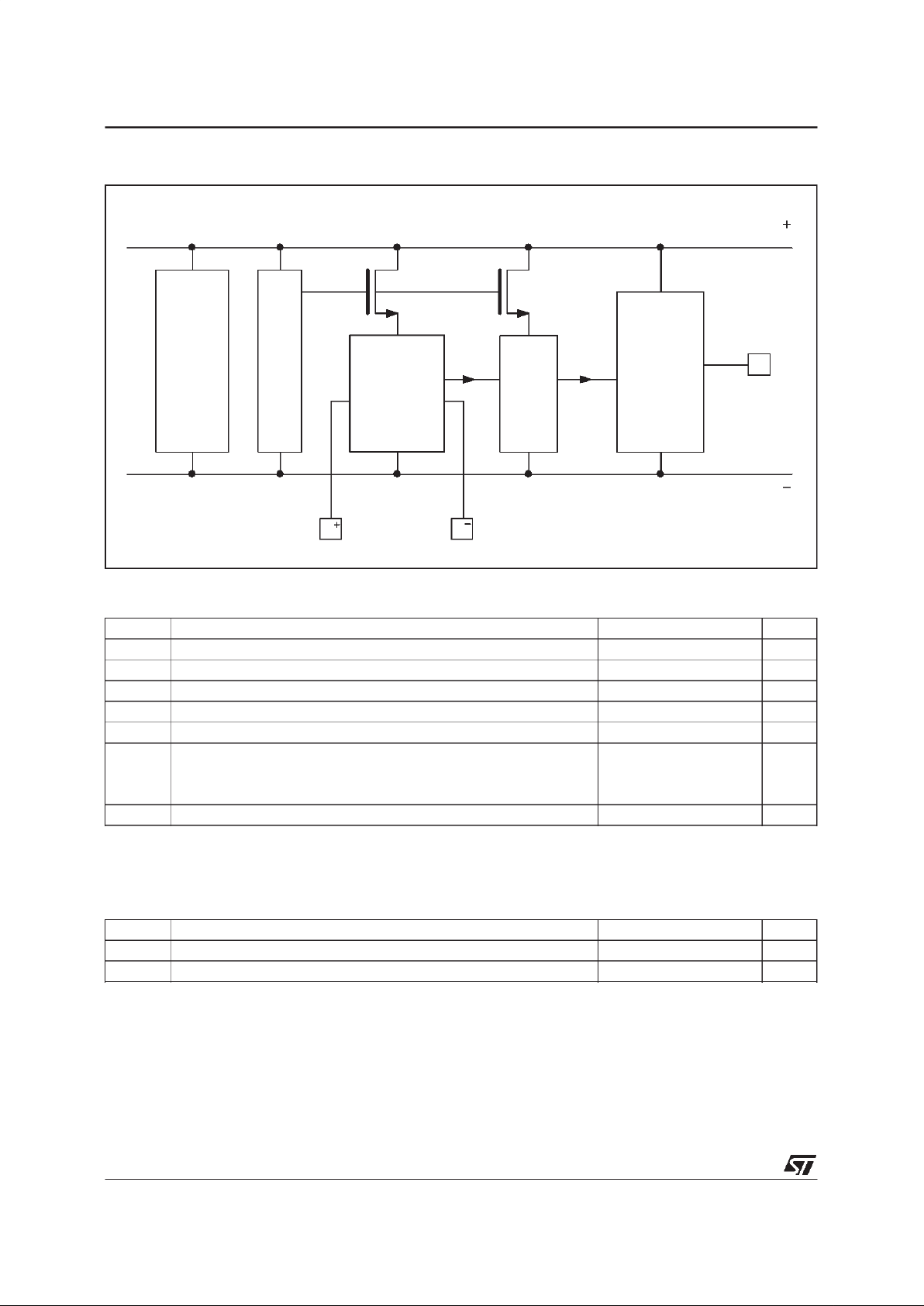
E E
Input
differential
Second
stage
Output
stage
Output
CC
V
CC
V
Current
source
xI
BLOCK DIAGRAM
MAXIMUM RATINGS
Symbol Parameter Value Unit
V
CC
+
Supply Voltage - (note 1) 18 V
V
id
Differential Input Voltage - (note 2) ±18 V
V
i
Input Voltage - (note 3) -0.3 to 18 V
I
O
Output Current for V
CC
+
≥ 15V ±30 mA
I
in
Input Current ±5mA
T
oper
Operating Free-Air Temperature Range
TS27L2C/AC/BC
TS27L2I/AI/BI
TS27L2M/AM/BM
0 to +70
-40 to +125
-55 to +125
o
C
T
stg
Storage Temperature Range -65 to +150
o
C
Notes : 1.All voltage values, exc ept differential voltage, ar e with resp ec t t o network ground t er minal.
2.Di f ferential voltages are at the non- inverting input t ermi nal wi t h respect t o the invert i ng input term inal.
3.The ma gni tude of the input and the outp ut vol t ages must never exceed the magnitud e of the pos itive supply volt age.
OPERATING CONDITIONS
Symbol Parameter Value Unit
V
CC
+
Supply Voltage 3 to 16 V
V
icm
Common Mode Input Voltage Range 0 to V
CC
+
- 1.5 V
TS27L2C,I,M
2/9
T
T
25
2
T
17 18
R
T
20
T
21
T
T
23
22
Input
Output
T
24
T
19
V
CC
V
CC
T
26
T
27
T
28
T
29
Input
T
3
T
4
T
5
T
2
T
1
R1
C1
T
7
T
6
T
8
T
9
T
13
T
14
T
11
T
12
T
10
T
16
T
15
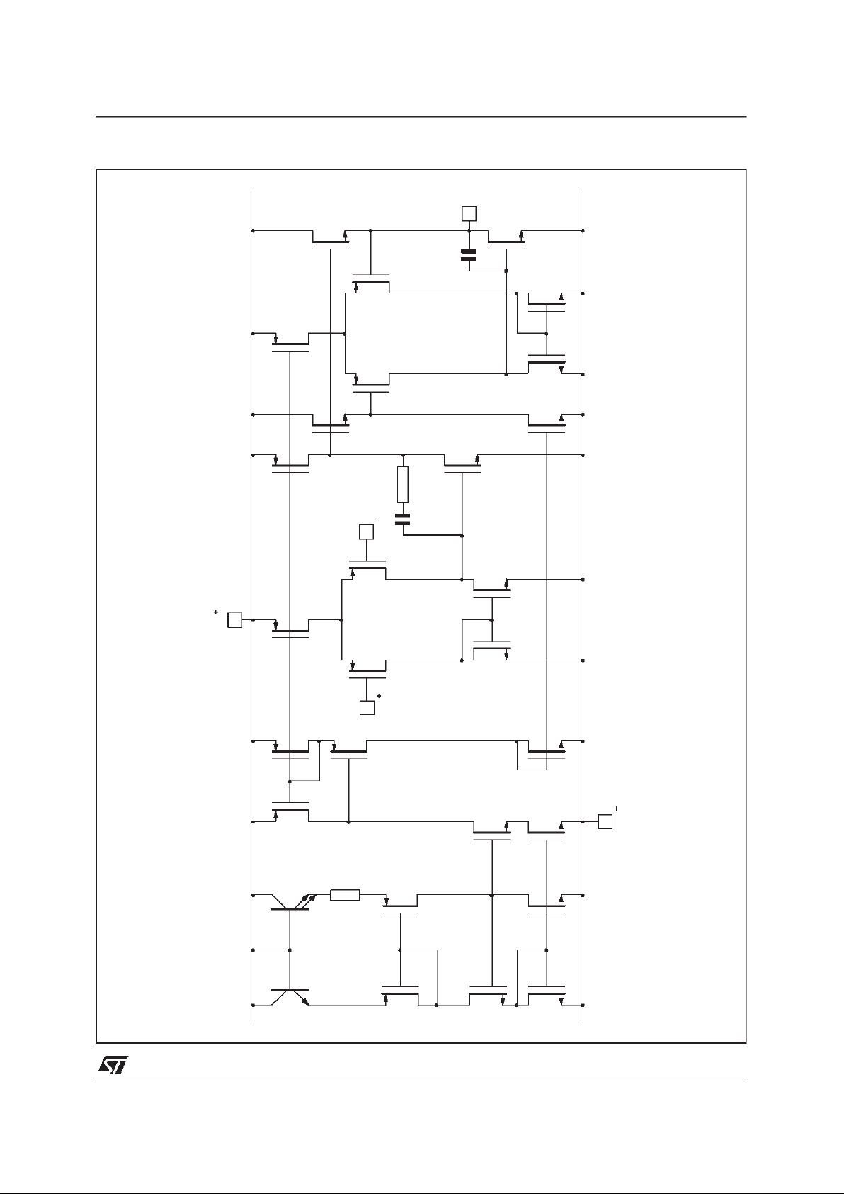
SCHE MATIC DIAGRAM (for 1 /2 TS27L2)
TS27L2C,I,M
3/9
 Loading...