

SGS Thomson Microelectronics TS274CD, TS274CN, TS274C, TS274BIN, TS274BCD Datasheet
...
TS274C,I,M
HIGH SPEED CMOS
QUAD OPERATIONALAMPLIFIERS
October 1997
.
OUTPUT VOLTAGE CAN SWING TO
GROUND
.
EXCELLENTPHASEMARGIN ON
CAPACITIVE LOADS
.
GAIN BANDWIDTH PRODUCT : 3.5MHz
.
STABLE AND LOW OFFSETVOLTAGE
.
THREE INPUTOFFSET VOLTAGE
SELECTIONS
Inverting Input 2
Non-inverting Input 2
Non-inverting Input 1
CC
V
-
CC
V
1
2
3
4
8
5
6
7
9
10
11
12
13
14
+
Output 3
Output 4
Non-inverting Input 4
Inverting Input 4
Non-inverting Input 3
Inverting Input 3
-
+
-
+
-
+
-
+
Output 1
Inverting Input 1
Output 2
PIN CONNECTIONS (top view)
N
DIP14
(Plastic Package)
D
SO14
(Plastic Micropackage)
ORDER CODES
Part Number
Temperature
Range
Package
ND
TS274C/AC/BC 0
o
C, +70oC ●●
TS274I/AI/BI -40oC, +125oC ●●
TS274M/AM/BM -55oC, +125oC ●●
Example : TS274ACN
DESCRIPTION
The TS274 series are low cost, low power quad
operational amplifiers designed to operate with
single or dual supplies.These operational amplifiers use the SGS-THOMSON silicon gate CMOS
processallowing an excellentconsumption-speed
ratio. These series are ideally suited for low consumption applications.
Three power consumptions are available allowing
to have always the best consumption-speedratio:
● I
CC
=10µA/amp.: TS27L4 (very low power)
● I
CC
= 150µA/amp. : TS27M4 (low power)
● I
CC
= 1mA/amp. : TS274 (high speed)
These CMOS amplifiers offer very high input impedance and extremely low input currents.
The major advantage versus JFET devices is the
very low input currentsdrift withtemperature
(see figure2).
1/8
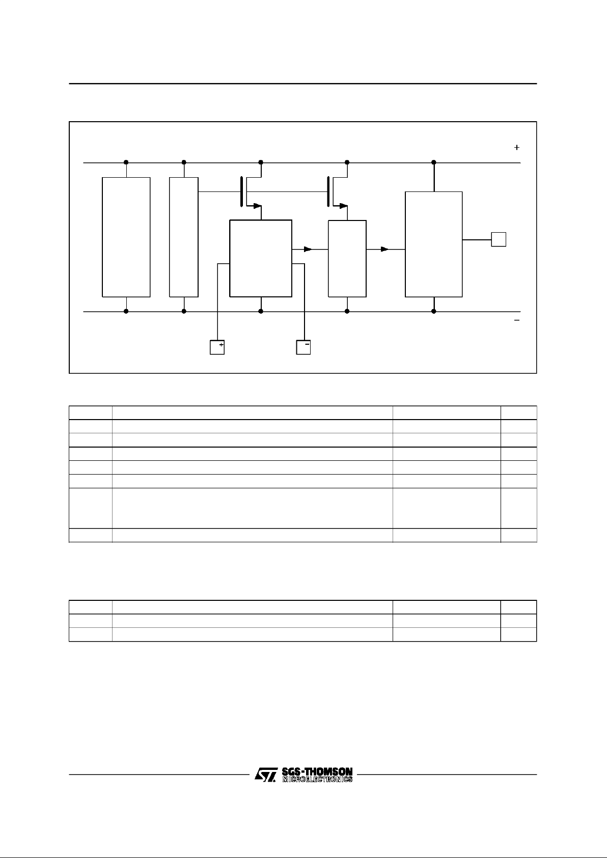
E E
Input
differential
Second
stage
Output
stage
Output
CC
V
CC
V
Current
source
xI
BLOCK DIAGRAM
MAXIMUMRATINGS
Symbol Parameter Value Unit
V
CC
+
Supply Voltage -(note 1) 18 V
V
id
Differential Input Voltage - (note 2) ±18 V
V
i
Input Voltage - (note 3) -0.3 to 18 V
I
O
Output Current for V
CC
+
≥ 15V ±30 mA
I
in
Input Current ±5mA
T
oper
Operating Free-Air Temperature Range
TS274C/AC/BC
TS274I/AI/BI
TS274M/AM/BM
0to+70
-40 to +125
-55 to +125
o
C
T
stg
Storage Temperature Range -65 to +150
o
C
Notes : 1. All voltage values, except differential voltage, are with respect to network ground terminal.
2. Differentialvoltagesare at the non-inverting input terminal with respect to the inverting input terminal.
3. The magnitude of the input and theoutput voltages must never exceed the magnitude of thepositive supply voltage.
OPERATINGCONDITIONS
Symbol Parameter Value Unit
V
CC
+
Supply Voltage 3 to 16 V
V
icm
Common Mode Input VoltageRange 0 to V
CC
+
- 1.5 V
TS274C,I,M
2/8
T
T
25
2
T
17 18
R
T
20
T
21
T
T
23
22
Input
Output
T
24
T
19
V
CC
V
CC
T
26
T
27
T
28
T
29
Input
T
3
T
4
T
5
T
2
T
1
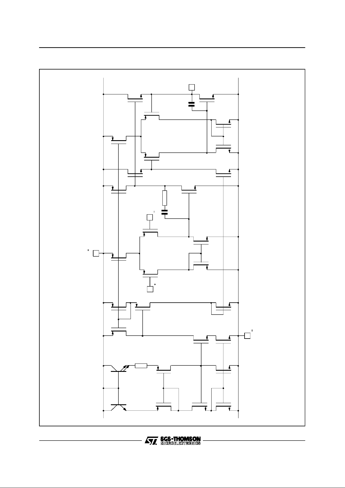
R1
C1
T
7
T
6
T
8
T
9
T
13
T
14
T
11
T
12
T
10
T
16
T
15
SCHEMATICDIAGRAM (for 1/4 TS274)
TS274C,I,M
3/8
 Loading...