

SGS Thomson Microelectronics TS272IN, TS272M, TS272ID, TS272I, TS272CD Datasheet
...
TS272C,I,M
HIGH SPEED CMOS
DUAL OPERATIONAL AMP LIFIERS
August 1998
.
OUTPUT VOLTAGE CAN SWING TO
GROUND
.
EXCELLENT PHAS E MARG IN ON
CAPACITIVE LO ADS
.
GAIN BANDWI DTH PRO DUCT / 3.5MHz
.
ST ABLE AND LOW OFFSET VOLTAGE
.
THREE INPUT OFFSET VOLTAGE
SELECTIONS
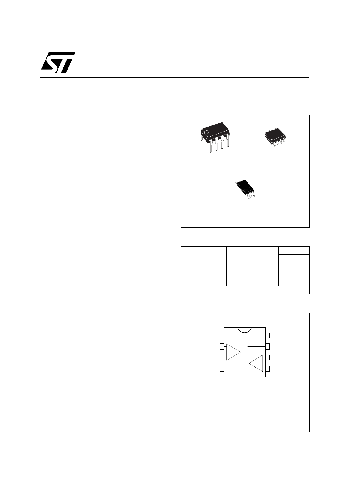
ORDER CODE S
Part Number
Temperature
Range
Package
NDP
TS272C/AC/BC 0
o
C, +70oC ●●●
TS272I/AI/BI -40oC, +125oC ●●●
TS272M/AM/BM -55oC, +125oC ●●●
Example : TS272ACN
N
DIP8
(Plastic Package)
D
SO8
(Plastic Micropackage)
®
1
2
3
45
6
7
8
CC
+
-
-
+
-
+
CC
1 - Output 1
2 - Inverting Input 1
3 - Non-inverting Input 1
4 - V
5 - Non-inverting Input 2
6 - Inverting Input 2
7 - Output 2
8 - V
PIN CONNECTIONS (top view)
DESCRIPTION
The TS272 series are low cost, low power dual
operational amplifiers designed to operate with
single or dual supplies. These operational amplifiers
use the SGS-THOMSON silicon gate CMOS process allowing an excellent consumption-speed ratio.
These series are ideally suited for low
consumption applications.
Three power consumptions are available allowing to
have always the best consumption-speed ratio :
● I
CC
= 10µA/amp. : TS27L2 (very low power)
● I
CC
= 150µA/amp. : TS27M2 (low power)
● I
CC
= 1mA/amp. : TS272 (high speed)
These CMOS amplif iers offer very high input impedance and extremely low input currents. The major
advantage versus JFE T devices is the very low input
currents drift with temperature (see figure 2).
P
TSSOP8
(Thin Shrink Small Outline Package)
1/9

MAXIMUM RATINGS
Symbol Parameter Value Unit
V
CC
+
Supply Voltage - (note 1) 18 V
V
id
Differential Input Voltage - (note 2) ±18 V
V
i
Input Voltage - (note 3) -0.3 to 18 V
I
O
Output Current for V
CC
+
≥ 15V ±30 mA
I
in
Input Current ±5mA
T
oper
Operating Free-Air Temperature Range
TS272C/AC/BC
TS272I/AI/BI
TS272M/AM/BM
0 to +70
-40 to +125
-55 to +125
o
C
T
stg
Storage Temperature Range -65 to +150
o
C
Notes : 1. All voltage values, except diff erential voltage, are with respect to network ground terminal.
2. Differential voltages are at the non-inverting input terminal with respect to the inverting input terminal.
3. The magnitude of the input and the output voltages must never exceed the magnitude of the positive supply voltage.
E
E
Input
differential
Second
stage
Output
stage
Output
CC
V
CC
V
Current
source
x I
BLOCK DIAGRAM
OPERATING CONDITION S
Symbol Parameter Value Unit
V
CC
+
Supply Voltage 3 to 16 V
V
icm
Common Mode Input Voltage Range 0 to V
CC
+
- 1.5 V
TS272C,I,M
2/9

T
T
25
2
T
17 18
R
T
20
T
21
T
T
23
22
Input
Output
T
24
T
19
V
CC
V
CC
T
26
T
27
T
28
T
29
Input
T
3
T
4
T
5
T
2
T
1
R1
C1
T
7
T
6
T
8
T
9
T
13
T
14
T
11
T
12
T
10
T
16
T
15
SCHEMATIC DIAGRAM (for 1/2 TS272)
TS272C,I,M
3/9
 Loading...