

SGS Thomson Microelectronics TS1854ID, TS1854IN, TS1854, TS1852IN, TS1852 Datasheet
...
1/17
■OPERATING AT V
CC
= 1.8V to 6V
■RAIL TO RAIL INPUT & OUTPUT
■EXTENDED Vicm (V
ee
- 0.2V to VCC+ 0.2V)
■LOW SUPPLY CURRENT (120µA)
■GAIN BANDWIDTH PRODUCT (480kHz)
■HIGH STABILITY (able to drive 500pF)
■ESD TOLERANCE (2kV)
■LATCH-UP IMMUNITY
■AVAILABLEIN SOT23-5 MICROPACKAGE
DESCRIPTION
The TS185x (Single, Dual & Quad) is operational
amplifier able to operate with voltages as low as
1.8V and features both Input and Output Rail to
Rail (1.71 @ VCC= 1.8V, RL=2kΩ), 120µA con-
sumption current and 480kHz Gain Bandwidth
Product.
With a such low consumption and a sufficient GBP
for many applications, this Op-Amp is very
well-suited for any kind of battery-supplied and
portable equipment applications.
The TS1851 is housed in the space-saving 5 pin
SOT23-5 package which simplifies the board design (outside dimensions are 2.8mm x 2.9mm).
APPLICATION
■Two-cellbattery-powered systems
■Portable/Battery-powered electronic equipment
■Cordless phones
■Cellular phones
■Laptops
■PDAs
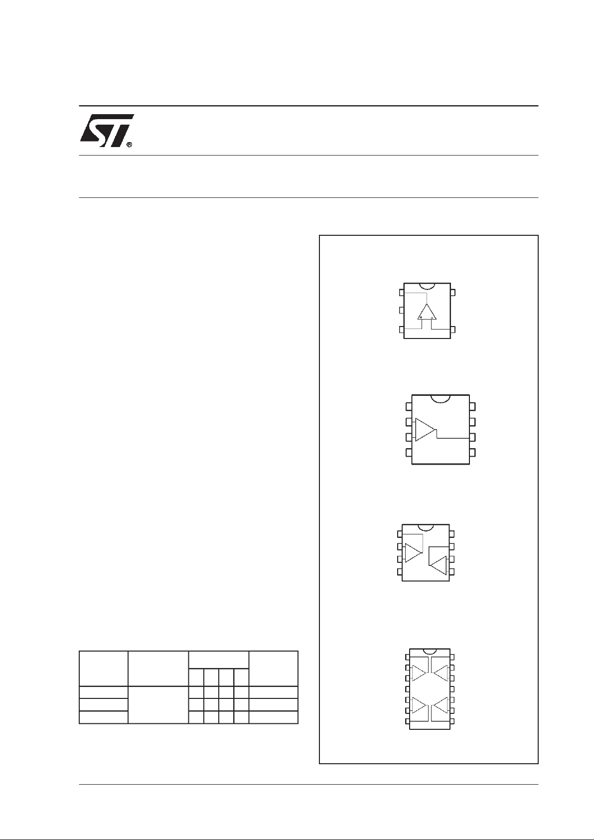
ORDER CODE
N=Dual in Line Package (DIP)
D=Small Outline Package (SO) - also available in Tape & Reel (DT)
P=Thin Shrink Small Outline Package (TSSOP) - only available
in Tape & Reel (PT)
L=Tiny Package (SOT23-5) -only available in Tape & Reel (LT)
PIN CONNECTIONS (top view)
Part
Number
Temperature
Range
Package
SOT23
Marking
NDPL
TS1851I/AI
-40, +125°C
••K161/K162
TS1852I/AI •••
TS1854I/AI •••
1
2
3
4
5
Inverting input
Non-inverting input
Output
V
DD
V
CC
1
2
3
4
5
6
7
8
-
+
Inve rting Input1
N.C.
Non-inve rting Inp ut 1
V
DD
V
CC
Output 2
N.C.
N.C.
Inverting Input 2
Non-inve rting Input 2
Non-inve rting Input1
DD
V
1
2
3
4
8
5
6
7
9
10
11
12
13
14
CC
V
Outp ut3
Outp ut4
Non-inve rting Input4
Inverting Inpu t 4
Non-inve rting Input3
Inverting Inpu t 3
-
+
+
-
+
-
+
Output1
Inve rting Input 1
Output2
1
2
3
45
6
7
8
-
+
-
+
Inve rting Input 1
Output 1
Non-inve rting Input 1
V
DD
V
CC
Output 2
Inverting Input 2
Non-inve rtingInput 2
TS1851ILT
TS1854IN-TS1854ID-TS1854IDT-TS1854IPT
TS1851ID-TS1851IDT
TS1852IN-TS1852ID-TS1852IDT-TS1852IPT
TS1851
TS1852
TS1854
1.8V INPUT/OUTPUT RAIL TO RAIL
LOW POWER OPERATIONAL AMPLIFIERS
May 2000
TS1851-TS1852-TS1854
2/17
ABSOLUTE MAXIMUM RATINGS
OPERATING CONDITIONS
Symbol Parameter Value Unit
V
CC
Supply voltage
1)
7V
V
id Differential Input Voltage
2)
±1V
V
iInput Voltage
3)
-0.3 to VCC+0.3
V
T
oper
Operating Free Air Temperature Range -40 to + 125 °C
T
std
Storage Temperature -65 to +150 °C
T
j
Maximum Junction Temperature 150 °C
R
thjc Thermal Resistance Junction to Case
4)
SOT23-5
DIP8
DIP14
SO8
SO14
TSSOP8
TSSOP14
81
42
32
28
22
26
21
°C/W
R
thja
Thermal Resistance Junction to Ambient - SOT23-5 256 °C/W
ESD Human Body Model 2 kV
Lead Temperature (soldering, 10sec) 260 °C
1. All voltages values, except differential voltage are with respect to network terminal.
2. Differential voltages are non-inverting input terminal with respect to the inverting input terminal.
3. The magnitude of input and output voltages must never exceed V
CC
+0.3V.
4. Short-circuits can cause excessive heating. Destructive dissipation can result from simultaneous short-circuit on all amplifiers
Symbol Parameter Value Unit
V
CC
Supply Voltage 1.8 to 6 V
V
icm
Common Mode Input Voltage Range
1)
Vee-0.2 to VCC+ 0.2
V
V
icm Common Mode Input Voltage Range
2)
Veeto V
CC
V
1. At 25°C, for 1.8 ≤ VCC≤ 6V, V
icm
is extended to Vee- 0.2V, VCC+ 0.2V.
2. In full temperature range, bothRails can be reached when V
CC
does not exceed 5.5V.
TS1851-TS1852-TS1854
3/17
ELECTRICAL CHARACTERISTICS
VCC= +1.8V,Vee= 0V,
T
amb
=25°C (unless otherwise specified)
Symbol Parameter Min. Typ. Max. Unit
V
io
Input Offset Voltage
TS1851/2/4
TS1851A/2A/4A
0.1 3
1
mV
∆V
io
Input Offset Voltage Drift 2 µV/°C
I
io
Input Offset Current
1)
1. Maximum values including unavoidable inaccuracies of the industrial test.
19nA
I
ib Input Bias Current
1)
10 50 nA
CMR
Common Mode Rejection Ratio
0 ≤ V
icm
≤ V
CC
55 85
dB
SVR
Supply Voltage Rejection Ratio
V
icm
= 0.5V
70 80 dB
A
vd
Large Signal Voltage Gain
R
L
= 1OkΩ
R
L
=2kΩ
80
70
100
88
dB
V
OH
High Level Output Voltage
R
L
= 10kΩ
R
L
=2kΩ
1.7
1.65
1.77
1.7
V
V
OL
Low Level Output Voltage
R
L
= 10kΩ
R
L
=2kΩ
40
62
70
90
mV
I
o
Output Source Current
V
ID
= 100mV, VO=V
DD
Output Sink Current
V
ID
= -100mV, VO=V
CC
2
2
29
46
mA
I
CC
Supply Current (per amplifier)
A
VCL
= 1, no load
120 170
µA
GBP
Gain Bandwith Product R
L
= 10kΩ,CL= 100pF, f = 100kHz
300 480 kHz
SR
Slew Rate R
L
= 10kΩ,CL= 100pF, AV= 1
0.1 0.18 V/µs
φm
Phase Margin C
L
= 100pF
60 Degrees
en Input Voltage Noise 40 nV/√Hz
THD Total Harmonic Distortion 0.01 %
TS1851-TS1852-TS1854
4/17
ELECTRICAL CHARACTERISTICS
VCC= +3V,Vee= 0V,
T
amb
=25°C (unless otherwise specified)
Symbol Parameter Min. Typ. Max. Unit
V
io
Input Offset Voltage
TS1851/2/4
TS1851A/2A/4A
0.1 3
1
mV
∆V
io
Input Offset Voltage Drift 2 µV/°C
I
io
Input Offset Current
1)
1. Maximum values including unavoidable inaccuracies of the industrial test.
19nA
I
ib
Input Bias Current
1)
10 55 nA
CMR
Common Mode Rejection Ratio
0 ≤ V
icm
≤ V
CC
60 90
dB
SVR
Supply Voltage Rejection Ratio
V
icm=VCC/2
70 85
dB
A
vd
Large Signal Voltage Gain
R
L
= 1OkΩ
R
L
=2kΩ
83
74
99
90
dB
V
OH
High Level Output Voltage
R
L
= 10kΩ
R
L
=2kΩ
2.9
2.85
2.96
2.94
V
V
OL
Low Level Output Voltage
R
L
= 10kΩ
R
L
=2kΩ
10
46
90
100
mV
I
o
Output Source Current
V
ID
= 100mV, VO=V
DD
Output Sink Current
V
ID
= -100mV, VO=V
CC
2
2
47
47
mA
I
CC
Supply Current (per amplifier)
A
VCL
= 1, no load
150 200
µA
GBP
Gain Bandwith Product R
L
= 10kΩ,CL= 100pF, f = 100kHz
370 600 kHz
SR
Slew Rate R
L
= 10kΩ,CL= 100pF, AV= 1
0.12 0.2 V/µs
φm
Phase Margin C
L
= 100pF
60 Degrees
en Input Voltage Noise 40 nV/√Hz
THD Total Harmonic Distortion 0.01 %
TS1851-TS1852-TS1854
5/17
ELECTRICAL CHARACTERISTICS
VCC= +5V,Vee= 0V,
T
amb
=25°C (unless otherwise specified)
Symbol Parameter Min. Typ. Max. Unit
V
io
Input Offset Voltage
TS1851/2/4
TS1851A/2A/4A
0.1 3
1
mV
∆V
io
Input Offset Voltage Drift 2 µV/°C
I
io
Input Offset Current
1)
19nA
I
ib Input Bias Current
1)
16 63 nA
CMR
Common Mode Rejection Ratio
0 ≤ V
icm
≤ V
CC
65 95
dB
SVR
Supply Voltage Rejection Ratio
V
icm=VCC/2
70 90
dB
A
vd
Large Signal Voltage Gain
R
L
= 1OkΩ
R
L
=2kΩ
85
77
97
93
dB
V
OH
High Level Output Voltage
R
L
= 10kΩ
R
L
=2kΩ
4.85
4.8
4.95
4.91
V
V
OL
Low Level Output Voltage
R
L
= 10kΩ
R
L
=2kΩ
40
80
180
200
mV
I
o
Output Source Current
V
ID
= 100mV, VO=V
DD
Output Sink Current
V
ID
= -100mV, VO=V
CC
2
2
48
48
mA
I
CC
Supply Current (per amplifier)
A
VCL
= 1, no load
162 220
µA
GBP
Gain Bandwith Product R
L
= 10kΩ,CL= 100pF, f = 100kHz
380 630 kHz
SR
Slew Rate R
L
= 10kΩ,CL= 100pF, AV= 1
0.13 0.25 V/µs
φm
Phase Margin C
L
= 100pF
60 Degrees
en Input Voltage Noise 40 nV/√Hz
THD Total Harmonic Distortion 0.01 %
1. Maximum values including unavoidable inaccuracies of the industrial test.
TS1851-TS1852-TS1854
6/17
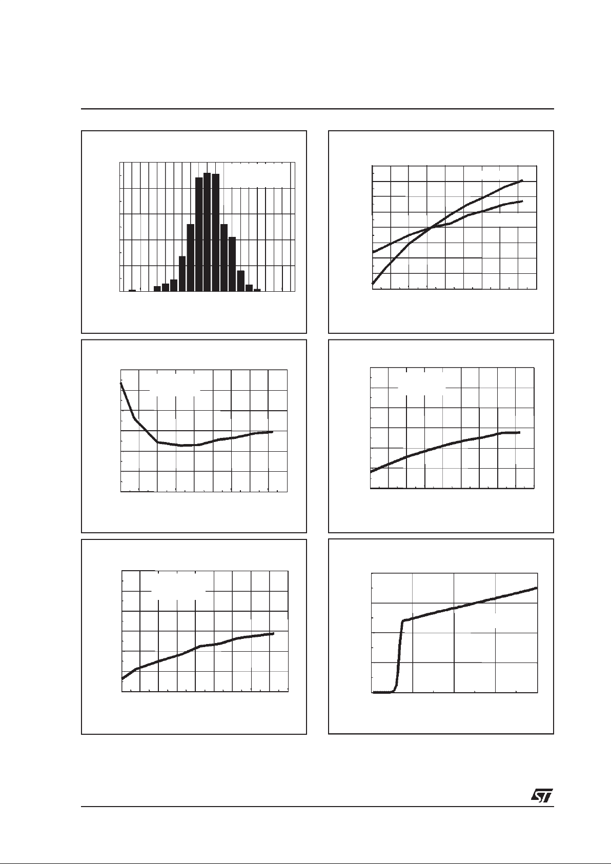
Input OffsetVoltage Distribution
-2. -1.6 -1.2 -.8 -.4 0 .4 .8 1.2 1.6 2
Input Offset Voltage (mV)
0
20
40
60
80
100
Quantity of Pieces
488 pieces tested
Vcc =10V
Temp = +25°C
InputBias Current vs Temperature
-40
-20
0
20
40
60
80
100
120
140
Temperature (°C)
-12
-10
-8
-6
-4
-2
0
Input biascurrent (nA)
Vcc = 1.8V
Vicm = 0.9V
Input Bias Current vs Temperature
-40
-20
0
20
40
60
80
100
120
140
Temperature (°C)
-12
-10
-8
-6
-4
-2
0
Input bias current (nA)
Vcc = 5V
Vicm = 2.5V
Input Offset VoltageDrift vs Temperature
-40
-20
0
20
40
60
80
100
120
140
Temperature (°C)
-400
-300
-200
-100
0
100
200
300
400
Input VoltageDrift (µV)
Vcc = 10V
Vcc = 1.8V
Input Bias Current vs Temperature
-40
-20
0
20
40
60
80
100
120
140
Temperature (°C)
-12
-10
-8
-6
-4
-2
0
Input bias current (nA)
Vcc =3V
Vicm = 1.5V
Supply Current/Amplifier vs Supply Voltage
02468
Supply Voltage (V)
0
50
100
150
200
Supply Current (µA)
Tamb = 25°C
 Loading...