

Datasheet TIP146, TIP140, TIP147, TIP142, TIP145 Datasheet (SGS Thomson Microelectronics)
...
TIP140/141/142
®
COMPLEMENTARY SILICON POWER
■ TIP141, TIP142, TIP145 AND TIP147 ARE
STMicroelectronics PREFERRED
SALESTYPES
■ COMPLEMENTARY PNP - NPN DEVICES
■ MONOLI THIC D A RLING TO N
CONFIGU R ATIO N
■ INTEGRATED ANTIPARALLEL
COLLECTOR-EMITTER DIODE
APPLICATIONS
■ LINEAR AND SWITCHING INDUSTRIAL
EQUIPMENT
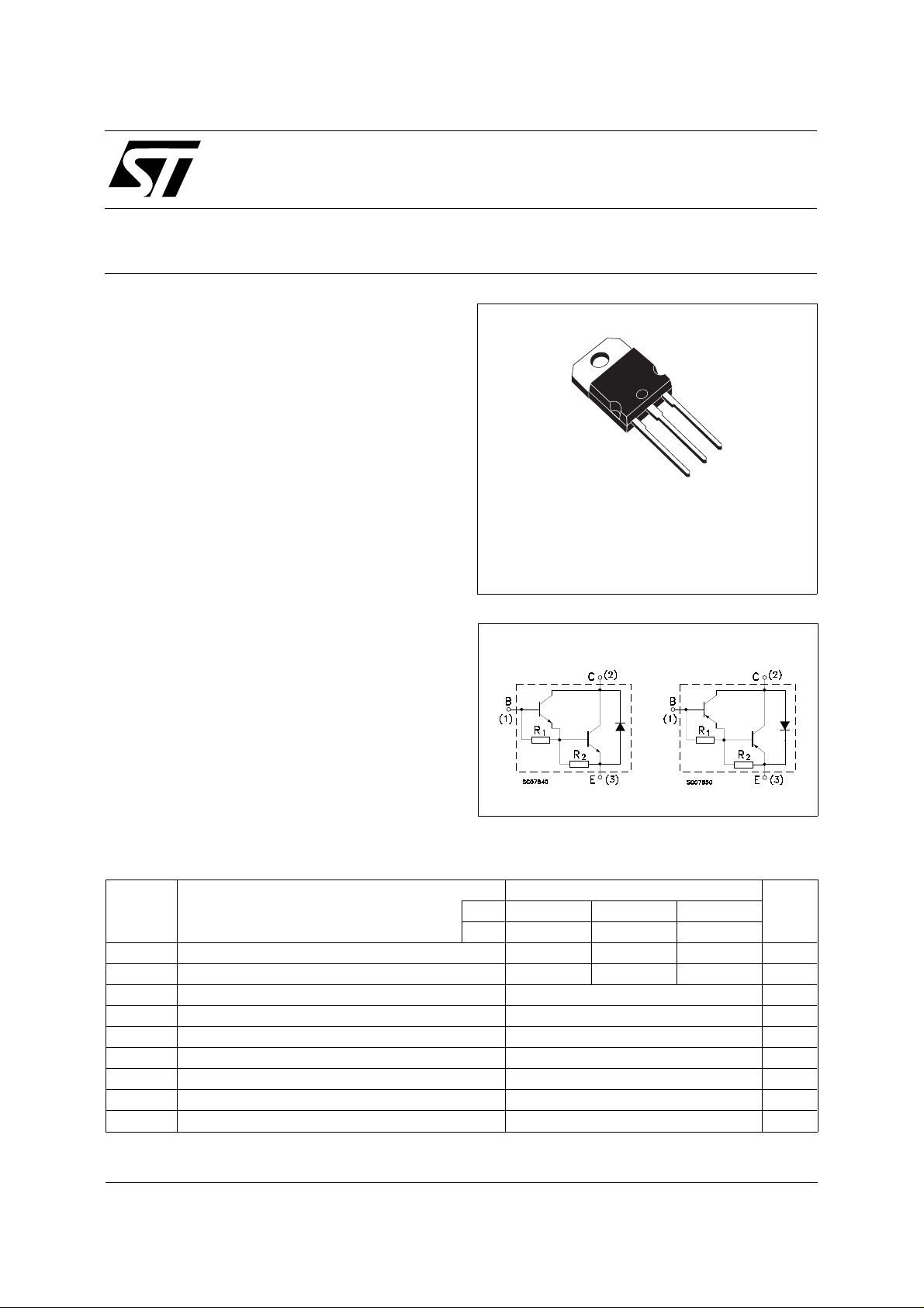
DESCRIPTION
The TIP140, TIP141 and TIP142 are silicon
Epitaxial-Base NPN power transistors in
monolithic Darlington configuration, mounted in
TO-218 plastic package. They are intented for
use in power linear and switching applications.
The complementary PNP types are TIP145,
TIP146 and TIP147 respectively .
TIP145/146/147
DARLINGTON TRANSISTORS
3
2
1
TO-218
INTER NAL SCH E M ATI C DIAG RA M
Typ. = 5 KΩ R2 Typ. = 150 Ω
R
1
ABSOLUTE MAXIMUM RATINGS
Symbol Parameter Value Unit
NPN TIP140 TIP141 TIP142
PNP TIP145 TIP146 TIP147
V
V
V
I
P
T
For PNP types voltage and current values are negative.
March 2000
Collector-Base Voltage (IE = 0) 60 80 100 V
CBO
Collector-Emitter Voltage (IB = 0) 60 80 100 V
CEO
Emitter-Base Voltage (IC = 0) 5 V
EBO
I
Collector Current 10 A
C
Collector Peak Current 20 A
CM
Base Current 0.5 A
I
B
Total Dissipation at T
tot
Storage Temperature -65 to 150
stg
T
Max. Operating Junction Temperature 150
j
≤ 25 oC
case
125 W
o
C
o
C
1/4

TIP140 / TIP141 / TIP142 / TIP14 5 / TIP146 / TIP147
THERMAL DATA
R
thj-case
Thermal Resistance Junction-case Max 1
o
C/W
ELECTRICAL CHARACTERISTICS (T
= 25 oC unless otherwise specified)
case
Symbol Parameter Test Conditions Min. Typ. Max. Unit
I
CBO
Collector Cut-off
Current (I
= 0)
E
for TIP140/145 V
for TIP141/146 V
for TIP142/147 V
I
CEO
Collector Cut-off
Current (I
= 0)
B
for TIP140/145 V
for TIP141/146 V
for TIP142/147 V
I
EBO
V
CEO(sus)
Emitter Cut-off Current
(I
= 0)
C
* Collector-Emitter
Sustaining Voltage
(I
= 0)
B
= 5 V 2 mA
V
EB
I
= 30 mA
C
for TIP140/145
for TIP141/146
for TIP142/147
V
For PNP types voltage and current values are negative.
∗ Pulsed: Pulse duration = 300 µs, duty cycle 1.5 %
* Collector-Emitter
CE(sat)
Saturation Voltage
V
* Base-Emitter Voltage IC = 10 A VCE = 4 V 3 V
BE(on)
h
* DC Current Gain IC = 5 A VCE = 4 V
FE
RESISTIVE LOAD
t
t
on
off
Turn-on Time
Turn-off Time
IC = 5 A IB = 10 mA
I
= 10 A IB = 40 mA
C
I
= 10 A VCE = 4 V
C
IC = 10 A IB1 = 40 mA
= -40 mA RL = 3 Ω
I
B2
= 60 V
CB
= 80 V
CB
= 100 V
CB
= 30 V
CE
= 40 V
CE
= 50 V
CE
60
80
100
1000
500
0.9
4
1
1
1
2
2
2
2
3
mA
mA
mA
mA
mA
mA
V
V
V
V
V
µs
µs
2/4
TIP140 / TIP141 / TIP142 / TIP145 / TIP146 / TIP147
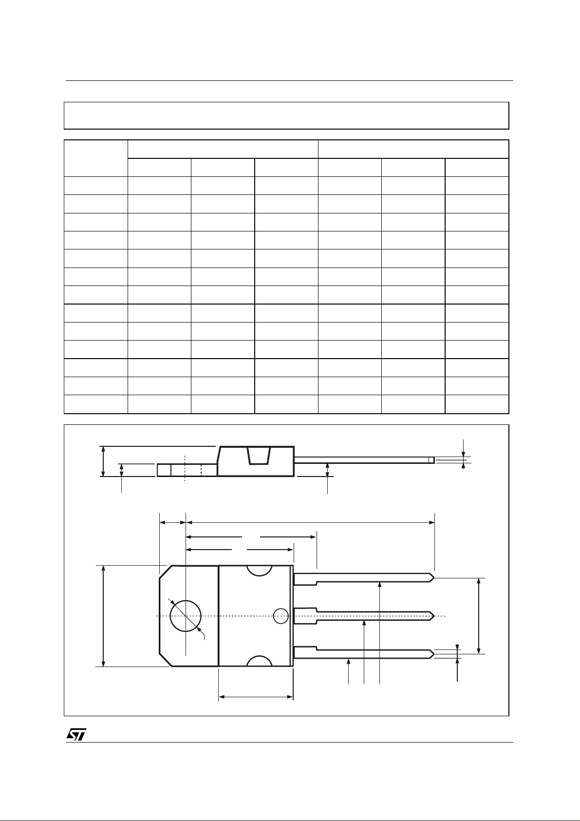
TO-218 (SOT-93) MECHANICAL DATA
DIM.
MIN. TYP. MAX. MIN. TYP. MAX.
A 4.7 4.9 0.185 0.193
C 1.17 1.37 0.046 0.054
D2.5 0.098
E 0.5 0.78 0.019 0.030
F 1.1 1.3 0.043 0.051
G 10.8 11.1 0.425 0.437
H 14.7 15.2 0.578 0.598
L2 – 16.2 – 0.637
L3 18 0.708
L5 3.95 4.15 0.155 0.163
L6 31 1.220
R – 12.2 – 0.480
Ø 4 4.1 0.157 0.161
mm inch
H
A
C
L5
E
D
L6
L3
L2
G
¯
F
R
1
2 3
P025A
3/4

TIP140 / TIP141 / TIP142 / TIP14 5 / TIP146 / TIP147
Information furnished is believed to be accurate and reliable. However, STMicroelectronics assumes no responsibility for the consequences
of use of such inform ation nor for any infringe ment o f patents or other rig hts o f third par ties which ma y resul t from i ts use. N o li cen se is
granted by implicatio n or otherwise under any patent or patent rights of STMicroelectronics. Specification mentioned in this publication are
subject to change without notice. This publication supersedes and replaces all information previously supplied. STMicroelectronics products
are not authorized for use as critical compo nents in life support devices or systems without express written approval of STMicroelectronics.
The ST logo is a trademark of STMicroelectronics
© 2000 STMicroelectro nics – Printed in Italy – All Rights Reserved
STMicroelectronics GROUP OF COMPANIES
Australia - Brazil - China - Finland - France - Germany - Hong Kong - India - Italy - Japan - Malaysia - Malta - Morocco -
Singapore - Spain - Sweden - Switzerland - United Kingdom - U.S.A.
http://www.st.com
4/4
 Loading...