


THDT58S1
THDT58S
ApplicationSpecific Discretes
A.S.D.
FEATURES
CROWBARPROTECTION
DUALASYMMETRICALTRANSIENT
SUPPRESSOR
PEAKPULSE CURRENT:
= 75 A, 10/1000µs for THDT58S.
-I
PP
= 35 A, 10/1000µs for THDT58S1.
-I
PP
HOLDINGCURRENT= 150 mAmin
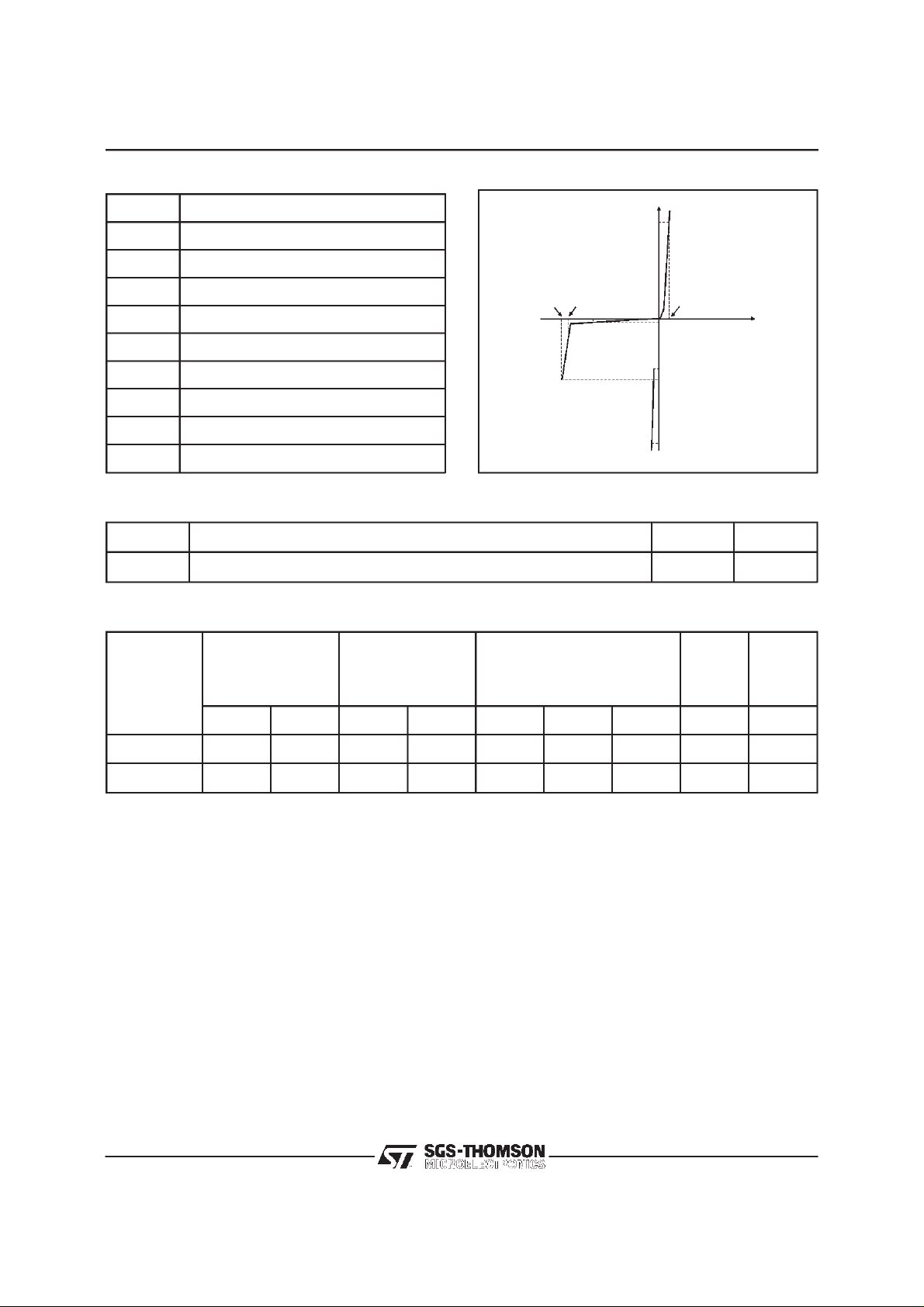
BREAKDOWNVOLTAGE= 58 V.
BREAKOVERVOLTAGE= 80Vmax
DESCRIPTION
This device has been especially designed to
protect subscriber line card interfaces (SLIC)
againsttransientovervoltages.
Its ion-implanted technology confers its excellent
electricalcharacteristics.
This is why this device easily fulfils the main
protection standards which are related to the
overvoltagessuppressionon telecomlines.
The product pinout is compatiblewith TO202 and
TO220packages.
TRANSIENT VOLTAGE SUPPRESSOR
FOR SLIC PROTECTION
SIP3
SCHEMATIC DIAGRAM
NC
Tip
1
2
COMPLIESWITHTHEFOLLOWINGSTANDARDS:
CCITTK20:
VDE0433 : 10/700µs 2kV
VDE0878 : 1.2/50
CNETI3124: 0.5/700µs 1kV
BELLCORE
TR-NWT-001089:
(*)withseries resistors orPTC.
TM: ASD is trademarks of SGS-THOMSON Microelectronics.
February 1998 - Ed: 3
10/700µs 1kV
5/310µs 25A
µs 45/50A(*)
5/200
µs 1.5kV
1/20 µs 40A
0.2/310µs 25A
10/1000µs 1kV
10/1000µs 35/75A(*)
GND
Ring
3
4
1/7

THDT58S / THDT58S1
ABSOLUTE MAXIMUMRATINGS
(T
amb
=25°C)
Symbol Parameter THDT58S1 THDT58S Unit
I
I
TSM
PP
Peak pulsecurrent (seenote 1)
Non repetitivesurgepeak on-state
10/1000µs
8/20 µs
2/10 µs
35
70
80
75
150
t = 20 ms 20 30 A
current (F = 50Hz)
dV/dt Criticalrate of rise of off-state
67%V
BR
5 kV/µs
voltage
T
stg
T
j
T
L
Storagetemperaturerange
Maximumoperatingjunctiontemperature
Maximumleadtemperaturefor soldering
-55 to +150
+150
-40to+150
+150
260 260 °C
during 10s
Note 1 : Pulsewaveform :
10/1000µstr=10µst
5/310µst
2/10µst
=1000µs
=5µst
r
=2µst
r
p
=310µs
p
=10µs
p
100
50
%I
PP
A
°C
°C
0
t
t
rp
THERMAL RESISTANCES
Symbol Parameter Value Unit
(j-a)
R
th
Junctionto ambient
80 °C/W
t
2/7
THDT58S / THDT58S1
ELECTRICAL CHARACTERISTICS
Symbol Parameter
V
RM
I
RM
V
BR
V
BO
I
H
V
I
BO
I
PP
C
Stand-offvoltage
Leakagecurrentat V
Breakdownvoltage
Breakovervoltage
Holdingcurrent
ForwardVoltagedrop
F
Breakovercurrent
Peakpulse current
Capacitance
RM
(T
amb
=25°C)
VBO
VBR
VRM
I
F
I
VF
IRM
IH
IBO
pp
I
V
1 - PARAMETERRELATEDTO THE DIODE LINE/GND
Symbol Testconditions Value Unit
V
IF=5 A tp = 500 µs5V
F
2 - PARAMETERSRELATEDTO THE PROTECTIONTHYRISTOR
Type I
max. min. max. min.
@V
RM
A V V mA V mA mA mA pF
µ
RM
VBR@I
R
VBO@I
note1
BO
max.
I
H
min.
note2
max.
note3
THDT58S 10 56 58 1 80 150 800 150 400
THDT58S1 10 56 58 1 80 50 800 150 200
Note 1 : See thereferencetest circuit 1 for IBOand VBOparameters.
Note 2 : See testcircuit2.
Note 3 : V
= 1V, F= 1MHz.
R
C
3/7

THDT58S / THDT58S1
REFERENCETEST CIRCUIT 1 :
TESTPROCEDURE:
PulseTest duration(tp = 20ms):
-ForBidirectionaldevices= Switch K is closed
-ForUnidirectional devices = SwitchK is open.
V
Selection
OUT
-Devicewith V
-V
- Devicewith V
-V
BO
OUT
BO
OUT
< 200 Volt
=250V
≥ 200Volt
=480V
RMS,R1
RMS,R2
t
=140Ω.
= 240Ω.
FUNCTIONALHOLDING CURRENT (I
) TEST CIRCUIT2
H
R
D.U.T.
V
= - 48 V
BAT
Thisis a GO-NOGOTestwhichallowsto confirm the holdingcurrent (I
testcircuit.
TESTPROCEDURE :
1) Adjustthe currentlevel at theI
2) Firethe D.U.Twith a surgeCurrent: Ipp = 10A , 10/1000µs.
3) TheD.U.Twill comebackoff-state within50 msmax.
valueby short circuitingthe AK of the D.U.T.
H
Surge generator
) levelin a functional
H
-V
P
4/7

THDT58S / THDT58S1
Fig. 1:
Relative variation of holding current
junction temperature.
1.0
0.0
Fig.3: Peakon statevoltageversuspeakon state
current(typicalvalues).
Fig. 2:
Capacitance versus reverse applied
voltage(typicalvalues).
Fig. 4:
Peak forward voltage drop versus peak
forwardcurrent (typicalvalues).
2.0
Fig. 5:
Surge peak current versus overload
duration(THDT58S).
I (A)TSM
40
F=50Hz
Tj initial=25°C
30
20
10
0
1E-2 1E-1 1E+0 1E+1 1E+2 1E+3
t(s)
1.0
Fig. 6:
Surge peak current versus overload
duration(THDT58S1).
I (A)TSM
30
25
20
15
10
5
0
1E-2 1E-1 1E+0 1E+1 1E+2 1E+3
t(s)
F=50Hz
Tj initial=25°C
5/7

THDT58S / THDT58S1
APPLICATION CIRCUIT
TypicalSLIC protectionconcept
RING
GENERATOR
-V
bat
LINE A
PTC
T
E
S
T
R
E
L
A
Y
S
LINE B
PTC
FUNCTIONALDESCRIPTION
Line A
D1
THBTXXX
P1
Tip
RING
RELAY
Line A Protection=
TIP
SLIC
RING
THDT58S
THDT58S1
- For positive Surges versus GND, the
diodeD1 willconduct
- For negative Surges versus GND, the
Protection device P1 will trigger at a
maximumvoltageequal to the V
BO.
6/7
Line B
D2
P2
Line B Protection=
-ForSurgesonlineB, theoperatingmode
is the same,D2 or P2 is activated.
Ring

ORDERCODE
THDT58S / THDT58S1
THDT 58 S 1
35A VERSION
ASYMETRICALTRISIL
BREAKDOWN VOLTAGE
PACKAGEMECHANICAL DATA.
SIP3 Plastic
B
I
a2
b1
Z
e
e3
a1
L
b2
c1
Package:
S = SIP3
MARKING
Type Marking
THDT58S THDT58S
THDT58S1 THDT58S1
DIMENSIONS
REF.
Millimetres Inches
Min. Typ. Max. Min. Typ. Max.
A 7.10 0.280
A
a1 2.80 0.110
a2 1.50 1.90 0.059 0.075
B 10.15 0.400
b1 0.50 0.020
b2 1.35 1.75 0.053 0.069
c1 0.38 0.50 0.015 0.020
e 2.54 0.100
e3 7.62 0.200
I 10.50 0.413
L 3.30 0.130
Z 1.50 0.059
Packaging: Standardpackagingisin antistatictubes
Weight: 0.55g
Information furnished is believed to be accurate and reliable. However,SGS-THOMSON Microelectronics assumes no responsibility for the
consequences of use of such information nor forany infringement of patents or other rights of thirdparties which may result from its use. No
license is grantedby implication or otherwise under any patent or patent rights of SGS-THOMSONMicroelectronics.Specifications mentioned
in thispublication aresubject to change withoutnotice. This publicationsupersedes and replacesall informationpreviously supplied.
SGS-THOMSONMicroelectronics productsare notauthorizedforuse as criticalcomponentsin lifesupport devices or systems withoutexpress
written approval of SGS-THOMSONMicroelectronics.
1998 SGS-THOMSON Microelectronics - Printed in Italy - All rightsreserved.
SGS-THOMSON MicroelectronicsGROUP OF COMPANIES
Australia- Brazil- Canada - China - France- Germany- Italy - Japan - Korea - Malaysia- Malta - Morocco
The Netherlands - Singapore - Spain -Sweden - Switzerland - Taiwan - Thailand - United Kingdom -U.S.A.
7/7
 Loading...