


LOW VOLTAGE
POWER:100mW AT 5V
ANTIDISTORTION SYSTEM FOR LOW CUR-
RENTLINES
TEA7530
MONITORAMPLIFIER
PRELIMINARY DATA
DESCRIPTION
This 8 pins IC is designed for monitor telephone
set andprovides:
a) Signal amplification for monitoring
b) Antidistortionby automaticgain adaptation.
ABSOLUTE MAXIMUM RATINGS
Symbol Parameter
T
V
I
Temperature Range -20 to +70 -20 to +70 °C
op
Supply Voltage 6 6 V
LS
Supply Current for T > 300ms
LS
for T ≤ 300ms
BLOCK DIAGRAM
MINIDIP SO-8
ORDERING NUMBERS:
TEA7530DP TEA7530FP
Value
Minidip SO
90
150
75
120
Unit
mA
mA
June 1993
This is advanced information on anew product now in development or undergoing evaluation. Details are subject to change without notice.
1/11
TEA7530
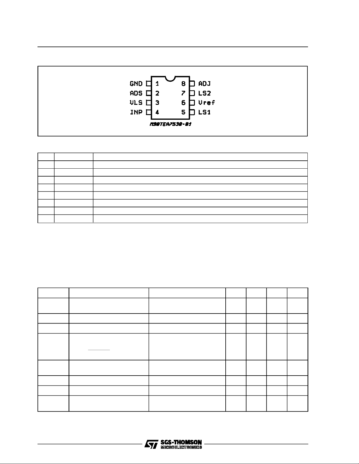
PIN CONNECTION (top view)
PIN FUNCTION
N° Symbol Description
1 GND Ground
2 ADS Antidistortion
3V
LS
4 INP Input Signal
5 LS1 Output Loudspeaker 1
6V
REF
7 LS2 Output Loudspeaker 2
8 ADJ Adjust Internal Reference V
Supply
Internal Reference Voltage
LS
FUNCTIONAL DESCRIPTION
TEA7530performsthe followingfunctions:
The circuit amplifies the incoming signal and
feeds it to the loudspeaker.
ELECTRICAL CHARACTERISTICS (T
=25°C,ILS= 30mA unless otherwise specified)
amb
♦ The Antidistortion system is incorporated for
lowcurrent availablefromline.
♦ The maximum power available on a 50Ω im-
pedanceloudspeakeris 25mW at 3V and 100mW
at5V.
Symbol Parameter Test Condition Min. Typ. Max. Unit
V
LS1
V
LSM
V
ADJ
G Loudspeaker Amplifier
THD Distortion f = 300Hz to 2KHz
Z
INPIN
V
OFFS
GATT Loudspeaker Attenuated
V
Supply ILS = 2mA (fig. 5)
LS1
VLSMaximum I
I
= 30mA (fig. 5)
LS
=40µA (fig. 5; So = closed) 5.7 V
pin8
2.7 3
3.15
3.3
3.4
Voltage Pin 8 ILS= 2 to 30mA (fig. 5 1.0 1.25 1.5 V
ILS= 30mA (fig. 6) 30 32 34 dB
V
− V
(5)
Gain =
(7)
V
(4)
2%
V
(5)-V(7)
= 0.8Vrms; (fig. 6)
Earphone Input (fig. 7) 2.1 2.8 3.5 KΩ
Output Offset [V
Gain = [V
(5)-V(7)
] (fig. 6) -80 80 mV
(5)-V(7)
V
]/V
= 0.7V; (fig. 8)
(2)
V
(4)
= 0.4V; (fig. 8) 20
(2)
-30
30
-20 dB
V
V
dB
2/11
TEA7530
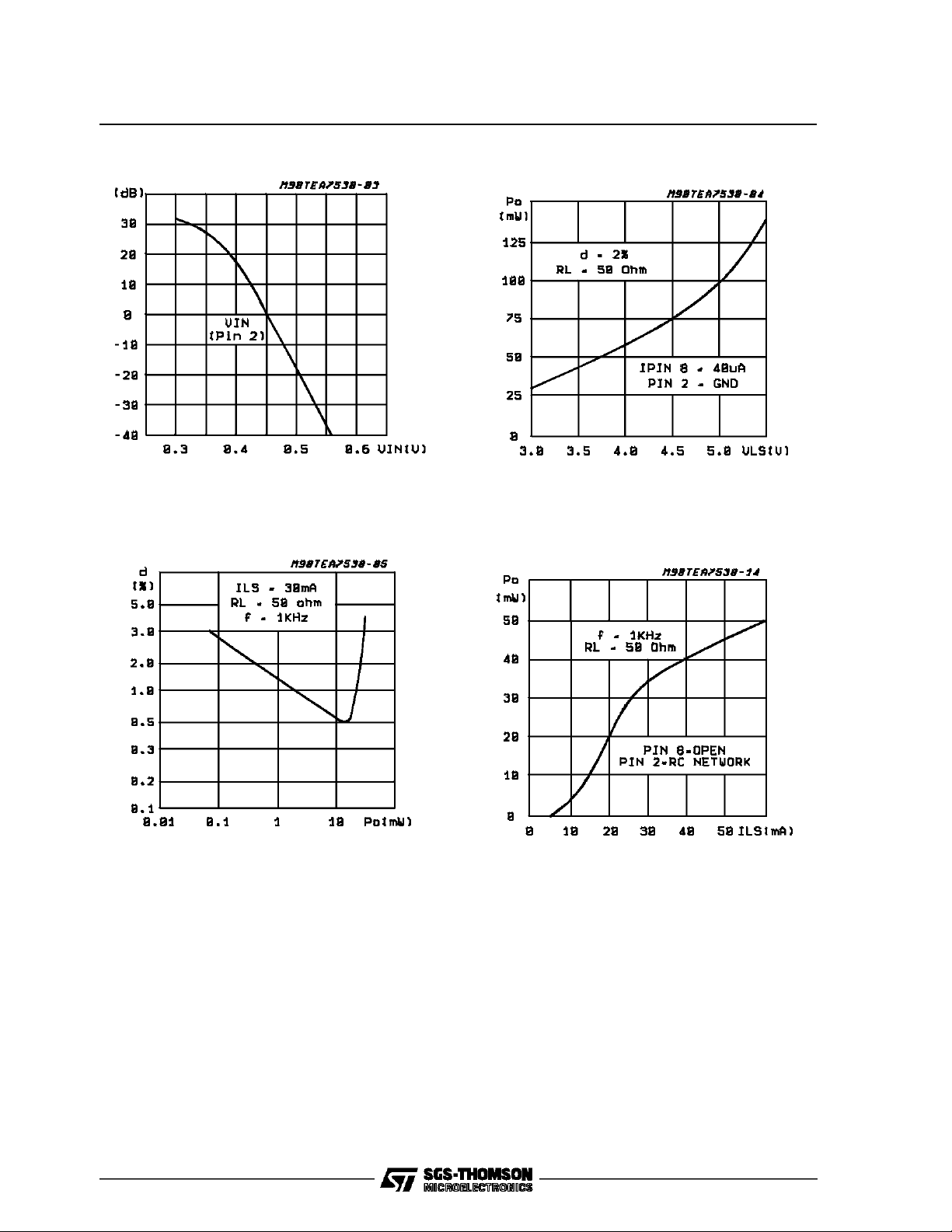
Figure1: LoudspeakerGainvs. Voltage on Pin 2 Figure 2: Power Available on Loudspeakervs.
TypicalCurve. (VoltageMode
V
LS
Figure3: Distortion vs. OutputPower Figure4:
OutputPower vs. SupplyCurrent
(CurrentMode Supply)
3/11
TEA7530
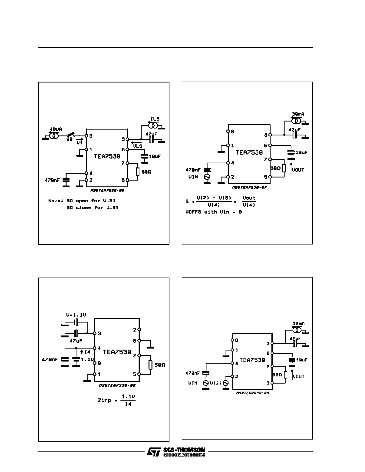
TEST CIRCUITS
Figure5: ShuntvoltageRegulator/ Reference
Voltageat Pin 8.
Figure6: LoudspeakerAmplifier:
Gain/Distortion/OutputOffset
Figure7: Impedance, ZINP
Figure8: Anti-loadingFeedbackSystemat
G = GATT
4/11
 Loading...