

LOW-RANGE PHONE DEDICATED CHIP
.
RING
- GENERATION OF 8 MELODYTONES
(Includingthe 3 GermanMelody Tones)
- 4 STEPS DIGITAL CONTROL ON THE AMPLIFIEROUTPUT LEVEL
.
SPEECH
- TRANSM I TGAINEXTERN ALLYADJUST ABL E
- RECEIV IN GGAINEXTER NALLYADJUSTA B LE
- AGCSLOPEEXTERN A LLYPROGRAMM ABLE
- SOFTCLIPPINGON SENDING CHANNEL
- RECEIVE AMPLIFIER FOR PIEZO OR
ELECTRODYNAMIC TRANSDUCER
- +6dB MODE ON RECEIVECHANNEL
- LINE POWER MANAGEMENT
.
DIALING
- DTMF GENERATOR
- LOW DC MASK DURING MAKE PERIOD
THROUGH MICROCONTROLLER SERIAL
BUS INTERFACE
.
MICROCONTROLLER INTERFACE
- 1.79MHzCLOCKOR3.58MHzOSCILLATOR
INPUT
.
MICROCONTROLLER POWER SUPPLY
.
MICROCONTROLLER CONTROL INTERFACE INCLUDING SERIALBUS
.
LINE CURRENT EXTRACTOR FOR SUPPLY
OF EXTERNAL PERIPHERALS
(Plastic Package)
ORDER CODE : TEA7089AFP
PIN CONNECTIONS
SOFT
RECIN
SN
AGC
1
2
3
4
TEA7089A
SO28
28
27
26
25
DTMF
V
REF
V
RMC
DCL
DESCRIPTION
The TEA7089A is a Telephone Analog Front End
device, TAFE, which integrates the three basic
functionsof a standardtelephoneset :
- Speechnetwork,
- DTMF generator,
- Ringer generatoron buzzer.
A complete telephone set can be designed using
TEA7089A associated with a low cost microcontroller.
June 1998
MIC1
MIC2
GTR
V
GND
IVLS
V
V
V
GREC
5
6
7
8
CC
9
10
11
S
12
L
13
MC
14
24
23
22
21
20
19
18
17
16
15
DATA
MSK
OSC
RI
PON
RES
V
RING
BUZ
EAR+
EAR-
7089A-01.EPS
1/17

TEA7089A
SPEECH
Thespeech network includes :
- a lownoisetransmitchannel suitablefor anykind
of microphonetransducer. Softclippingon transmit line signal is provided by the chip.
- a low noise receive channel with symmetrical
outputs to be compatiblewith both piezoceramic
and electrodynamicearpiece. An additional 6dB
RINGER
Up to 8 different tones can be generated by the
TEA7089Aringer.The digitalvolume controlof the
ringer can be performed through a specific command(4 steps).A ringindicationsignal is provided
to the microcontroller by the TEA7089A.If more
tones are requested the input RM/MSK allows to
inject tones generatedby the microcontroller.
gain can be inserted in the receive channel
throughsoftware control.
- a linelengthgain control(AGC)withstartingpoint
ofgainregulationfixedat25mAlinecurrent;slope
of gainregulationis externallyadjustablewithone
resistor.AGCcan beremovedbyhardware(maximumgain flat) or by software(-2dBflat).
The phoneimpedanceand sidetone can be tuned
throughexternal networks.
FURTHERADVANTAGES
The microcontroller power supply is provided by the
TEA7089A.Thepowersupplyisspecif i cal l ydesigned
tocopewitha longflas horalonggroundkeyduration.
The TEA7089A is able to supply the necessary
current to an external speakerphone circuit
TEA7540 and loudspeaker amplifier TEA7532
without any additionalcircuitry.
Line current and reset indications are provided to
DTMF GENERATOR
The onboard DTMF generator fullfils the CEPT
requirementswith an externalsinglepole filter.
the microcontrollerby theTEA7089A.
The microcontroller drivesthe TEA7089Athrough
a 2 wires serial interface.
PIN DESCRIPTION
Name Pin N° Description
SOFT 1 Transmit Softclipping Time Constant
RECIN 2 Receiving Input
SN 3 Sidetone Network Input
AGC 4 Line Current Regulation Stop Value
MIC1 5 Microphone Input
MIC2 6 Microphone Input
GTR 7 Transmit Gain Adjustment
V
CC
GND 9 Ground
IVLS 10 Line Current Source Power Supply
V
S
V
L
V
MC
GREC 14 Receive Gain Adjustment
EAR- 15 Negative Earphone Output
EAR+ 16 Positive Earphone Output
BUZ 17 RingerBuzzer Output
VRING 18 Ring Power Supply
RES 19 Reset
PON 20 Power On
RI 21 Ring Indicator
OSC 22 Oscillator Input
MSK 23 Mask, Ring Melody Input
DATA 24 Data Input
DCL 25 DataClock Input
V
RMC
V
REF
DTMF 28 DTMF Filter
2/17
8 Transmit and Receive Part Power Supply
11 Voltage Stabilizer
12 Positive Line
13 Unregulated Microcontroller Power Supply
26 Microcontroller Stabilized Power Supply
27 Reference Voltage (VCC/2)
7089A-01.TBL
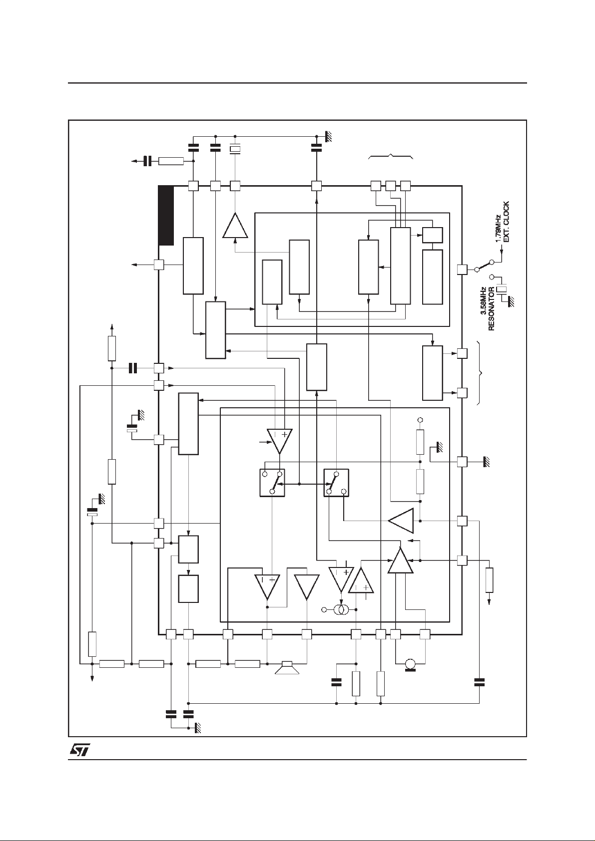
Figure1 : Block Diagram
TEA7089A
CC
V
Sidetone
C30
R13
To Line
To µP
C12
C1
R40 + R15
TEA7089A
RI
21
2
RECIN SN
IVLSV
C15
C16
V
18
SUPPLY
RING POWER
LINE CURRENT
POWER SUPPLY
RMCVRING
26
BUZZER
SUPPLY
LOGIC POWER
BUZ
17
AMPLIFIER
& AGC
SIDETONE
MUTE
AGC
RING
CONTROL
C10
MC
V
13
GENERATOR
SERIAL
REGULATOR
To µP
MSK
DCL
232425
DTMF
GENERATOR
DATA
µP
INTERFACE
REF
V
OSCILLATOR /2
CONTROL
PON & RESET
OSC
1920 22
To µP
PON RES
GND
9
To Line
C8
R10
R11
CC
V
L
R12
12 8 310
S
V
C11
MUTE
DTMFAGC
28
567
MIC1
AGC
MIC2
Microphone
4
R25
CC
V
C3
C3
KVL
SOFT
R4
IN
V
1
GTR
R8
VSTAB
Earphone
Amplifier
EAR-
Earphone
-1
15
REF
V
11
27
REF
V
R14
14
GREC
16
EAR+
R17
C14
7089A-02.EPS
3/17
TEA7089A
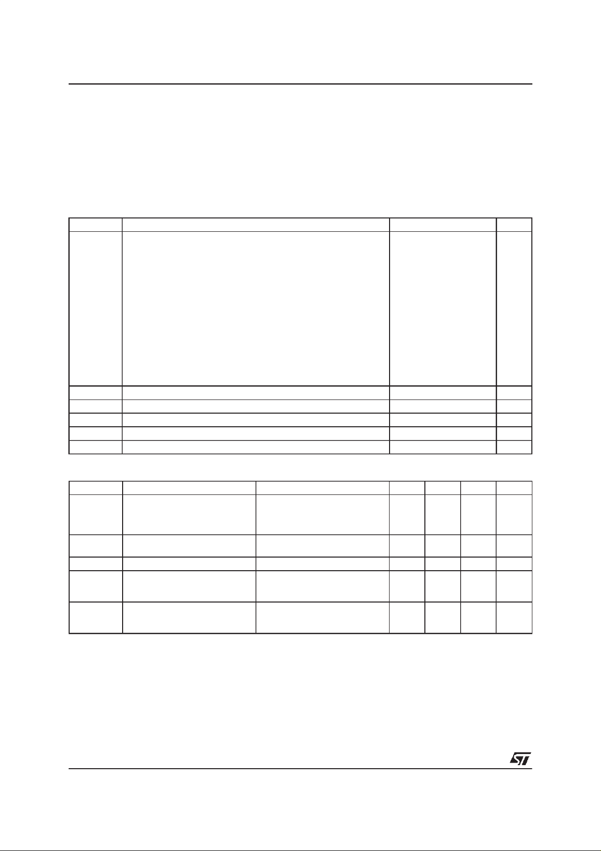
ELECTRICALCHARACTERISTICS
Theblock diagram is given in Figure 1.
Thevalues of the differentnetworks used in this datasheetare defined as followed:
- The return loss is adjusted by R10 of 600Ω.
- The transmitadjust gainnetworkR8 is calculatedinorder to havea gainof46dB typicalwith I
- The sidetone networkZST is set to be lower than 20dB (Vear/Vmic)on a 600Ωloadon line.
- The DC characteristicsare setby a resistorof 82kΩ betweenV
and VS.
L
Absolute MaximumRatings
Symbol Parameter Value Unit
I
LINE
I
RING
T
T
oper
stg
T
Authorized Voltage on
Pin 2 - RECIN
Pin 3 - SN
Pin 8 - V
Pin 10 - IVLS
Pin 12 - V
Pin 13 - V
Pin 17 - BUZ
Pin 18 - V
Pin 19 - RES
Pin 20 - PON
Pin 21 - RI
Pin 22 - OSC
Pin 23 - MSK
Pin 24 - DATA
Pin 25 - DCL
Pin 26 - V
CC
L
MC
RING
RMC
V
V
V
V
V
V
V
V
RING
RMC
RMC
RMC
RMC
RMC
RMC
RMC
Line Current 120 mA
Ring Current 50 mA
Operating Temperature -25, +70 °C
Storage Temperature -55, +150 °C
Junction Temperature -25, +150 °C
j
13
12
11
6
12
6
+0.3, GND -0.3
27
+0.3, GND -0.3
+0.3, GND -0.3
+0.3, GND -0.3
+0.3, GND -0.3
+0.3, GND -0.3
+0.3, GND -0.3
+0.3, GND -0.3
5
LS
=22mA.
V
V
V
V
V
V
V
V
V
V
V
V
V
V
V
V
7089A-02.TBL
DC Characteristics(T
=25°C; Logic in Default Modeunless otherwise noted)
amb
Symbol Parameter Test Conditions Min. Typ. Max. Unit
V
I
VRMC
V
RMC
I
VMC
I
LS
L
Line Voltage
- In Speech and DTMF Mode
- In Mask Mode
Stabilized Supply Voltage
- Output Current
- Output Voltage IRMC = 1.5mA 3.15 3.35 3.55 V
Unstabilized Supply Voltage
- Start up Current
- Output Current
Line Current Source Supply Test 1,VLS=0V;VMC= 3.6V
Test 1
= 22mA
I
L
= 90mA
I
L
= 22mA
I
L
Test 1, IL= 22mA
V
MC
V
MC
= 22mA
I
L
= 90mA
I
L
= 22mA
L
= 2.5V, I
= 3.6V, I
Test 1, I
VRMC
VRMC
= 1.5mA
= 0mA
4
6.7
4.6
7.5
5.2
8.3
3
1.5 mA
10 15
3
10
67
14
75
18
82
Theline current sourcesupply dependsof IL:
- For I
- For I
Onthis pin the maximumoutput levelis : V
4/17
< 20mA: ILS(mA)= 0.765 x IL(mA)- 1.4mA
L
> 20mA: ILS(mA)= 0.92x IL(mA)- 4.5mA
L
10=V12
- (1.2+ 10 x ILS) and V10<6V
V
V
V
mA
mA
mA
mA

TEA7089A
ELECTRICALSPECIFICATIONS(continued)
AC Characteristics(T
Symbol Parameter Test Conditions Min. Typ. Max. Unit
R1 Return Loss Test 2, I
TransmitCharacteristics
(T
=25°C; RL= 600Ω ; f = 1kHz ; Logicin Default Mode unlessotherwisenoted)
amb
Symbol Parameter Test Conditions Min. Typ. Max. Unit
Gtx
Gtxl
Gtxs
Zmic Microphone Input Impedance between MIC1 & MIC2 32 40 48 kΩ
Ntx Noise Test 3, 2kΩ on microphone inputs,
Mmic Microphone Mute Test 3, V
Dtx
V
Max.
L
Microphone Gain Test3, V
Soft Clipping
- Distortion
- Maximum Level on Line
=25°C;RL= 600Ω ; Logic in Default Mode unless otherwisenoted)
amb
= 22mA
f = 300/3400Hz, V
R8 = 1.3kΩ, R25 = 3.9kΩ
I
Test 3, I
L
= -55dBV
m
= 22mA
I
L
= 90mA
I
L
= 22mA
L
= -55dBV, IL= 22mA 60 dB
m
= 22mA, see Figure 2
L
= -41dBV
V
m
= -34dBV 1.5
V
m
= -10dBV
AC
17 dB
4538464047
42
-76 dBmp
2%
dB
dB
Vp
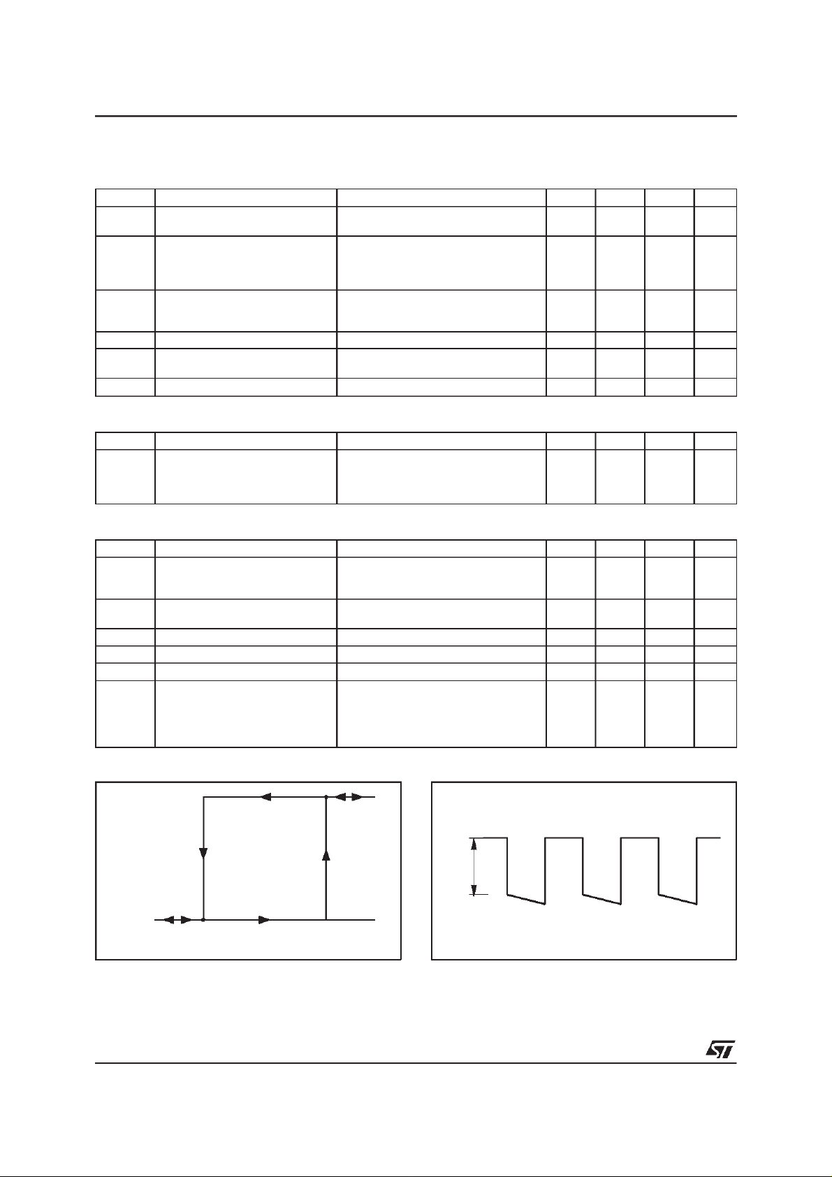
Figure2 : Softclipping
10
Threshold
Level
1
peak on line (V)
AC
V
0.1
0.1 1 10 100
V
microphon e
peak(mV)
Figure3
10
8
6
4
(Pin 12) (V)
L
V
2
VACpeak
0
0 20 406080100
IL(mA)
-15
-10
-5
-2
VACpeak
The maximum gain Gtl is adjustable between 44
and 56dB with R8 :
Gtxl = 20log
820 ⋅
R10 // R
R8 // 50k
+ R11
L
Ω
TheAGCvariationisprogrammedwithoneresistor
connected on Pin AGC. I
is the line current at
SL
whichthe gain must be decreasedby 6dB.
R25 (Ω) =
I
SL
300
− 5mA
For line current lower than I
The transmit and receive gains have a constant
7089A-03.EPS
value.
(R25 > 2.6kΩ)
or higher than ISL,
LL
If no resistor or a resistor higher than 300kΩis
connected on Pin AGC, the gain is constant and
equal to Gtxl and Grxl.±0.5dB.
AGC can be inhibited also through MCU code
”010100”. In this case Tx and Rx gains are fixed
2dB lower than the maximumgain.
The minimumsaturationvoltageof theTEA7089A
respect to ground is 2.2V. On long line, when the
voltage over TEA7089A is low, the softclipping
function automatically limits the AC dynamic to
avoidto reachthe 2.2Vlimiton TEA7089Arespect
7089A-04.EPS
to ground.
5/17
TEA7089A
ELECTRICALSPECIFICATIONS(continued)
ReceiveCharacteristics (T
Symbol Parameter Test Conditions Min. Typ. Max. Unit
E
G
G
Dr Distortion Test 4, Rear = 300Ω,I
Nr Noise Test 4, I
Vear
(010010)
Zout Output Impedance 20 Ω
Sidetone
ff
Eff = (Vear
Gain in Symmetric Mode
Grx = (Vear
RXl
RXs
+
- Vear-) /Vm
+
- Vear-)/V
Earphone Mute I
=25°C; RL=660Ω ; f = 1kHz)
amb
Test 3, V
R14 = 10kΩ, R17 = 15kΩ
= -55dBV, IL= 22mA,
m
Test 6, VL= -14.5dBV, R14 = 10kΩ,
L
R17 = 15kΩ, R25 = 3.9k
= 22mA
I
L
= 90mA
I
L
Vear = -12dBV
Vear = -8dBV
= 22mA -76 dBmp
L
= 22mA, VL= -14.5dBV 60 dB
L
Ω
= 22mA
L
0.7
-6
1.7
-4
22.5 dB
2.7
-2
2
5
dB
dB
%
%
Automatic Gain Control Inhibition (T
=25°C; RL= 660Ω; f = 1kHz no AGC mode selected)
amb
Symbol Parameter Test Conditions Min. Typ. Max. Unit
Gtp
Grp
Transmit Gain
Receive Gain
Ring Characteristics (T
amb
=25°C)
Test3 &Test4, I
Code : 010100
= -55dBV
V
m
= -14.5dBV
V
L
= 22to 90mA
L
Gtxl -5
Grxl -5
Gtxl -4
Grxl -4
Gtxl -3
Grxl -3dBdB
Symbol Parameter Test Conditions Min. Typ. Max. Unit
Ringing Threshold Voltage Test 5 a/b
V
Thri ON
V
Thri OFF
I
CRing
V
t
RON
V
RING
V
RMC
Internal Consumption in Ring
Mode
Microprocessor Supply Voltage 3.45 3.75 4.05 V
Rise Time I
Internal Zener Voltage 27 V
Buzzer V
bout
Freq = 1312Hz
out
Freq. Code 001111
Figure4 : RingerHysteresisRinger
ON
RI high (see Figure 4)
Rl low (see Figure 4)
V
= 10V 1 1.2 mA
RING
= 10mA 100 ms
RING
15
5
VRING = 27Vzener (see Figure 5)
Level Code (011111)
Level Code (011110)
Level Code (011101)
Level Code (011100)
12
4.4
2.2
13
5.6
2.8
1
1.4
Figure 5 : Ringer OutputWaveform
20
9
13.5
6.7
3.4
1.8
V
V
V
RMS
V
RMS
V
RMS
V
RMS
6/17
Ringer
Status
OFF
V
OFF
Ringer Threshold (V
THRI
V
bout
V
)
V
ON
7089A-05.EPS
7089A-06.EPS
 Loading...