

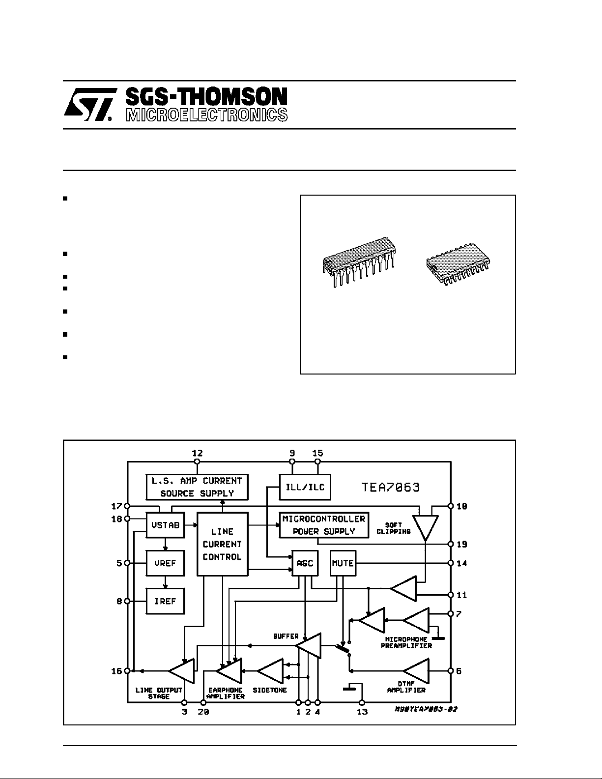
SPEECH CIRCUIT WITH POWER MANAGEMENT
2/4 WIRESINTERFACE WITH
- double antisidetonenetwork
- AC impedance externallyprogrammable
- Rx output dynamic programmable
- AGC attack-disconnectpointsprogrammable
ANTI-CLIPPING/ANTI DISTORTION CIRCUIT
PROGRAMMABLE
DTMF INTERFACE
3.3 VOLTS SUPPLY FOR MICROPROCESSOROR DIALER
EXTRA CURRENT SUPPLY PROGRAMMABLE FOR LOUDSPEAKER
DC CHARACTERISTIC PROGRAMMABLE
FORALL SPECIFICATION
LOW CURRENT OPERATION
TEA7063
PRELIMINARY DATA
DIP20 SO20
ORDERING NUMBERS:
TEA7063FP TEA7063DP
DESCRIPTION
The TEA7063 is designed to meet the different
BLOCK DIAGRAM
worldwide specifications for telephone set in mediumand high range equipments.
January1994
This is advanced information on anew product now in development or undergoing evaluation. Details are subject to change without notice.
1/15
TEA7063
PIN CONNECTION (Top view)
LONG LINE SIDETONE
SHORT LINE SIDETONE
IMPEDANCE
BUFFER OUTPUT
V-REF
DTMF INPUT
MICROPHONE INPUT
I-REF
I START
1
2
3
4
5
6
7
8
9 CURRENT SUPPLY FOR L.S. AMP
19
18
17
16
15
14
13
12
EARPHONE20
MICROCONTROLLER POWER SUPPLY
NOISE FILTER
V-CAPA
V-LINE
I SLOPE
MIC/MIC-EARPHONE MUTE
GND
SQUEEZING THRESHOLD 10 SOFT-CLIPPING FILTER11
D93TL021
ABSOLUTE MAXIMUM RATINGS
Symbol Parameter Value Unit
Max. Current DC (steady) 150 mA
Max. Voltage AC (steady) 7.5 V
Max. Voltage AC + DC (steady) 9 V
Max. Current (20ms) ONE SHOT 1 A
Max. Voltage (20ms) ONE SHOT current < 1A 12 V
P
T
Total Power Dissipation 1 W
tot
Junction Temperature 130 °C
J
MAXIMUMOPERATING CONDITION
Symbol Parameter Value Unit
V
V
I
T
2/15
DC Voltage 7 V
DC
AC Voltage 2.2 Vp
AC
DC Current 110 mA
DC
Temperature Range -20to 70 °C
OP
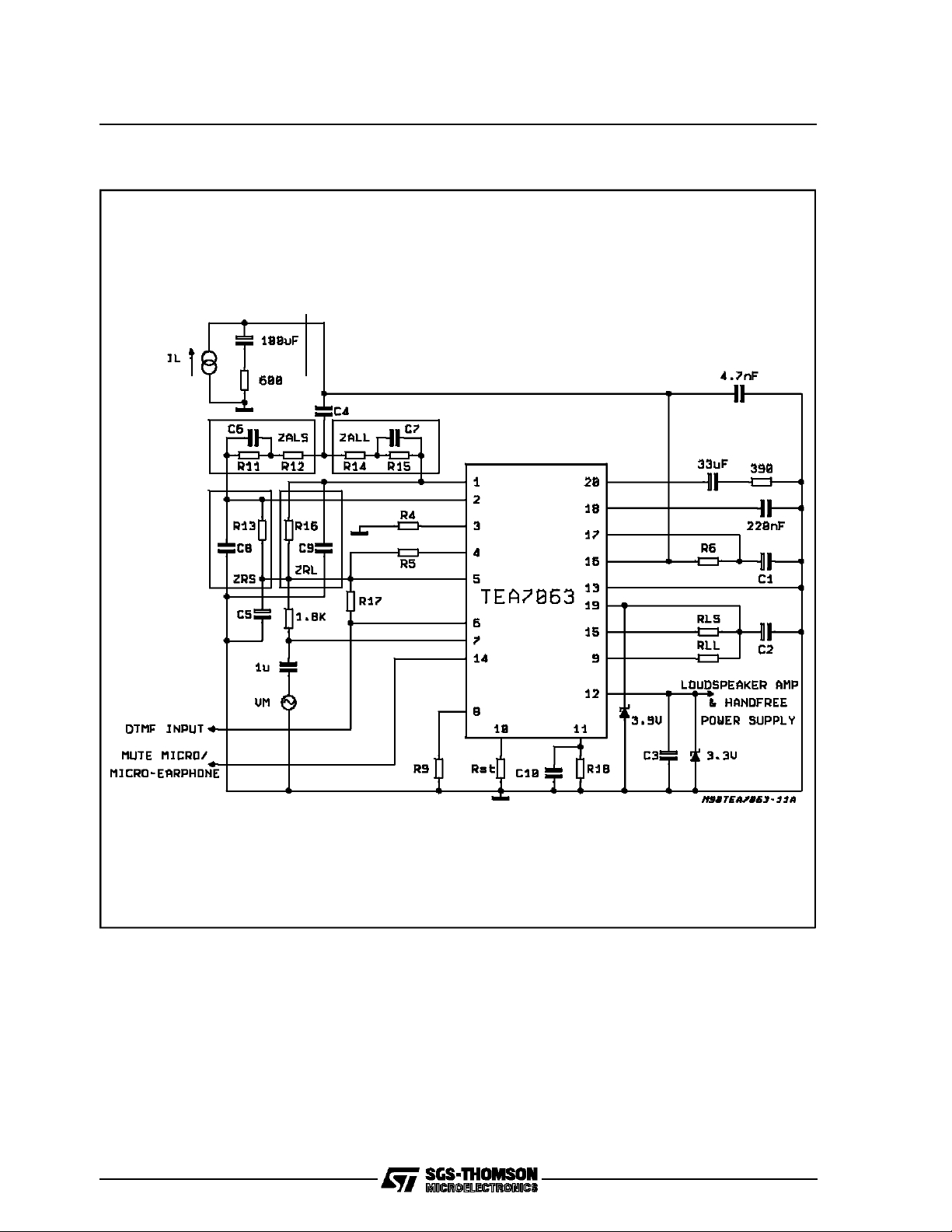
TEST CIRCUIT
TEA7063
R4 = 75
R5 = 5.1K
R6 = 22K
R9 = 100K
R11 = 140K
R12 = 0
R13 = 2.7K
R14 = 0
R15 = 140K
R16 = 2.7K
R17 = 1.8K
R18 = 560K
C1 = 47µF
C2 = 4.7µF
C3 = 47µF
C4 = 470nF
C5 = 100µF
C6 = 47pF
C7 =47pF
C8 =2.2nF
C9 =2.2nF
C10 =150nF
RLL =150K
RLS = 100K
RST= 330K
3/15
TEA7063
ELECTRICAL CHARACTERISTICS (T
=25°C; f = 1KHz; R9 = 100KΩ; unless otherwise specified)
amb
Symbol Parameter Test Condition Min. Typ. Max. Unit
V
Iint Internal Bias Current (pin 17) I
V
I
ref
V
mp
I
cmp
I
spm
I
imp
I
ea
V
mh
V
mb
V
mh
V
mb
I
mleak
G
AGC
G
THD
Z
N
Stabilized Voltage (pin 17) IL= 25mA; R9 = 100KΩ 2.25 2.5 2.75 V
C
= 25mA
L
I
= 25mA; R9 = 180K
L
(V16 - R6*Iint +V
Reference Voltage IL= 25mA 1.05 1.2 1.35 V
ref
Current at V
ref
)
C
120 140
105
-100 +10 µA
160 µA
Stabilized Supply at pin 19 3.1 3.3 3.5 V
Charging Current at Pin19 Pin 17 = GND 0.6 X
I
line
Static Currentat Pin 19 IL= 25mA; R9 = 100KΩ 1.1 1.5 mA
= 25mA; R9 = 180KΩ 0.85 mA
I
L
Internal Consumption 80 110 150 µA
Supply Current for Parallel
Circuits (pin12)
Mute Microphone (pin 14) ON
Mute Earphone (pin 14) ON
IL= 25mA
I
= 75mA
L
OFF
OFF
10
50
12
57
1.6
0.25 0.8
2.7
0.25 2.1
Mute Leakage Current (pin14) V14=5V 20 µA
Tx Gain Long Line IL= 25mA 41.5-742.5-643.5
S
S
f DTMF Gain Pin 14 > 1.6V 41.5 42.5 43.5 dB
m
Tx Distortion IL= 25mA
S
Microphone Impedance 20 KΩ
e
Tx Noise (psometric) IL= 25mA
Tx
V
= -3dBm -GS
mic
V
= -3dBm -GS + 15dB
mic
-74 dBm
-5
3
10
2KΩ at Pins 5-7
R
Tx Attenuation in Mute Mode IL= 25mA
S
60 dB
Pin 14 > 1.6V
G
AGC
THD
N
R
Rx Gain Long Line
r
Line Lenght
r
Rx Distortion IL= 25mA
r
IL= 25mA 29
-7
30
-6
Vro = 500mV
Vro = 630mV
Rx Noise IL= 25mA -74 dBmp
Rx
Rx Attenuationin Mute Mode IL= 25mA
r
50 dB
31
-5
3
10
Pin = 14 > 2.7V
G
Z
G
Antisidetone IL= 25mA 22 dB
as
AC Impedance IL= 25mA 500 650 800 Ω
ac
Confidence Level = V
rs
LINE/VREC
Pin 14 > 2.7V 35.5 38.5 41.5 dB
(in DTMF)
I
ST
Soft Clipping Current Level
Control (pin 10)
V
ST
Control Voltage Range (Pin10) VST=R
IL= 25mA; R9 = 100KΩ
I
= 25mA; R9 = 180KΩ
L
I
x
ST
ST
2.30 2.55
2.80 mA
1.4
01V
µA
mA
mA
mA
V
V
V
V
dB
dB
%
%
psoph
dB
dB
%
%
µA
4/15
TEA7063
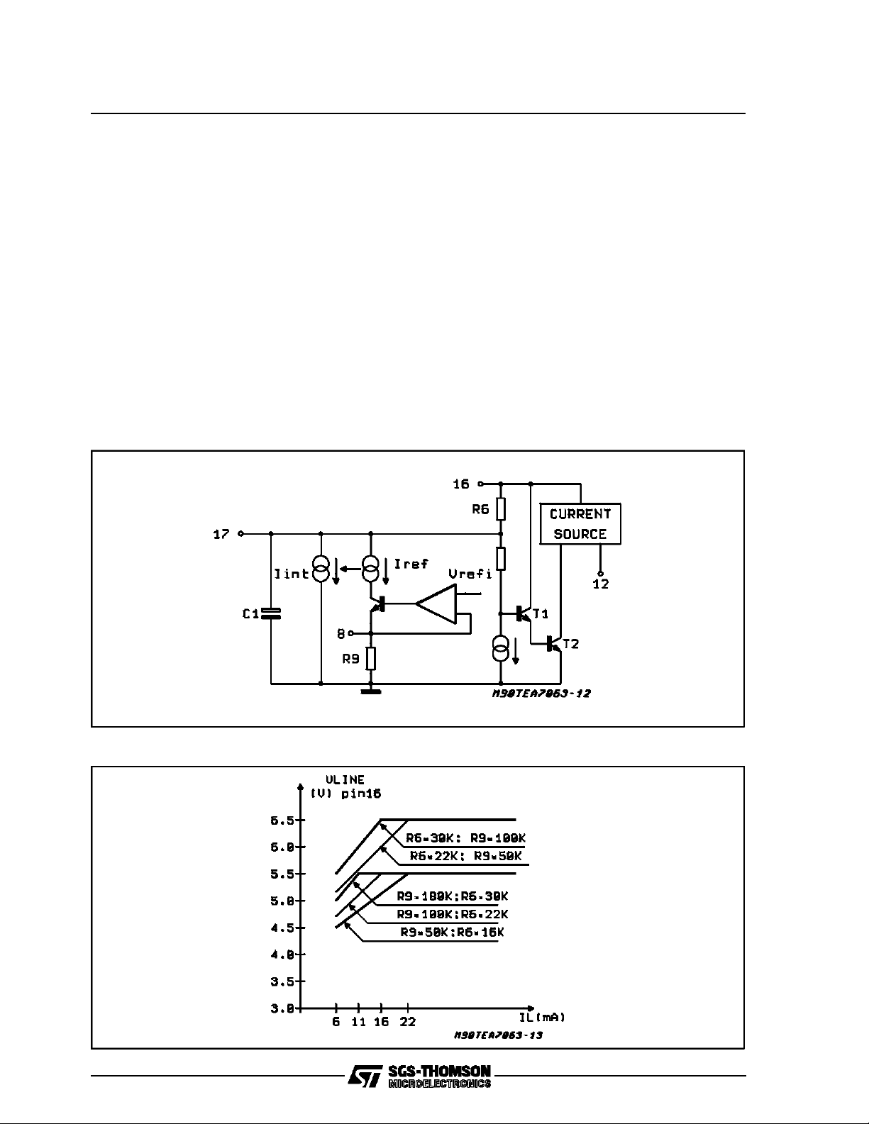
CIRCUITDESCRIPTION
1. DC CHARACTERISTICS
1.1 V
(pin 17)
C
The stabilized voltage VC is connected to Vline
(pin 16) through an internal shunt regulator T1,
T2, which presents to the line a high AC impedance at frequecncies higher than 200Hz. At this
purpose the value of C1 (at pin 17) must be not
lower than 47µF (suggestedvalue is 100µF).
The shunt regulator, T1 and T2, also controls the
extra current source, or power management, at
pin 12 (see also paragraph6).
LINE
(pin 16)
1.2 V
The line voltage (pin 16) is determined by the
value of the external resistor R6 and by the internal current, I
, flowing between VC(pin 17) and
int
Figure1
Ground(seealso paragr.: 1.1):
V
LINE=VC
+R6 xI
int
VCis fixedby design at about2.5V.
I
is reversely related to R9:
int
I
= 8 Volt/R9 + 60µAatIL> 25mA
int
I
= 4 Volt/R9 + 60µAatIL= 6mA
int
where I
depends on ILB(see supply manage-
L
ment)
V
must be externally adjusted (with R6) to
LINE
guarantee both DC and AC characteristic in accordance to the specific standard of the different
adminastrations.
Another adjustment of the DC characteristic is
possible with R9. Increasing the value of R9
causes a decrease of I
duction of the product I
and consequently a re-
int
x R9. (see also Para-
int
graph7)
Figure2
5/15
 Loading...