SGS Thomson Microelectronics TEA6425 Datasheet

.
6 VIDEO INPUTS - 8VIDEO OUTPUTS
.
2 INTERNALSELECTABLEYC ADDERS
.
15MHz BANDWIDTH @ -3dB
.
SELECTABLE 0.5/6.5dB GAIN FOR EACH
OUTPUT
.
HIGH IMPEDANCE SWITCH FOR EACH
OUTPUT(3-stateoperation)
.
PROGRAMMABLE CLAMP MODE ON EACH
INPUT(sync bottom or average value)
.
-60dB CROSSTALK @ 5MHz
.
4 SUB-ADDRESSCAPABILITY
.
I2C BUS CONTROL
DESCRIPTION
Thisdeviceisintendedforswitchingbetweenvideo
and chroma signals such as CVBS,SVHS, baseband CVBS, MAC. Each input clamp mode, each
outputgain, all switchingare controlledthroughthe
2
Cbus.The8 outputscanbesetseparatelyinhigh
I
impedancestate, toenableparallelDC connection
of several devices (up to 4).
TEA6425
VIDEO CELLULAR MATRIX
DIP20
(Plastic Package)
ORDER CODE : TEA6425
SO20L
(Plastic Micropackage)
ORDER CODE : TEA6425D
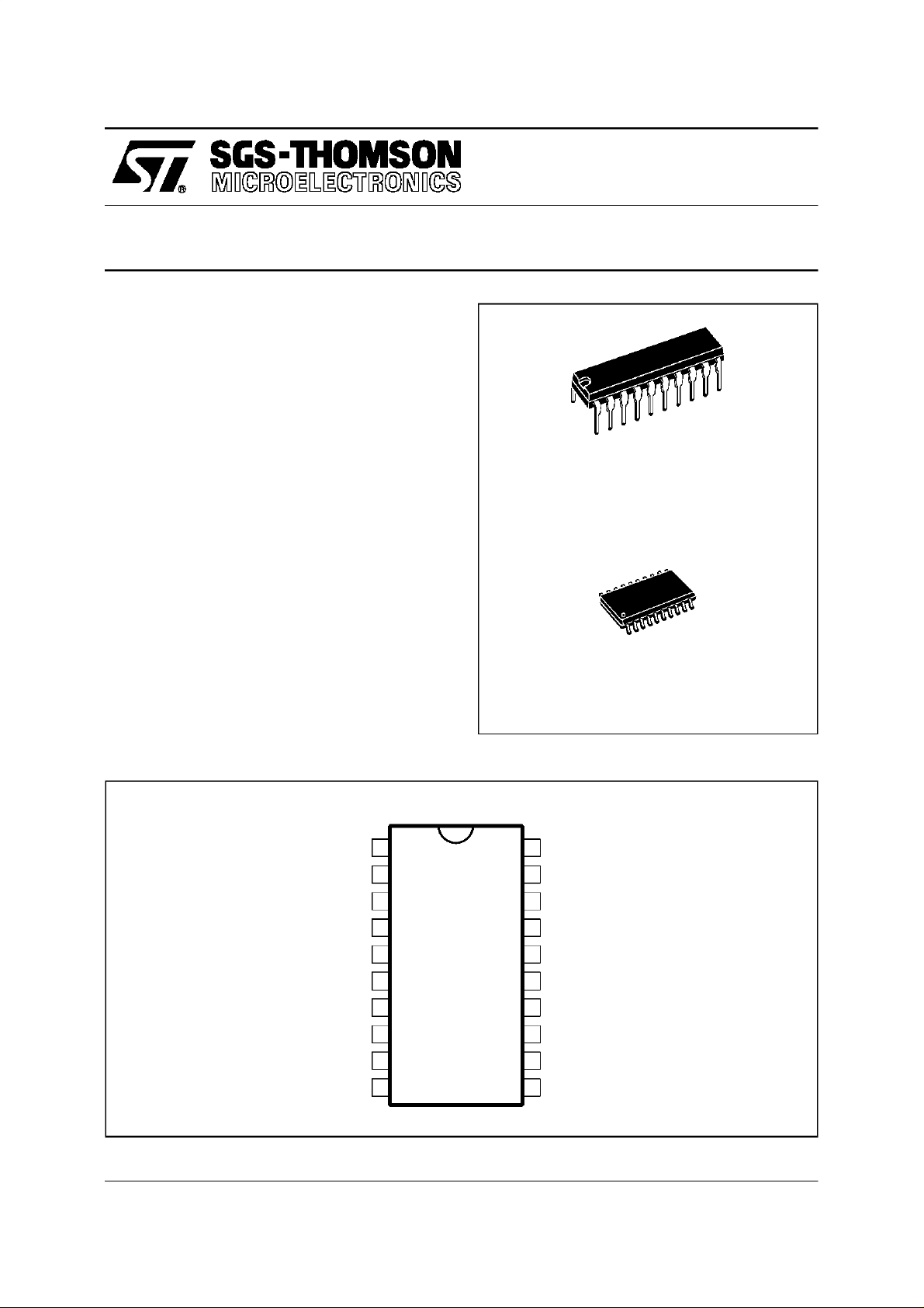
PINCONNECTIONS
May 1996
IN 1
SDA
IN 2
SCL
IN 3
IN 4
SUB
IN 5
V
CCP
IN 6
1
2
3
4
5
6
7
8
9
10
20
19
18
17
16
15
14
13
12
11
V
CC
OUT 1
OUT 2
OUT 3
OUT 4
OUT 5
OUT 6
OUT 7
OUT 8
GND
6425-01.EPS
1/9

TEA6425
BLOCK DIAGRAM
SUB-ADDRESS
INPUTS
SCL
SDA
V
CC1
V
CC2
1
3
5
6
8
10
4
2
7
9
20
TEA6425
PROG.
CLAMP
PROG.
CLAMP
PROG.
CLAMP
PROG.
CLAMP
PROG.
CLAMP
PROG.
CLAMP
I2C
DECODER
6x8
MATRIX
0/6dB0/6dB0/6dB0/6dB0/6dB0/6dB0/6dB0/6
3 S TATE OUTPUTS
11
GND
1312
OUTPUTS
dB
191817161514
6425-02.EPS
CELLULAR MATRICE CONNECTIONS
1st/4addresses
CVBS
or C
PROG.
CLAMP
2
IC
DECODER
6X8
Full MATRIX
IC1
ADDER
6 INPUTS
0dB
6dB
3STATE
OUT
8 OUTPUTS LINES
2nd/4 addresses
2
IC
DECODER
6X8
Full
MATRIX
IC2
6 INPUTS
IC3
IC4
6425-03.EPS
2/9

TEA6425
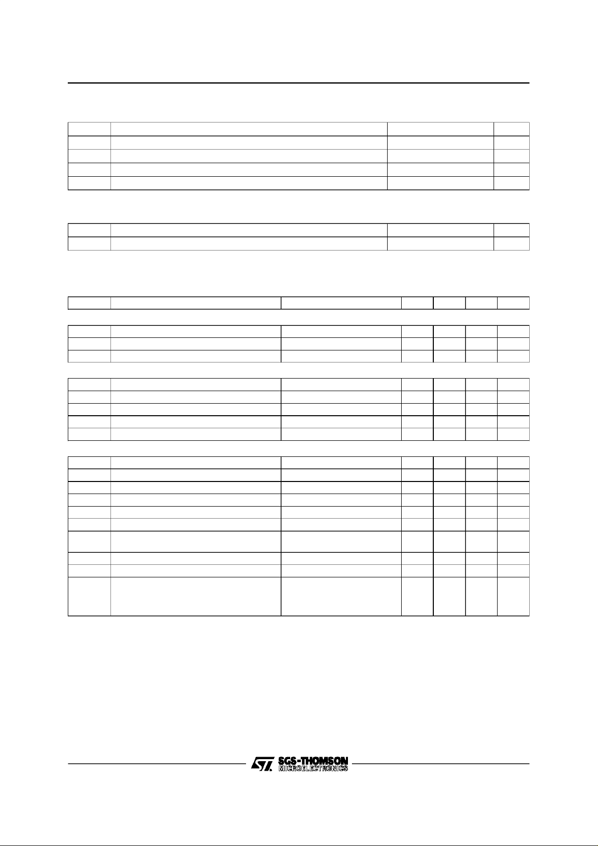
ABSOLUTEMAXIMUMRATINGS
Symbol Parameter Value Unit
V
V
T
oper
T
THERMALDATA
Supply Voltage 12 V
CC
Voltage at Pin i to GND 0, V
I
CC
Operating Ambient Temperature 0, + 70
Storage Temperature -20, + 150
stg
V
o
C
o
C
6425-01.TBL
Symbol Parameter Value Unit
R
th (j-a)
ELECTRICAL CHARACTERISTICS (VCC=8V,T
R
load
Junction-ambient Thermal Resistance Min. 80
=25oC, VIN= 1V, Gain = 6.5dB,C
amb
load
= 4.7kΩ ; Gain condition, clamp and 3-state are controlledby I2C bus, unless otherwisespecified)
=20pF,
o
Symbol Parameter Test Conditions Min. Typ. Max. Unit
SUPPLY
V
I
CC
SupplyVoltage 7.2 8 8.8 V
CC
SupplyCurrent 45 60 mA
RR SupplyVoltage Rejection f = 1kHz 40 46 dB
VIDEO INPUTS (clamping at bottom sync level)
V
V
V
I
clamp
clamp
I
Max. Signal Amplitude Clamp Active 2 V
IN
Clamp Level Clamp Active 1.7 2 2.3 V
InputDC Level Clamp Inactive 2.7 3 3.3 V
DC
Leakage Current 1 input connected to 1 output 2 5 µA
IN
Clamp Current V
- 200mV 0.9 3 mA
clamp
VIDEO OUTPUTS
R
OUT
Z
C
Output Resistance 15 50 Ω
Output ”off” Impedance no load 50 kΩ
HI
C
HI
in 3-state no load 3 pF
OUT
G1 Voltage Gain f = 100kHz 0 0.5 1 dB
G2 Voltage Gain f = 100kHz 6 6.5 7 dB
V
sync
V
Top Level Sync (Y or CVBS) G = 6.5dB, Clamp Active 1 1.25 2 V
Output Mean Level (chroma) G = 0.5dB, Clamp Inactive
bias
G = 6.5dB, Clamp Inactive
2
2.4
3
3.4
3
4
Isolation ”off” State f = 5MHz 60 dB
Crosstalk Attenuation between Channels f = 5MHz 50 60 dB
B Bandwidth C
= 20pF, G = 6.5dB
load
at ± 0.5dB
at ± 1dB
at - 3dB
5
10
21
C/W
PP
V
V
MHz
6425-02.TBL
6425-03.TBL
FUNCTIONAL DESCRIPTION
This device is controlled via the I2C bus. 4 addresses can be selected by a 4-level detector on
Pin 7, thus enabling parallel connection of 4 devices.
2
Viathe I
C bus :
- The input signals can be clampedat their negative peak(top sync).
- The gain factor of the outputs can be selected
between 0.5 and 6.5dB.
- Each of the 6 inputs can be connected to the 8
outputs.
- Each output can individually be set in a high
impedancestate.
Two internal SVHS mixerswill add the selectedY
and C inputs. Twodedicated outputswill have the
option to select this added signalalso.
3/9
 Loading...