

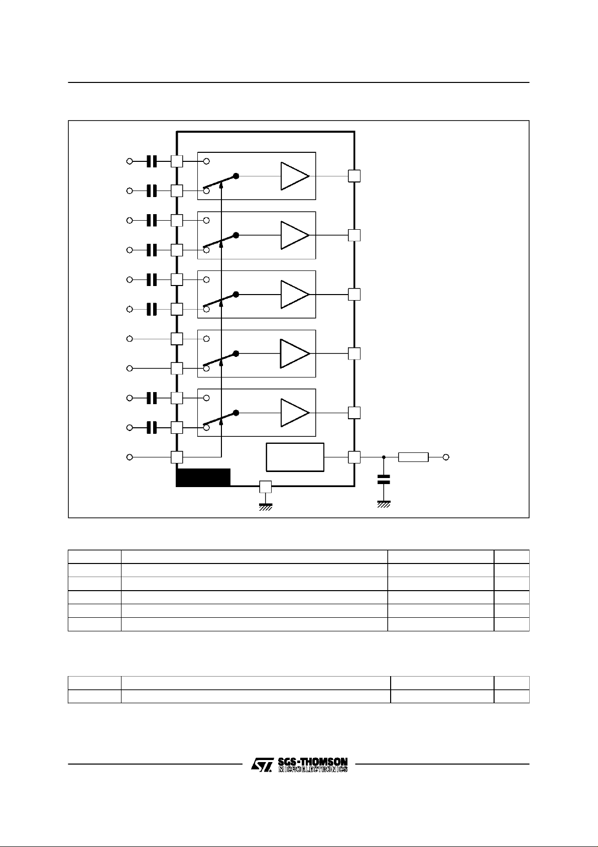
.EACH CHANNEL EXCEPT FAST BLANKING
HAS6dB GAIN
.R, G, B ANDVIDEOSIGNALS ARE CLAMPED
TOTHESAMEREFERENCEVOLTAGEINORDER TO HAVE NO OUTPUT DIFFERENTIAL
VOLTAGEWHENSWITCHING
.ALL INPUTLEVELSCOMPATIBLEWITHNFC
92250ANDEN 50049 NORMS
.30MHzBANDWIDTH FOR R, G,B SIGNALS
.INTERNAL 6.7V SHUNTREGULATORFOR :
LOW IMPEDANCE LOADS,
-
POWERDISSIPATIONLIMITATION
-
.THE FIVE CHANNELS ARE SIMULTANE-
OUSLY SWITCHED BY ONLY ONE SELECT
INPUT
PIN CO NNECTIONS
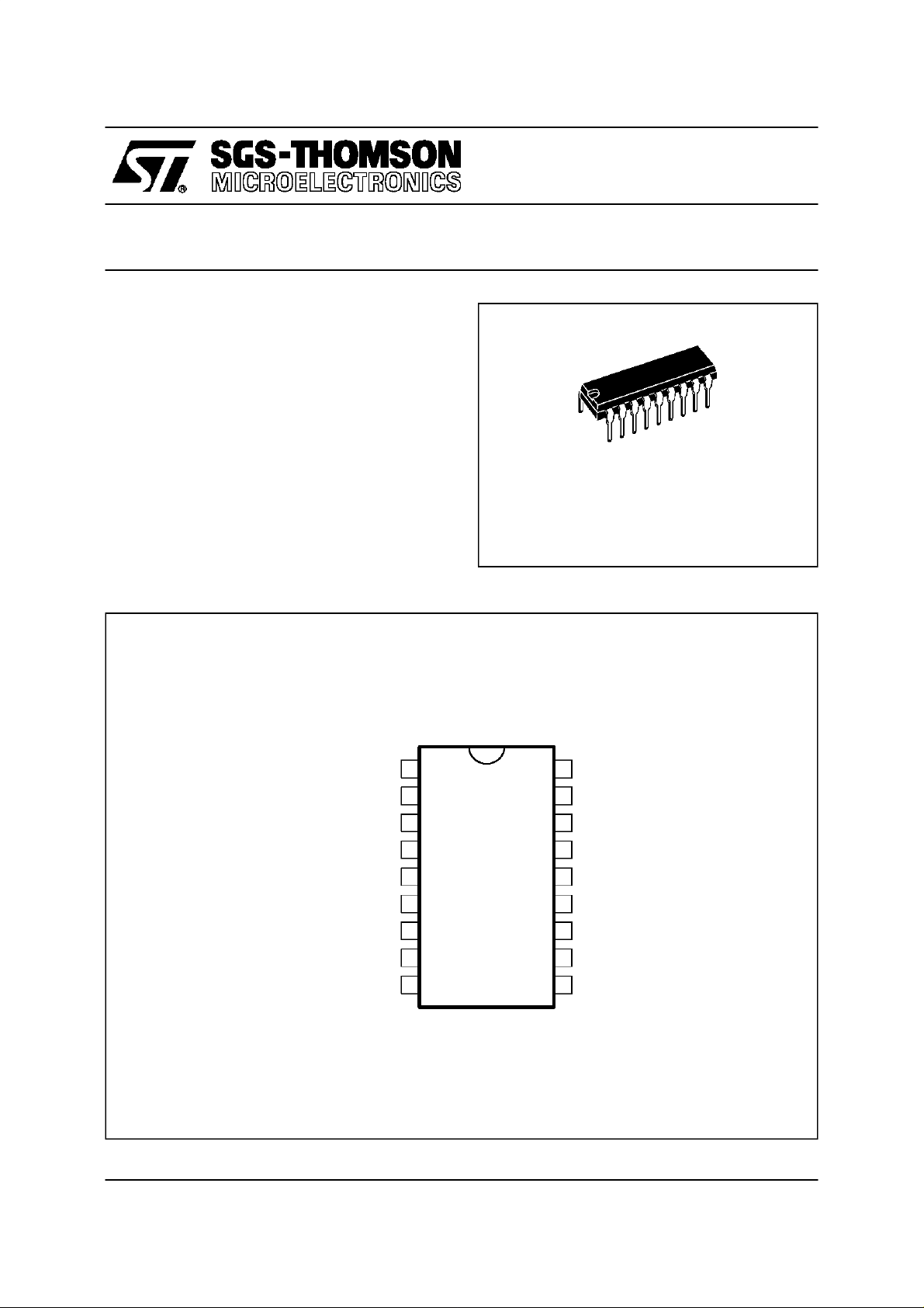
TEA5116
5 CHANNELS VIDEO SWITCH
DIP18
(Plastic Package)
ORDER CODE : TEA5116
May 1996
SYNCHRO SIGNAL INPUT 2
GREEN SIGNAL INPUT 2
”C” SELECT INPUT
GREEN SIGNAL OUTPUT
GROUND
BLUE SIGNAL OUTPUT
SHUNT REGULATOR SUPPLY INPUT
BLUE SIGNAL INPUT 2
1
2
3
4
5
6
7
8
9
18
17
16
15
14
13
12
11
10
GREEN SIGNAL INPUT 1
SYNCHRO SIGNAL INPUT 1
RED SIGNAL INPUT 2
SYNCHRO SIGNAL OUTPUT
RED SIGNAL OUTPUT
FAST BLANKING OUTPUT
RED SIGNAL INPUT 1
FAST BLANKING INPUT 1
BLUE SIGNAL INPUT 1FAST BLANKING INPUT 2
5116-01.EPS
1/8
TEA5116
BLOCK DI AG RAM
R1
R2
G1
G2
B1
B2
FB1
FB2
S1
S2
12
x2
14
R
16
18
x2
4
G
2
10
x2
6
B
8
11
13
FB
9
17
x2
15
S
1
R
V
C
3
SHUNT
REGULATOR
CC
7
PS
V (12V)
PS
TEA5116
5
ABSOLUTE MAXIMUM RATINGS
Symbol Parameter Value Unit
I
CC
V
in
T
oper
T
T
stg
Note : Minimum output l oad is 300 Ω i n case of all outputs l oa ded.
Supply Current (see note) 150 mA
Input Voltage (all inputs) – 0.5 to VCC+ 0.5 V
Operating Temperature Range 0, 70 °C
Junction Temperature – 40, + 150 °C
j
Storage Temperature – 40, + 150 °C
THERMAL DATA
Symbol Parameter Value Unit
Junction-ambient Thermal Resistance 70 °C/W
2/8
R
th (j-a)
5116-02.EPS
5116-01.TBL
5116-02.TBL
TEA5116
ELECTRICAL CHARACTERISTICS
=+25°C, ICC= 120 mA ; Load value = 150 Ω
T
amb
(sequentiallyswitched) (unless otherwise specified, refer to test circuit page 7)
Symbol Parameter Min. Typ. Max. Unit
V
R, G, B Switches (pins 4, 6, 14) (Time Measurement Conditions : ∆ inputs RGB = 0.7 V
C pulse amplitude = 3 V)
V
V
A
A
z
z
t
t
t
t
t
Fast Blanking Switch (pin 13)
(time measurement conditions : FB input pulse amplitude = 2 V, C pulse amplitude = 3V))
V
V
V
V
t
FB1r
t
FB1f
t
FB2r
t
FB2f
t
SFB1r
t
SFB1f
t
SFB2r
t
SFB2f
Internal Shunt Regulator ICC= 120 mA
CC
DC Output Voltage T
C
(no input voltage) T
Max Output Swing Voltage 2 4 V
AC
=90mA
I
CC
= 150 mA
I
CC
junction
junction
=25°C
stabilized
6.3
6.2
6.2
6.7 7.2
7.3
7.3
;
pp
0.9
1.25 V
1.2
B Bandwidth (– 3dB) (input voltage 0.7Vpp) 20 30 MHz
Gain of Each Channel (input voltage 0.7Vpp; f = 1MHz) 5.5 6 6.5 dB
v
Gain Difference between any two R, G, B Channels
dc
(input voltage 0.7V
; f = 1MHz)
pp
0.1 0.5 dB
Input Swing 0.7 V ±
3dB
DC Input Impedance 10 kΩ
ic
Dynamic Output Impedance (input voltage 0.7 Vpp;
oc
f = 1MHz) with R
Crosstalk between any inputs (R1 and R2 or B1 and B2 or G1
and G2) (input voltage 0.7V
Crosstalk between any outputs (input voltage 0.7V
f = 1MHz)
Delay time between R, G, B inputs and RGB outputs. 10 ns
dc
Switching Rise Time between FB1 Input Signal and R, G, B
sr1
Output Signal (input signal on RGB1)
Switching Fall Time between FB1 Input Signal and R, G, B
sf1
Output Signal (input signal on RGB1)
Switching Rise Time between FB2 Input Signal and R, G, B
sr2
Output Signal (input signal on RGB2)
Switching Fall Time between FB2 Input Signal and R, G, B
sf2
Output Signal (input signal on RGB2)
Low Level Input Voltage
IL
High Level Input Voltage
IH
Low Level Output Voltage
OL
High Level Output Voltage T
OH
Dynamic Output Impedance : with R
load
= 300Ω
; f = 1MHz).
pp
45 55 dB
;
pp
40 55 dB
- 0.5
1
=25oC
junction
stabilized
T
junction
= 300Ω 10 Ω
load
1.4
1.5
10 Ω
45 ns
25 ns
55 ns
25 ns
0.4
+0.5
V
CC
+0.5
V
CC
1.7
3.5
1.9
Delay Rise Time between FB1 Input and FB Output 60 110 ns
Delay Fall Time between FB1 Input and FB Output 40 60 ns
Delay Rise Time between FB2 Input and FB Output 60 ns
Delay Fall Time between FB2 input and FB Output 40 ns
Switching Rise Time between C Input and FB Output
75 ns
(input signal on FB1 input)
Switching Fall Time between C Input and FB Output
50 ns
(input signal on FB1 input)
Switching Rise Time between C Input and FB Output
85 ns
(input signal on FB2 input)
Switching Fall Time between C Input and FB Output
50 ns
(input signal on FB2 input)
V
V
V
pp
V
V
V
V
V
5116-03.TBL
3/8

TEA5116
ELECTRICAL CHARACTERISTICS (continued)
Symbol Parameter Min. Typ. Max. Unit
Video (or synchro) Signal Switch (pin 15) - time measurement conditions : (C pulse amplitude = 3V)
V
S
V
as
Z
ic
Z
cc
A
V
B
t
dc
t
sr1
t
sf1
t
sr2
t
sf2
Select Input ”C” (pin 3)
V
IL
V
IH
I
IL
I
IH
DC Output Voltage (no input voltage)
Max Output Swing Voltage
DC Input Impedance
Dynamic Output Impedance (input voltage 1V
load
= 300 Ω
; f = 1MHz)
pp
)
pp
with R
Gain (input voltage 1 V
Bandwidth ( – 3 dB) (input voltage 1 V
T
junction
T
junction
; f = 1MHz)
pp
=25oC
stabilized
2.6
5.5
15
0.9
1.2
10
10
6
20
1.25
6.5
Input Swing 1V ± 3dB
Delay Time between S Input and S Output (∆ input : 0.7VPP)10 ns
Switching rise time between C input signal and S output
45 ns
signal (input signal on S1)
Switching fall time between C input signal and S output
25 ns
signal (input signal on S1)
Switching Rise time between C input signal and S output
55
signal (input signal on S2)
Switching fall time between C input signal and S output
25
signal (input signal on S2)
Low Level Input Voltage
High Level Input Voltage
Low Level Input Current (V
High Level Input Current (V
=1V)
IL
IH
=3V)
– 0.5
2
– 0.6
V
1
+0.5
CC
– 0.1
0.5
V
V
V
pp
kΩ
Ω
dB
MHz
V
V
mA
mA
5116-04.TBL
INPUTS
C
RGBS1
RGBS2
FB1
FB2
OUTPUTS
RGBS
FB
t
dc
4/8
t
FB2r FB2f
tt
t
FB1fFB1r
5116-03.EPS

RGBS2= 0, FB2 = 0
INPUTS
C
RGBS1
FB1
OUTPUTS
RGBS
FB
TEA5116
RGBS1= 0, FB1 = 0
INPUTS
C
RGBS2
FB2
OUTPUTS
RGBS
FB
t
t
SFB1r
t
t
SFB2r
sr1
sr2
t
sf1
t
SFB1f
t
sf2
t
SFB2f
5116-04.EPS
5116-05.EPS
5/8

TEA5116
TEST CI RCUI T
CLOCK
GENERATOR
(TIME
MEASUREMENT)
DYNAMIC
SOURCE
STATIC
SOURCE
STATIC
SOURCE
47nF
1µF
100nF
FB1
11
FB2
9
R1
12
R2
16
G1
18
G2
2
B1
10
B2
8
S1
17
S2
3
C
1
CURRENTSOURCE
120mA
7
V
CC
FB
13
R
14
G
4
B
6
S
15
GND
5
VOLTMETER
TIMEMEASUREMENT
AMPLIFIER
(BANDWIDTH
CROSS-TALK)
150Ω
5116-06.EPS
INPUTS/ O UTPUTS EQ UIV ALENT INTERNAL DIAG RA MS
R, G, B, S inputs (pins 1, 2, 8, 10,12, 16, 17, 18)
Internal
V=3V
V = 6.7V
CCREF
C input (pin 3)
V = 6.7V
CC
10kΩ
3
FB inputs(pins9, 11)
5116-07.EPS
AllOutputs (pins 4, 6, 13, 14, 15)
Pins 9 - 11
V = 6.7V
CC
V = 6.7V
CC
5116-08.EPS
6/8
10kΩ
5116-09.EPS
I = 600µA
5116-10.EPS

INPUTS/ O UTPUTS EQ UIV ALENT INTERNAL DIAG RA MS (continued)
Supply (shunt transistor r egulation system) (Pin 7)
I
CC
TEA5116
7
5
TYPICAL APPL IC ATION DI AGRAM
8 x 100nF
1
7
PERI. TV
PLUG
11
15
20
75Ω
75Ω
75Ω
INTERNALSIGNALS
10kΩ
3.3kΩ
Internal Regulated V
CC
(6.7V typ.)
I
CC
V
REF
max. : 150mA
I typ. : 120mA
CC
Refer to application diagram
+12V
FB1
FB2
R1
R2
G1
G2
B1
B2
S1
S2
C
47Ω 1W
11
12
16
18
10
17
10µF
7
120Ω
13
9
150Ω
14
T
150
E
A
5
2
1
1
6
8
1
3
5
Ω
4
150Ω
6
150Ω 150Ω 150Ω
75Ω
15
R
75Ω
FB
R
G
B
S
TO VIDEO
PROCESSOR
OR TEA5115
5116-11.EPS
75Ω
R values
1) towards TEA5115 : R = 300Ω
75Ω
2) towards video processor : R = 200Ω
•• Above given output load values are minimum values, in case of all output loading.
•• Minimum output load is 150 Ω individually, provided that total supply current is less than 150 mA.
5116-12.EPS
7/8

TEA5116
PACKAGE MECHANI CAL DATA
18 PINS – PLASTIC DIP
Dimensions
Min. Typ. Max. Min. Typ. Max.
Millimeters Inches
a1 0.254 0.010
B 1.39 1.65 0.055 0.065
b 0.46 0.018
b1 0.25 0.010
D 23.24 0.915
E 8.5 0.335
e 2.54 0.100
e3 20.32 0.800
F 7.1 0.280
I 3.93 0.155
L 3.3 0.130
Z 1.27 1.59 0.050 0.063
Information furnished is believed to be accurate and reliable. However, SGS-THOMSON Microelectronics assumes no responsibility for the consequences of use of such information nor for any infringement of patents or other rights of third parties which
may result from its use. No licence is granted by implication or otherwise under any patent or patent rights of SGS-THOMSON
Microelectronics. Specifications mentioned in this publicationare subject to change without notice. This publication supersedes
and replaces all information previously supplied. SGS-THOMSON Microelectronics products are not authorized for use as critical
components in life support devices or systems without express written approval of SGS-THOMSON Microelectronics.
1996 SGS-THOMSON Microelectronics - AllRights Reserved
2
Purchase of I
2
I
C Patent. Rights to use these components in a I2C system, is granted provided that the system conforms to
Australia - Brazil - Canada - China - France - Germany - Hong Kong - Italy- Japan - Korea - Malaysia - Malta - Morocco
The Netherlands - Singapore - Spain - Sweden - Switzerland - Taiwan - Thailand - UnitedKingdom - U.S.A.
C Components of SGS-THOMSON Microelectronics, conveys a license under the Philips
2
the I
C Standard Specifications as defined by Philips.
SGS-THOMSON Microelectronics GROUP OF COMPANIES
PM-DIP18.EPS
DIP18.TBL
8/8
 Loading...