

.25MHzBANDWIDTH
.CROSSTALK: 55dB
.SHORTCIRCUIT TO GROUND OR V
TECTED
CC
PRO-
.ANTISATURATIONGAINCHANGING
.VIDEOSWITCHING
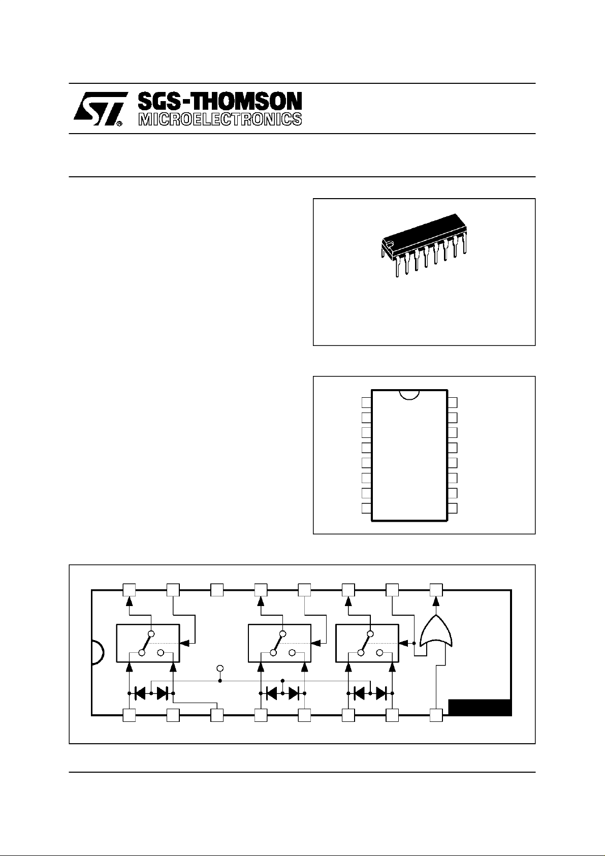
DESCRIP T IO N
This integrated circuit provides RGB switching allowing connectionsbetween peri TV plug, internal
RGBgeneratorand video processorin a TV set.
Theinput signalblacklevel is tied to the same referencevoltageoneachinputinordertohavenodifferentialvoltage when switching two RGB generators.
AnAC outputsignal higherthan 2 Vpp makesgain
goingslowly downto 0dBtoprotecttheTVsetvideo
amplifier from saturation.
Fast blanking outputis a logicial OR between FB1
(Pin8) and FB2 (Pin 10).
TEA5114A
RGB SWITCHINGCIRCUIT
DIP16
(Plastic Package)
ORDER CODE : TEA5114A
PIN CONNECTIONS
FB
R
R
G
G
B
B
INPUT
1
INPUT
2
INPUT
1
INPUT
2
INPUT
1
INPUT
2
INPUT
1
GND
1
2
3
4
5
6
7
8
16
15
14
13
12
11
10
9
R OUTPUT
FB
INPUT
R
V
CC
G OUTPUT
FB
INPUT
G
B OUTPUT
FB2FBB+
FB OUTPUT
INPUT
5114A-01.EPS
BLOCK DI AG RAM
G=2
123
May 1996
10111213
V
14
G=2 G=2
REF
45678
1516
9
OR
TEA5114A
5114A-02.EPS
1/4

TEA5114A
ABSOLUTE MAXIMUM RATINGS
Symbol Parameter Value Unit
V
CC
T
T
stg
Z
L
T
amb
THERMAL DATA
Symbol Parameter Value Unit
R
th(j-a)
ELECTRICAL OPERATING CHARACTERISTICS
=25°C, VCC=12V, ZL(RGB) = 300 Ω
T
amb
Symbol Parameter Min. Typ. Max. Unit
V
CC
I
CC
V
ON
G
RGB
B
RGB
V
GC
V
R
Z
IRGB
Z
ORGB
T
FB
V
IHFB
V
ILFB
Z
IFB
V
OHFB
V
OLFB
Z
OFB
T
dFBRGB
Supply Voltage 18 V
Junction Temperature – 40 to 150 °C
j
Storage Temperature – 40 to 150 °C
Minimum Load Resistor on Each Output VCC=12V
=10V
V
CC
300
150
Operating Ambient Temperature 0 to 70 °C
Junction-ambient Thermal Resistance 80 °C/W
=10V, ZL(RGB) = 150 Ω (unless otherwise specified)
V
CC
Supply Voltage 9 12 13.2 V
Supply Current without Load
=12V
V
CC
Black Level Output Voltage (on pins 11, 13, 16 square wave
20 30 40 mA
1.8 2.5 2.9 V
output signal 1 kHz - 1 Vpp)
=25°C (5mV/°C typical variation)
T
j
Gain of Each Channel Pins 11, 13, 16
F = 1 MHz , V
= 0.5 V
in
pp
Bandwidth (– 3 dB)
=1V
V
O
pp
5 5.5 6 dB
18 22 MHz
Threshold Output Voltage for Gain Changing (– 0.5 dB) 2 V
Video Rejection between Two Inputs R, G or B
F = 1 MHz Sinus V
O
=1V
pp
Input Impedance on Pins 1, 3, 4, 5, 6, 7
=1V
V
O
pp
50 55 dB
10 kΩ
R, G, B Output Impedance on Pins 11, 13, 16 15 Ω
FB rising and falling time on pin 9.
20 ns
1 Vpp Input Voltage Pins 8, 10
FB High Level Input Voltage on Pins 8, 10, 12, 15 1 4 V
FB Low Level Input Voltage on Pins 8, 10, 12, 15 0 0.4 V
Input Impedance on Pins 8, 10, 12, 15 0.7 1 1.3 kΩ
High Level FB Output Voltage (pin 9)
0.8 1 1.2 V
Input 1 V on Pins 8, 10
Low Level FB Output (pin 9)
Input 0 V on Pins 8, 10
FB Output Impedance
Pin 9 High Level
Delay Time between FB Inputs and R, G, B Switching 20 ns
0.3 V
30 Ω
Ω
Ω
5114A-01.TBL
5114A-02.TBL
pp
5114A-03.TBL
2/4

TEST DI AGRAM
V
CC
1µF 100nF
3xZL
6 x 47nF
6x75Ω
OUTPUTS
RGB
B + FB2
1516
91011121314
TEA5114A
12345678
R1 R2 G1 G2 B1 B2
INPUTS
R
G
SWITCHES
CONTROL
FAST
BLANKING
OUTPUT
FAST
BLANKING
INPUT
TEA5114A
5114A-03.EPS
TYPICAL R, G, B SWITCHING APPLICATION
Vcc = 12V
Vcc = 10VZLZL
Typical output
Signal 1Vpp
V
CC
4.7µF
Peritelevisionplug standard input value 1Vpp
300Ω
150Ω
Rout Gout Bout FBout
0.1µF 0.1µF 0.1µF
ZL ZL ZL
1516
G=2
123
6 x 100nF
39Ω
39Ω
R1 G1 B1 FB1
TO VIDEO PROCESSOR
14
G=2 G=2
V
REF
45678
1st GENERATOR
10111213
9
OR
FB2
TEA5114A
B2
2nd
G2
GENERATOR
R2
39Ω
39Ω
5114A-04.EPS
3/4

TEA5114A
PACKAGE MECHANI CAL DATA
16 PINS – PLASTIC DIP
Dimensions
Min. Typ. Max. Min. Typ. Max.
Millimeters Inches
a1 0.51 0.020
B 0.77 1.65 0.030 0.065
b 0.5 0.020
b1 0.25 0.010
D 20 0.787
E 8.5 0.335
e 2.54 0.100
e3 17.78 0.700
F 7.1 0.280
I 5.1 0.201
L 3.3 0.130
Z 1.27 0.050
Information furnished is believed to be accurate and reliable. However, SGS-THOMSON Microelectronics assumes no responsibility for the consequences of use of such information nor for any infringement of patents or other rights of third parties which
may result from its use. No licence is granted by implication or otherwise under any patent or patent rights of SGS-THOMSON
Microelectronics. Specifications mentioned in this publicationare subject to change without notice. This publication supersedes
and replaces all information previously supplied. SGS-THOMSON Microelectronics products are not authorized for use as critical
components in life support devices or systems without express written approval of SGS-THOMSON Microelectronics.
1996 SGS-THOMSON Microelectronics - All Rights Reserved
2
Purchase of I
2
I
C Patent. Rights to use these components in a I2C system, is granted provided that the system conforms to
Australia - Brazil - Canada - China - France - Germany - Hong Kong - Italy- Japan - Korea - Malaysia - Malta - Morocco
The Netherlands - Singapore - Spain - Sweden - Switzerland - Taiwan - Thailand - United Kingdom - U.S.A.
C Components of SGS-THOMSON Microelectronics, conveys a license under the Philips
2
the I
C Standard Specifications as defined by Philips.
SGS-THOMSON Microelectronics GROUP OF COMPANIES
PM-DIP16.EPS
DIP16.TBL
4/4
 Loading...