

SGS Thomson Microelectronics TEA5101A Datasheet

RGB HIGH VOLTAGE VIDEO AMPLIFIER
.
BANDWIDTH : 10MHzTYPICAL
.
RISE ANDFALL TIME : 50nsTYPICAL
.
CRT CATHODES CURRENT OUTPUTS FOR
PARALLEL OR SEQUENTIAL CUT-OFF OR
DRIVEADJUSTMENT
.
FLASHOVERPROTECTION
.
POWER DISSIPATION : 3.5W
.
ESD PROTECTED
TEA5101A
DESCRIPTION
The TEA5101A includes three video amplifiers
desi-gnedwitha high voltageDMOS/bipolar technology. It drives directly the three CRT cathodes.
The deviceisprotectedagainstflashovers. Dueto
its three cathode current outputs, the TEA5101A
canbeused withboth paralleland sequentialsamplingapplications.
PINCONNECTIONS (topview)
15
14
13
12
11
10
9
8
7
6
5
4
3
2
1
MULTIWATT 15
(Plastic Package)
ORDER CODE : TEA5101A
BLUE FEEDBACK
BLUE CATHODE CURRENT
BLUE OUTPUT
GREEN FEEDBACK
GREEN CATHODE CURRENT
GREEN OUTPUT
RED FEEDBACK
GROUND
RED OUTPUT
RED CATHODE CURRENT
V HIGH VOLTAGE
DD
RED INPUT
GREEN INPUT
V LOW VOLTAGE
CC
BLUE INPUT
June 1993
Tab connectedto Pin 8
5101A-01.EPS
1/6
TEA5101A
PIN FUNCTION
N° Function Description
1 Blue Input Input of the ”blue” amplifier. It is a virtual ground with 3.8V bias voltage,
2V
CC
3 Green Input See Pin 1.
4 Red Input See Pin 1.
5V
DD
6 Red Cathode Current Provides the video processor with a copy ofthe DC current flowing into the red
7 Red Output Output driving the red cathode. Pin 7 is internally protected against CRT arc
8 Ground Also connected to the heat sink.
9 Red Feedback Output driving the feedback resistor network for the red amplifier.
10 Green Output See Pin 7.
11 Green Cathode Current See Pin 6.
12 Green Feedback See Pin 9.
13 Blue Output See Pin 7.
14 Blue Cathode Current See Pin 6.
15 Blue Feedback See Pin 9.
15 microamperes input bias current with 14kΩ input resistance.
Low voltage power supply, typically 12V.
Highvoltage power supply, typically 200V.
cathode, for automatic cut-off or gain adjustment. If this control is not used, Pin 6
must be grounded.
discharges by a diode limiting the output voltage to V
DD
.
5101A-01.TBL
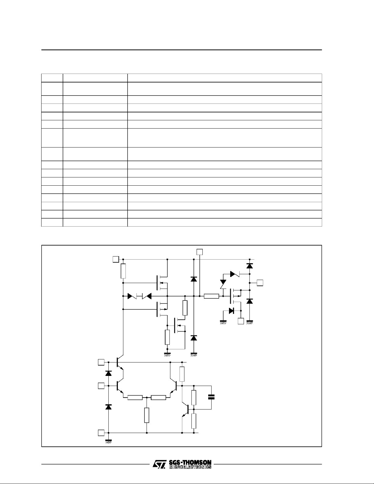
BLOCK DIAGRAM OF EACH CHANNEL
DD
5
40kΩ
2
1
(3, 4)
GND
8
35Ω 35Ω
1kΩ
350Ω
0.8k
(12, 9)15V
13
20k
Ω
Ω
(11, 6)
2.5kΩ
6kΩ
3pF
1.5kΩ
(10, 7)
14
2/6
5101A-02.EPS
 Loading...