

SGS Thomson Microelectronics TEA3717DP Datasheet
.HALF-STEPAND FULL-STEPMODE
.BIPOLARDRIVE OF STEPPERMOTOR FOR
MAXIMUM MOTORPERFORMANCE
.BUILT-IN PROTECTIONDIODES
.WIDERANGE OF CURRENTCONTROL 5 TO
1000mA
.WIDEVOLTAGERANGE10 TO 45 V
.DESIGNED FOR UNSTABILIZED MOTOR
SUPPLYVOLTAGE
.CURRENT LEVELS CAN BE SELECTED IN
STEPSOR VARIEDCONTINUOUSLY
DESCRIP TION
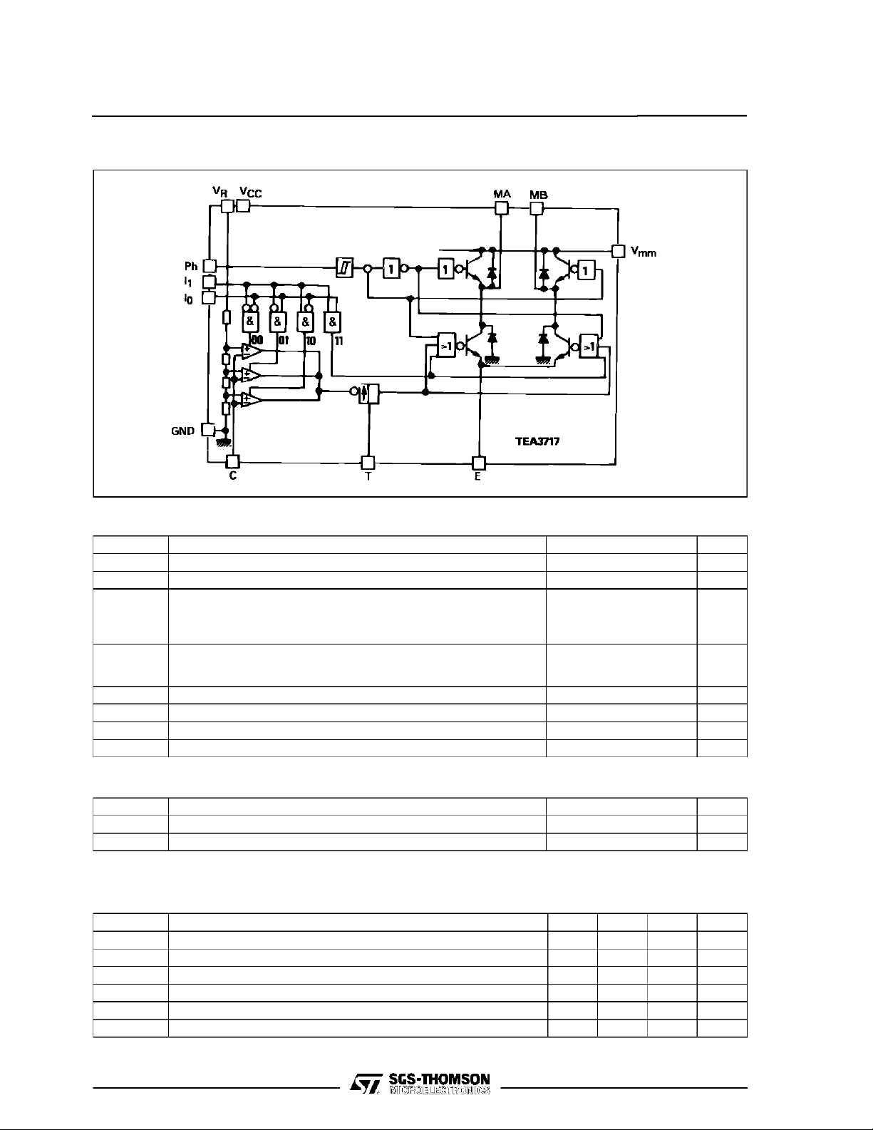
TheTEA3717is a bipolarmonolithicintegratedcircuitintendedto controland drive the current in one
windingof a bipolarsteppermotor.The circuitconsistsof an LS-TTLcompatiblelogic input, a current
sensor,amonostableandanoutputstagewithbuiltinprotectiondiodes.Two TEA3717andafewexternal componentsform a completecontroland drive
unitfor LS-TTLor microprocessor-controlled stepper motorsystems.
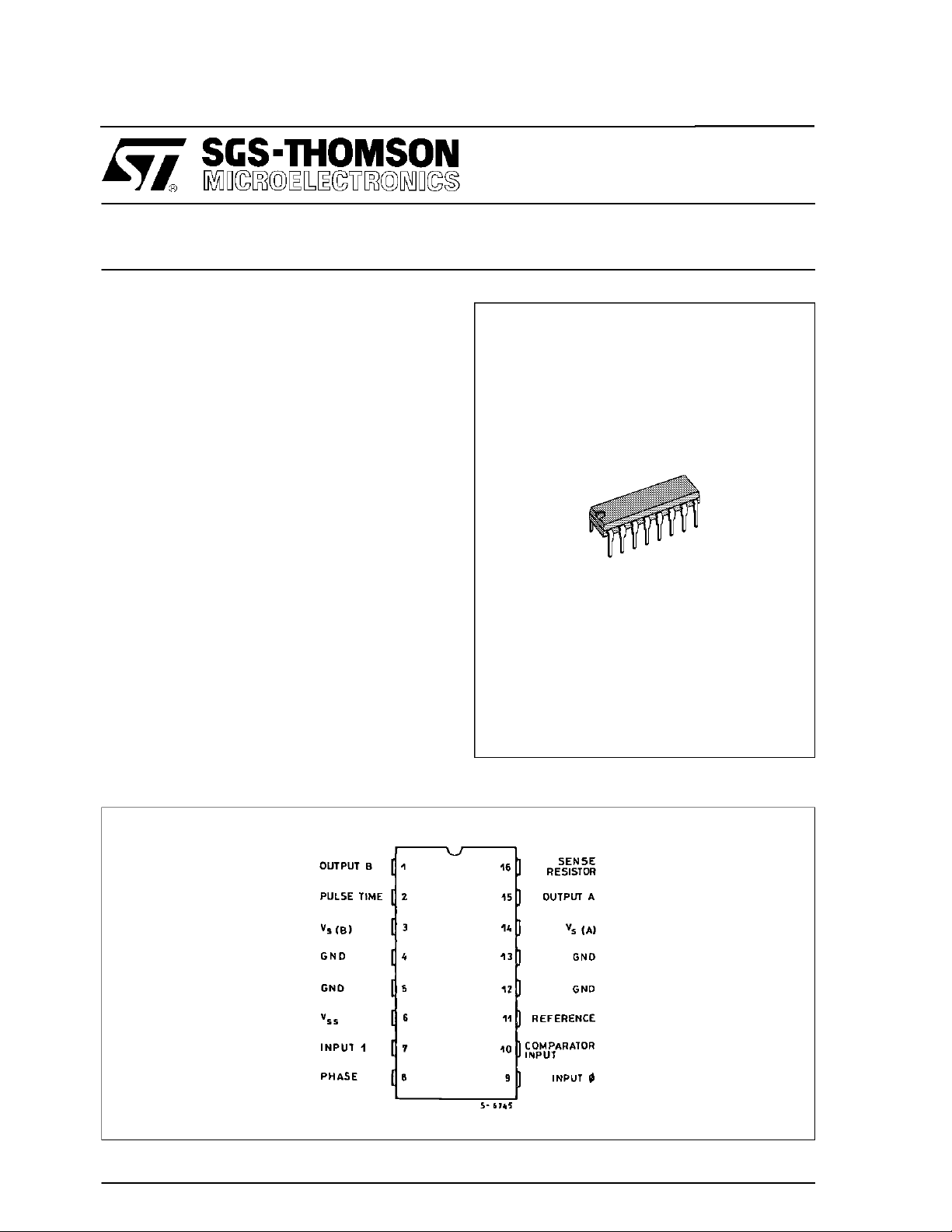
TEA3717
STEPPER MOTOR DRIVER
POWERDIP 1 2 + 2 + 2
ORDER CODE : TEA 3717D P
PIN CONNECTION (top view)
April1993
1/8
TEA3717
SCHEMATIC DIAGRAM
ABSOLUTE MAXIMUM RATINGS
Symbol Parameter Value Unit
V
mm
V
CC
Power Supply Voltage (pins 14, 3) 45 V
Logic Supply Voltage (pin 6) 7 V
Input Voltage
V
in
V
in
V
V
Logic Inputs
Analog Inputs
Reference Input
– 0.5 to 6
V
CC
15
Input Current
I
in
I
in
I
O
T
j
T
stg
T
oper
Logic Inputs
Analog Inputs
–10
–10
Output Current ± 1A
Junction Temperature + 150 °C
Storage Temperature Range – 55 to + 150 °C
Operating Ambiant Temperature Range 0 to + 70 °C
THERMAL DATA
Symbol Parameter Value Unit
R
th (j-c)
R
th (j-a)
*
Solderedon a 35 mm thick 20 cm
Maximum Junction-pins Thermal Resistance 11 °C/W
Maximum Junction-ambient Thermal Resistance 45* °C/W
3
PC board copperarea
RECOMMENDED OPERATING CONDITIONS
Symbol Parameter Min. Typ. Max. Unit
V
CC
V
mm
I
o
T
amb
t
r
t
f
Supply Voltage 4.75 5 5.25 V
Supply Voltage 10 – 40 V
Output Current 0.020 – 0.8 A
Ambient Temperature 0 – 70 °C
Rise Time, Logic Inputs – – 2 µs
Fall Time, Logic Inputs – – 2 µs
V
mA
2/8

TEA3717
ELECTRICAL CHARACTERISTICS
= 5V, ±5%, Vmm= + 10V to + 40V, T
V
CC
Symbol Parameter Min. Typ. Max. Unit
I
V
V
I
I
V
V
V
I
I
V
P
t
Supply Current – – 25 mA
CC
High Level Input Voltage - Logic Inputs 2.0 – – V
IH
Low Level Input Voltage - Logic Inputs – – 0.8 V
IL
High Level Input Current - Logic Input (VI= + 2.4V) – – 20 µA
IH
Low Level Input Current - Logic Inputs (VI= + 0.4V) – 0.4 – – mA
IL
Comparator Threshold Voltage (VR= + 5.0V), I0=0,I1=0
CH
CM
CL
Comparator Input Current – 20 – 20 µA
CO
Output Leakage Current (I0=1,I1=1)
off
Total Saturation Voltage Drop (Io= 500mA) – – 4.0 V
sat
Total Power Dissipation
tot
Cut off Time (seefigure 1 and 2, Vmm= + 10V, ton≥ 5µs) 25 30 35 µs
off
Turn off Delay (see figure 1 and 2, T
t
d
=+25°C
T
amb
=+70°C, VS= 40V, VSS=5V
T
amb
= 500mA, fs= 30kHz
I
o
= 800mA, fs= 30kHz
I
o
=0oCto+70oC (unlessotherwisespecified)
amb
=1,I1=0
I
0
=0,I1=1
I
0
230
65
–
–
–
–
=+25°C, dVC/dt ≥ 50mV/µs) – 1.6 µs
amb
390
420
250
80
–
100
1.8
3.7
440
270
100
200
90
2.3
–
mV
µA
W
Figure2.Figure 1 (seenote)
3/8
 Loading...