

SWITCH MODE POWER SUPPLY PRIMARYCIRCUIT
.
POSITIVE AND NEGATIVE OUTPUT CURRENTUP TO 1.2AAND – 1.7A
.
A TWO LEVEL COLLECTOR CURRENT LIMITATION
.
COMPLETETURN OFF AFTERLONG DURATIONOVERLOADS
.
UNDERANDOVER VOLTAGELOCK-OUT
.
SOFT START BY PROGRESSIVE CURRENT
LIMITATION
.
DOUBLEPULSESUPPRESSION
.
BURST MODE OPERATION UNDER STANDBY CONDITIONS
DESCRIPTION
In amasterslave architecture,theTEA2164control
IC achieves the slave function.Primarilydesigned
for TV receivers and monitors applications, this
circuitprovidesaneasy synchronizationand smart
solutionfor low powerstand by operation.
Located at the primary side the TEA2164 Control
IC ensures:
- the powersupply start-up
- the power supply control under stand-by conditions
- the process of the regulation signalssent by the
mastercircuitlocated at the secondaryside
- directbasedriveofthebipolarswitchingtransistor
- the protection of the transistor and the power
supplyunder abnormalconditions.
For more details, refer toapplicationnote AN409.
TEA2164
POWERDIP16
(Plastic Package)
ORDER CODE : TEA2164
PINCONNECTIONS
LONG CAPACITOR OVERLOAD CAPACITOR
OSCILLATOR TIMING RESISTOR
OSCILLATOR TIMING CAPACITOR
December 1992
GROUND
I COPY
SUBSTRATE
SUBSTRATE
PULSE INPUT
V SUPPLY VOLTAGE
1
2
3
4
5
6
7
8
16
CC
OUTPUT STAGE POSITIVE SUPPLY VOLTAGE
15
OUTPUT (BASE CURRENT)
14
SUBSTRATE
13
SUBSTRATE
12
I SENSE
11
C (max.)
LOW FREQUENCY OSCILLATOR CAPACITOR
10
FEEDBACK INPUT IS BURST MODE
9
2164-01.EPS
1/15
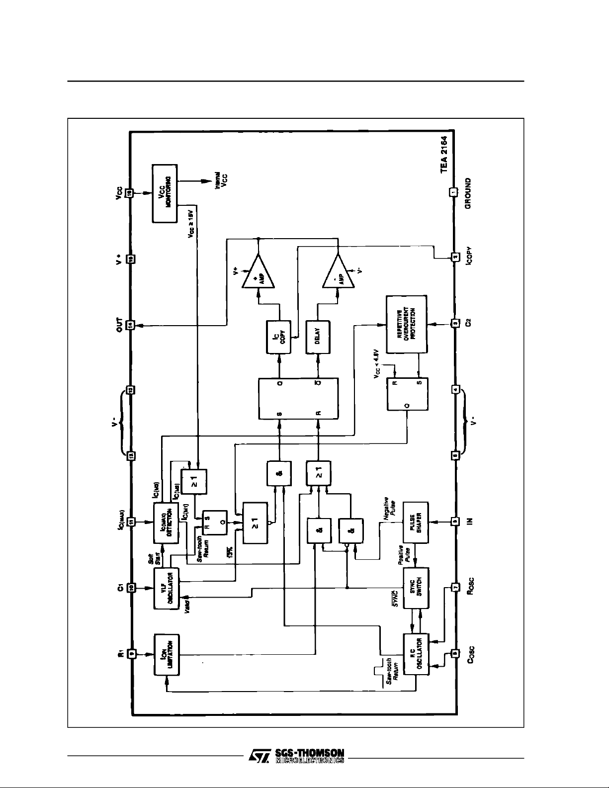
TEA2164
BLOCK DIAGRAM
2/15
2164-02.EPS
TEA2164
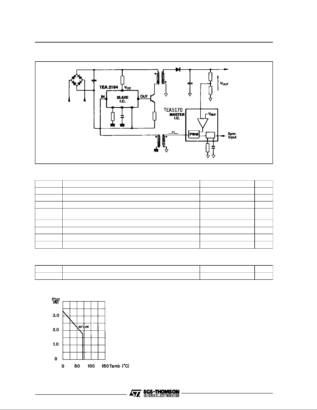
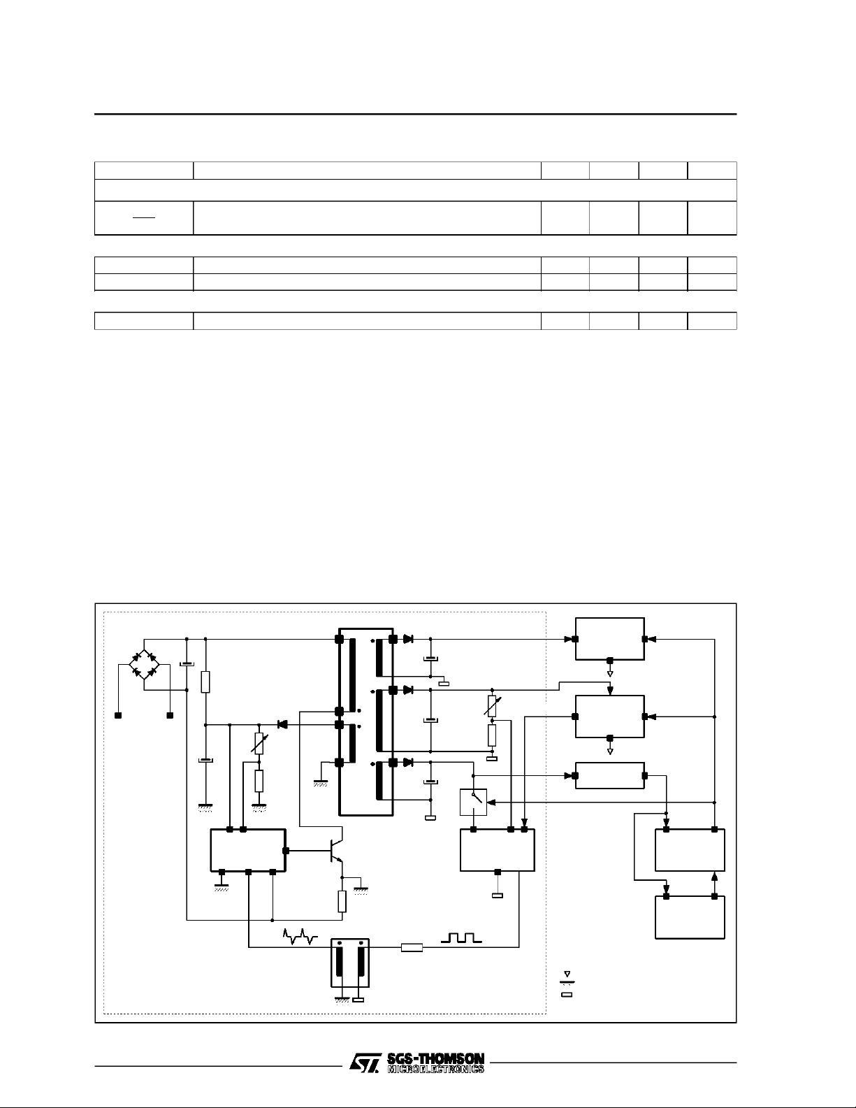
Figure 1 : SimplifiedApplication Diagram
ABSOLUTEMAXIMUM RATINGS
Symbol Parameter Value Unit
V
CC
V+ Positive Power Supply of the Output Stage V15-V1 18 V
V– Negative Power Supply V4, 5, 12, 13-V1 – 5 V
-V–
V
CC
V+ - V–
I
out+
I
out–
T
T
stag
Positive Power Supply V16-V1 18 V
Total Power Supply V16-V4, 5, 12, 13 or V15-V4, 5, 12, 13 20 V
Positive Output Current 1.5 A
Negative Output Current 2 A
Operating Junction Temperature 150 °
j
Storage Temperature Range –40, + 150 °
2164-03.EPS
C
C
2164-01.TBL
THERMALDATA
Symbol Parameter Value Unit
R
th(j-c)
Junction Case Thermal Resistance 11 °
MAXIMUMPOWER DISSIPATION
2164-04.EPS
C/W
3/15
2164-02.TBL
TEA2164
RECOMMANDED OPERATING CONDITIONS
Symbol Parameter Min. Typ. Max. Unit
V
CC
V– Negative Power Supply (absolute value) (note 1) 0 5 V
V
– V– Total Power Supply 18 V
CC
I
out+
I
out–
Fsw Switching Frequency 50 khz
Ro Oscillator Resistor Range 30 150
Co Oscillator Capacitor Range 470 2700 pF
C1 StartingOscillator Capacitor Range 0.1 4.7 µ
C2 Repetitive Overload Protection Capacitor 1 22
V
in
T
oper
Positive Power Supply 10 14 V
Positive Output Current 1.2 A
Negative Output Current 1.7 A
Input Pulses Amplitude (peak) (derivated pulses - time constant = 1 µs)
0.5 1 V
Operating Ambiant Temperature – 20 70 °
-
V
CC
I>0
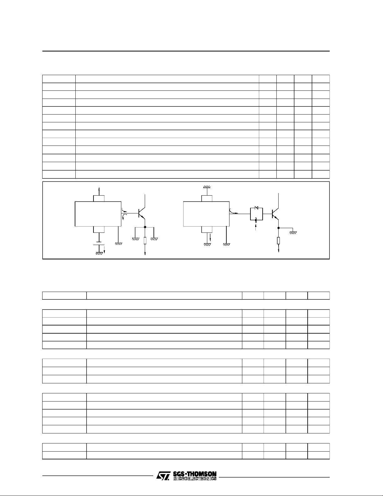
14
<0
B
<0
I
B
1312
TEA2164
5
4
I
I
B
I
14
1
capacitive
<0
B
coupling
12 13
TEA2164
45 1
-
V
CC
I
B
kΩ
µF
F
C
2164-03.TBL
2164-05.EPS
ELECTRICAL OPERATING CHARACTERISTICS
=25oC, VCC=10V, V
T
amb
= 0V, potentialsreferencedto ground (Pin 1)
CC-
(unlessotherwise specified)
Symbol Parameter Min. Typ. Max. Unit
POWER SUPPLY
(start) Starting Voltage (VCCincreasing) 8 9 9.6 V
V
CC
V
(stop) Stopping Voltage (VCCdecreasing) 5 6.2 7.4 V
CC
∆V
CC
V
ccmax
I
ccstart
CURRENT LIMITATION AND PROTECTION (pin 11)
VCM1 Pulse by Pulse Current Limitation Threshold 720 840 970 mV
VCM2 Current Monitoring 2nd Threshold 1200 1350 1500 mV
∆VCM ∆VCM = VCM2 – VCM1
REPETITIVEOVERCURRENT PROTECTION
VCM3 Repetitive OvercurrentThreshold (pin 11) 700 900 1100 mV
VCM3-VCM1 (VCM3-VCM1) – 20 50 130 mV
VC2 Lock-out Voltage on Pin 3 2.4 3 3.6 V
I3 disch Capacitor C2 Discharge Current (synchronizedmode) 10 20 30 µ
I3 ch. Capacitor C2 Charge Current 50 80 110 µ
OSCILLATOR, MAX DUTY CYCLE, SYNCHRONIZATION
T
o
T
on(max)
Hysteresis (VCCstart – VCCstop) 2 2.8 3.5 V
Overvoltage Lock-out 14.8 15.5 16.2 V
Starting Positive Supply Current 0.5 0.8 1.5 mA
300 500 700 mV
Oscillator Initial Accuracy RT = 50 K, CT = 1 nF 19.3 21 22.7
Maximum Duty Cycle (T
= 1.05 To)607085%
syn
A
A
µs
2164-04.TBL
4/15
ELECTRICAL OPERATINGCHARACTERISTICS (continued)
Symbol Parameter Min. Typ. Max. Unit
OSCILLATOR, MAX DUTY CYCLE, SYNCHRONIZATION (continued)
T
syn
T
O
OUTPUT STAGE
I
14/I2
I
BON
VERY LOW FREQUENCY OSCILLATOR
Synchronization Window 1.0 1.5
IcCopy CurrentGain 1000
Base Current Starting Pulse 300 mA
Burst Duty Cycle 13 %
TEA2164
2164-05.TBL
I. FIELD OF APPLICATION
The TEA2164 control circuit has been designed
primarily for discontinuousmode flybackbuilt with
a master-slave architecture, whatever the field of
application.
Butdue to its capabilityto synchronizethe transistor switching-off with an external signal (line flyback)and dueto an adaptedburst-modeoperation
for a low power stand-by operation, the TEA2164
offers a smart solution for monitors and TV sets
applications.
Powersupply main features:
- maximumoutput power 140W (transistorforced
gain : 3.5)
Figure 2 : MasterSlave PowerSupplyArchitecture
R
MAINS
INPUT
P
C
V
CC
2
- stand-bymode output power (1W ≤ Psb ≤ 6W ;
efficiency > 50%)
- operatingfrequencyup to 50kHz
- power-switch : bipolar transistor
Adaptedmaster-circuit :
Monitorapplication → TEA5170
Standard TV application → TEA2028B
TEA2029C
TEA2128
TEA5170
Digital TV application → TEA5170
(TEA2028B,TEA2029Cand TEA2128 are deflec-
tion processorswith built-in PWM generator).
Muting
Control
Remote
Stand-by
Remote
Stand-by
P
1
Synchronization
AUDIO
OUTPUT
STAGE
SCANNING
DEVICE
VOLTAGE
REGULATOR
TEA2164
P : Output voltage adjustement in normal mode
1
P : Output voltage adjustement in stand-by
2
TEA5170
PWM
µP
V
CC
INFRA-RED
RECEIVER
Small signal primary ground
Power primary ground
Secondary ground (isolated from mains)
2164-06.EPS
5/15

TEA2164
II. GENERALDESCRIPTION
In a masterslave architecture,the TEA2164 Control IC, located at the primary side of an off line
powersupplyachievestheslavefunction;whereas
Figure 3 : SystemDescription Waveforms
the mastercircuitis locatedat the secondaryside.
The linkbetweenboth circuitsis realizedbyasmall
pulse transformer(Figure 3).
6/15
2164-07.EPS

TEA2164
In the operation of the master-slave architecture,
four majors casesmustbe considered :
- normaloperating
- stand-bymode
- powersupplystart-up
- abnormalconditions : off load,short circuit,...
II.1.Normal Operating (master slave mode)
In this configuration,themastercircuit generatesa
pulsewidthmodulatedsignalissuedfromthemonitoring of the output voltage which needs the best
accuracy(inTVapplications:thehorizontaldeflectionstagesupplyvoltage).Themastercircuitpower
supplycan be suppliedby another output.
The PWM signalare sent towards the primary side
through small differentiating transformer. For the
TEA2164 positive pulses are transistor switchingon commands; and negative pulsesare transistor
switching-offcommands(Figure 4). In this configuration,only by synchronizingthe masteroscillator,
the switchingtransistor may be synchronizedwith
an externalsignal.
II.2.Stand-byMode
In this configuration the master circuit no longer
Figure 4 : MasterSlave Mode Waveforms
sends PWM signals, the structure is not synchronized ; and the TEA2164 operates in burst mode.
The averagepower consumptionat the secondary
side may be very low 1W ≤ P ≤ 6W (as it is
consumedin TV set during stand by).
By action on the maximum duty cycle control, a
primary loop maintains a semi-regulation of the
outputvoltages.Voltageonfeed-backisappliedon
Pin 9.
Burstperiodis externallyprogrammedbycapacitor
C1.
II.3.Power Supply Start-up
After the mains have been switched-on, the V
CC
storage capacitor of the TEA2164 is charged
through a high value resistor connected to the
rectifiedhigh voltage.When VccreachesV
CC
start
threshold(9V typ), theTEA2164startsoperatingin
burst mode. Sinceavailable outputpower islow in
burst mode the output power consumption must
remain low before complete setting-up of output
voltage. In TV application it can be achieved by
maintaining the TV in stand-by mode duringstartup (Figure 6).
SLAVE
CIRCUIT
Synchro.
MASTER
CIRCUIT
Sync.
Pulses
PWM
Signal
Pulse
Input
Base
Current
2164-08.EPS
7/15

TEA2164
Figure 5 : BurstMode Waveforms
Figure 6 : PowerSupplyStart-up
2164-09.EPS
Tch ≈ 1s (typ)
T1 ≈ 0.3s (typ)
T
start-up
= Tch + T1
T1 :necessary time for voltagesetting-up
d) Abnormalconditions: safetyfunctions
OvervoltageProtection
When V
exceeds VCCmax, an internal flip-flop
CC
stops output conduction signals. The circuit will
start again after the capacitor C1 discharge ; it
means : after loss of synchronizationor after Vcc
stopcrossing (Figure7).
In flyback converters, this function protects the
powersupply against outputvoltagerunaway.
Under Voltage Lock-out
The TEA2164 controlcircuitstops operatingwhen
goes under VCCstop.
V
CC
8/15
Power Limitation,Current Protection, Long
Duration OverloadProtection
- Output power limitation : by a pulse by pulse
collectorcurrentlimitation the TEA2164 limits the
maximum output power. V
isthe correspond-
CM1
ing voltagethreshold,its detection is memorized
up to the next period.
- Currentprotection(transistorprotection)
Under particular conditions a hard overload or
short circuit may induce a fluxrunawayin spiteof
the currentlimitation (V
CM1
).
The TEA2164 control circuit features a second
current protection, V
. When this thresholdis
CM2
reached an internal flip-flop memorizes it and
2164-10.EPS

TEA2164
output conduction signals are inhibited. The circuitwill sendbasedrivesagainaftercapacitorC1
discharge(Figure7).
- Longdurationoverloadprotection : (Figure 8)
An overload is detectedwhen thesense-voltage
on Pin 11 reachesV
before a negativepulse
CM3
hasbeenappliedto Pin 6. In thiscasethe capacitor C2 (connectedto Pin3) is charged with I
up to theendof the period and discharged with I
disch until a next V
detector. By this way in
CM3
ch
3
3
case of long duration overload, the capacitor
Figure 7 : OvervoltagesLock-out
Figure 8 : LongDuration Overload Monitoring Circuit
keeps charging at each period and its voltage
encreasesgradually. When the voltage on Pin3
exceeds V
, the TEA2164 control circuit stops
C2
sending base drives and memorizes this event.
No restart is allowed as long as V
than V
andVCChigherthan 4.8V.
C2
pin 3
is higher
* Remark:
- The harder is the overload the faster is the protection
- The capacitorkeeps chargingbetween two burst
after V
CM2
detection.
2164-11.EPS
Figure 9 : LongDuration Overload Detection
2164-11.EPS
2164-13.EPS
9/15

TEA2164
Figure 10 : RepetitiveOver-current Protection
III. SWITCHINGOSCILLATOR AND SYNCHRONIZATION
III.1. Switchingoscillator
Whenthe TEA2164controlcircuitoperatesin burst
mode, the switching frequencyis fixed by the free
frequency oscillator. The period is determined by
two external componentsC
andRO.
O
III.2. Synchronization
Whenthe master-circuitstarts to send pulsesboth
Figure 11 : Free Frequency Running
oscillators are not synchonuous. In order to avoid
any erratic conductionof the power transistor,the
firstsynchronizationpulse will arrive simultanously
with thesawtoothreturn of the TEA2164oscillator.
Toget synchronizationthe free frequency must be
higher than the synchronizationfrequency.
T
O<Tsync.
< 1.50 T
2164-14.EPS
O
Figure 12 : SynchronizationPulse Shaperand Synchronization
10/15
2164-15.EPS
2164-16.EPS

Operationafter synchronization
TEA2164
(1) NORMAL OPERATION
∆T :synchronization window
Operationafter synchronization
(3) ERRATIC POSITIVE PULSES
P1 and P2 are masked due to the synchronization window
Cases (2) (3) (4) donot occur in normal operating.
IV - MAXIMUM DUTY CYCLE LIMITATION
Burstmode :Themaximum dutycycleiscontrolled
by the voltage on Pin 9 (Figure13).
Synchronizedmode : Normallythe maximum duty
cycle is set by the master circuit. Oowever the
maximum conducting time will never exceed the
value given by the comparison of the oscillator
wave-formwith the 2.5Vinternal threshold.
V - OUTPUTSTAGE
TEA2164output stage has beendesignedto drive
switchingbipolar transistor.
- Eachbase drive beginswitha positivepulseI
BON
(2) NEGATIVE PULSE MISSING
Transistor turn-off is ensured by VCM1 current limitation crossing or byan internaltON (max.) limitation set by a 2.5V threshold
(4) Fsynchro < 0.65 Fo
Signal S1 triggers burst oscillator capacitor discharge.
The TEA2164 restarts in burst-mode
thatrealizesan efficienttransistorturn-on.
- After the starting pulse I
, the base currentis
BON
proportionalto the collector current. The current
gain is easily fixed by a resistorR (Figure14).
- A fast and safetransistor turn-off is realized by a
fastpositivebase currentcut-off and by applying
a negativebase drive which draws stored carriers.A typical 0.7sdelaypreventsfromcross-conductionof positiveand negative outputstages.
Remark : In order to reducepower dissipationon
the positiveoutput stage with the lowgain transistors,forhighbasecurrentsthepositiveoutputstage
operatesin saturated mode (Figure 15). This can
be achievedby using a resistorbetween V
CC
and
V+.
2164-17.EPS / 2164-18.EPS
2164-19.EPS
11/15

TEA2164
Figure 13 : MaximumDuty Cycle Limitation
Figure 14 : OutputStage Architectureand Base Drive
2164-20.EPS
V
4-5-12-13
V
I
14
B
R
S
R
B
I
C
The energy of the starting burst must be high
enough to ensure start-up, then the capacitor C1
must be higher in these applicationsthan on TV
application(typ. : 1µF).
16 15
V
CC
CURRENT
MIRROR
Virtual
Ground
2
I
COPY
VI - MONITOR APPLICATIONS
In most of monitor applications, the power supply
must start-up under full load conditions and the
stand-by mode is no longer useful.
Figure 15 : PowerSupply Start-up andNormal Operation
I
Cmax
I
I
B
C
I
BON
I
C
≅ GF
I
B
I
C
GF = =
I
B
R
S
R
B
1000 x R
t
t
V
CM1
=
I
Cmax
S
2164-21.EPS
12/15
2164-22.EPS

COMPLETE APPLICATION DIAGRAM(SMPS + DEFLECTION) (with stand-by function)
+24V
+200V
Ω
Frame
Adjust
60
ESM
4.7µF
BA157
740
Ω
220
220Ω
Ω
220
100Ω BA159
4
18
1N4444
390
Amplitude
33Ω
820Ω
6
+24V
Ω 4.7Ω
220
220Ω
6.8kΩ
3.3kΩ
3.3kΩ
6.8kΩ
100nF
Ω
1k
820Ω
2.7MΩ
3
1
2
200V
Ω1kΩ
82k
Adjust
FramePhase
E/W
470nF
Ω
220k
Ω
2.2k
5
10kΩ
28
11
SUPER
SANDCASTLE
LINE
4.7nF
100nF
TEA2029C
220nF
100nF
VIDEO
15 27 26 25 12
7
22
19
1.5nF
220Ω
15nF4.7
3.9kΩ
503
kHz
F
µ
F
µ
10
24
20
1N4148
MUTEOUT
8.2kΩ
330Ω
15kΩ
5.6kΩ
5.6kΩ
AGC
CC
V
0.27Ω
100Ω
Ω
330
Ω
1nF
PrimaryGround(connectedtomains)
Secondaryground(isolatedfrom mains)
OREGA
FUSE1.6A
EHT
TRANSFORMER
220pF
150kΩ
33kΩ
+135V / 0.6A
100µF
BY218
G.4173.04
313
2x 47µF
4 x 1N4007
AC
220V
MAINSINPUT
220pF
SMPS
100kΩ
(385V)
300kΩ
OutputVoltage
2N1711
27Ω
BY218
20
(2W)
LINEFLYBACK
100kΩ
1kΩ1kΩ
Adjust
Ω
680
1000µF
19
6
Ω
2.2
BA157
V
13V
9
FRAME
YOKE
120mH
1nF
LINE
YOKE
500µH
0.47µF
390Ω
47nF
1kΩ
10
21
1kΩ
98
1.5kΩ
CC
F
µ
220
22nF
14132316
3.32kΩ (1%)
3.3nF
100nF
VCR
Switch
22nF
+25V
Ω
10k
470µF
CC
V
17
470kΩ
Ω
1.8k
Adjust
150pF
HorizontalPhase
BY218
21
22
CC
V
470Ω
7
1
2
2.2nF
BU508A
Ω
2.2
47µF
BA157
3 x 1N404
10Ω
2µH
220µF
16
15
6.8Ω
1
470kΩ
45
9
12kΩ
7
110kΩ
14
6
2
1110
3
TEA2164
13
12
8
1.2nF
2.2µF
CORRECTION
OUTPUT
FLYBACK
INPUT
&
50/60Hz
IDENTIFICATION
PULSE
TEA2164
2164-23.EPS
13/15

TEA2164
STAND-ALONE 32kHz POWER SUPPLY ELECTRICALDIAGRAM
135V
Sync.
Input
BY218-600
13
G4453-02
3
P1
100µF
100kΩ
(250V)
PLR811
2.2kΩ
100kΩ
7.5V
Stand-by
Control
Ω
47nF
75k
TEA5170
16V
81
7
560
3
470Ω
(8W)
BA159
pF
2.7nF
1kV
10kΩ
560
pF
65
4
2
BC550C
25V
1000µF
22
(40V)
BY218-100
21
10µF
SGSF344
1000µF
14
9
(25V)
BY218-100
7 17
470µF
(25V)
20
19
6
150pF
1N4148
270Ω
6.8kΩ100kΩ
Pulse
Transformer
Ω
100
14/15
4 x 1N4007
20%= 220
AC
V
IN
V
150µF
120kΩ
(385V)
(2W)
68kΩ
1nF
BA157
4.7Ω (2W)
P2
47µF
220µF
25V
Ω BZX85C-3V0
18
2.2µF
5.6Ω
(1W)
14
15
12 13 16
22kΩ
5
4
2
11
3
1
TEA2164
6
µF
4.7
1N4148
330
16V
0.24Ω(1W)
Ω
330
Ω
1nF
560pF2%
9
10
100nF
8
7
1%
100kΩ
: 120WP
OUT
f : 32kHz
2164-24.EPS

PACKAGE MECHANICALDATA
16 PINS- PLASTICPOWERDIP
TEA2164
I
L
b1
E
Dimensions
a1
Z
b
16
18
B
e3
D
e
9
F
Millimeters Inches
Min. Typ. Max. Min. Typ. Max.
a1 0.51 0.020
B 0.85 1.4 0.033 0.055
b 0.5 0.020
b1 0.38 0.5 0.015 0.020
D 20 0.787
E 8.8 0.346
e 2.54 0.100
e3 17.78 0.700
F 7.1 0.280
i 5.1 0.201
L 3.3 0.130
Z 1.27 0.050
PMDIP16W.EPS
DIP16PW.TBL
Information furnished is believed to be accurate andreliable.However, SGS-THOMSONMicroelectronics assumes no responsibility
for the consequences of use of such information norfor any infringement ofpatents or other rights of third partieswhich may result
from itsuse. Nolicence isgranted by implication orotherwise under any patent or patent rights of SGS-THOMSON Microelectronics.
Specifications mentioned in this publication are subject to change without notice. This publication supersedes and replaces all
information previously supplied. SGS-THOMSON Microelectronics productsare not authorized for use as critical components in life
support devices or systems without express written approval of SGS-THOMSON Microelectronics.
1994 SGS-THOMSON Microelectronics - All Rights Reserved
Purchase of I
2
I
C Patent. Rights to use these components in a I2C system, is granted provided that the system conforms to
Australia - Brazil - China - France - Germany - Hong Kong - Italy - Japan - Korea - Malaysia - Malta - Morocco
The Netherlands - Singapore - Spain - Sweden - Switzerland - Taiwan - Thailand - United Kingdom - U.S.A.
2
C Components of SGS-THOMSON Microelectronics, conveys a license under the Philips
2
the I
C Standard Specificationsas defined by Philips.
SGS-THOMSON Microelectronics GROUP OF COMPANIES
15/15
 Loading...