

POWER SUPPLY CONTROLCIRCUIT
.
DIRECT DRIVE OF THE EXTERNAL
SWITCHING TRANSISTOR
.
POSITIVE AND NEGATIVE OUTPUT CURRENTSUP TO 0.5 A
.
CURRENT LIMITATION
.
TRANSFORMER DEMAGNETIZATION
SENSING
.
FULL OVERLOAD AND SHORT-CIRCUIT
PROTECTION
.
PROPORTIONALBASECURRENT DRIVING
.
LOW STANDBY CURRENT BEFORE STARTING (< 1.6 mA)
.
THERMAL PROTECTION
DESCRIPTION
The TEA2018Aisan 8-pin DIP low-cost integrated
circuit designed for the control of switch mode
power supplies.
Due to its current mode regulation,the TEA2018A
facilitates design of power supplies with following
features :
.
High stability regulationloop
.
Automatic input voltage feed-forward in discontinuousmode fly-back
.
Automaticpulse-by-pulsecurrent limitation
Typical applications: VideoDisplayUnits, TVsets,
typewriters,microcomputersandindustrialapplications
Where synchronization is required, use the
TEA2019. For more details, see application
note AN406/0591
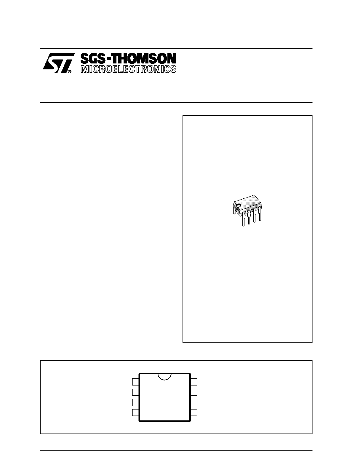
TEA2018A
CURRENT MODE SWITCHING
DIP8
(Plastic Package)
ORDER CODE : TEA2018A
PINCONNECTIONS
OSCILLATOR
COLLECTOR CURRENT SENSING
NEGATIVE SUPPLY VOLTAGE
May 1993
GROUND
1
2
3
4
8
ERROR AMPLIFIER NON-INVERTING INPUT
7
DEMAGNETIZATION SENSING
6
POSITIVE SUPPLY VOLTAGE
5
OUTPUT
2018A-01.EPS
1/7
TEA2018A
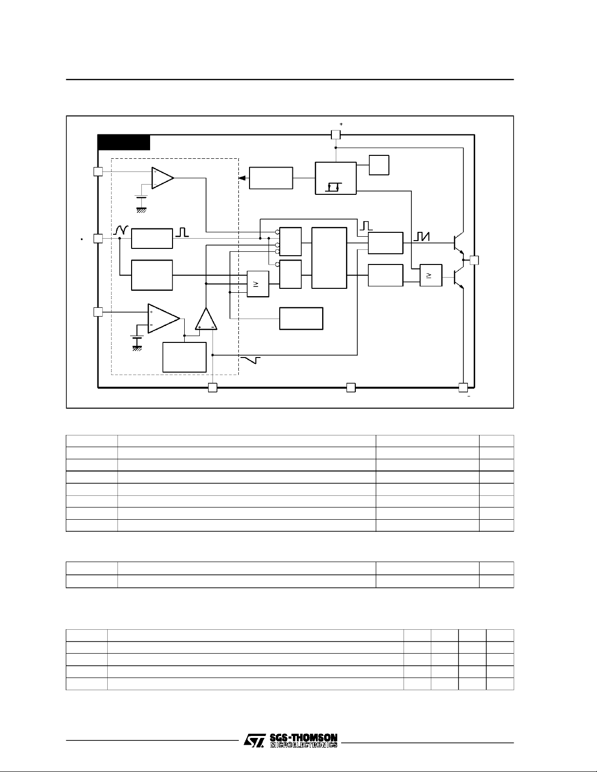
BLOCK DIAGRAM
TEA2018A
7
I
S
DEMAGNETIZATION
SENSING
INTERNAL
BIAS
V
CC
”Good”
V
CC
6
V
CC
MONITORING
V
REF
2.4V
Undervoltage0.1V
2.4V
OSCILLATOR1
MAXIMUM
DUTYCYCLE
70%
COMPARATOR
G ≅ 50
-1V
VOLTAGE
LIMITATION
I
SENSE
&
FLIP-FLOP
&
1
THERMAL
SHUTDOWN
3
GROUND
Ic
RECOPY
DELAY
500ns
5
OUTPUT
1
42
V
CC
RC
tt
8
ABSOLUTE MAXIMUM RATINGS
Symbol Parameter Value Unit
V
+ Positive Supply Voltage 15 V
CC
V
- Negative Supply Voltage -5 V
CC
I
(peak) Peak Output Current (duty cycle < 5%) ±1A
O
I
I
T
T
oper
T
stg
Input Current (Pin 3) ±5mA
Junction Temperature +150
j
Operating Ambient Temperature Range -20, +70
Storage Temperature Range -40, +150
o
C
o
C
o
C
2018A-02.EPS
2018A-01.TBL
THERMALDATA
Symbol Parameter Value Unit
R
th (j-a)
Junction-ambient Thermal Resistance 80
o
ELECTRICAL OPERATINGCHARACTERISTICS
=25oC, potentials referenced to ground (unless otherwise specified) (see testcircuit)
T
amb
Symbol Parameter Min. Typ. Max. Unit
V
+ Positive Supply Voltage 6.6 8 15 V
CC
V
- Negative Supply Voltage -1 -3 -5 V
CC
2/7
V
CC(start)
V
CC(stop)
Minimum Positive Supply Voltage required for starting (VCC+ rising) 6 6.6 V
Minimum Positive Voltage below wich device stopsoperating (VCC+ falling) 4.2 4.9 5.6 V
C/W
2018A-02.TBL
2018A-03.TBL
TEA2018A
ELECTRICAL OPERATINGCHARACTERISTICS
=25oC, potentials referenced to ground (unless otherwise specified) (see testcircuit)
T
amb
Symbol Parameter Min. Typ. Max. Unit
∆V
+ Hysteresis on VCC+ Threshold 0.7 1.1 1.6 V
CC
I
CC(sb)
V
th(IC)
R
V
τ
max
A
I
V
∆V
∆T
t
OSC
∆f
∆T
∆f
∆V
t
on(min)
Stand-by Supply Current before starting (VCC+<V
) 1 1.6 mA
CC(start)
Current Limitation Threshold Voltage (Pin 3) -1100 -1000 -880 mV
Collector Current Sensing Input Resistance 1000 Ω
(IC)
Demagnetization Sensing Threshold 75 100 125 mV
7(th)
I
Demagnetization Sensing Input Current (Pin7 = 0V) 1 µA
S
Maximum Duty Cycle 60 70 %
ErrorAmplifier Gain 50
V
+ Error Amplifier Input Current (non-inverting input) 2 µA
I
Internal Reference Voltage 2.3 2.4 2.5 V
REF
REF
ReferenceVoltage Temperature Drift 10
-4
Oscillator Free-running Period ( R = 59kΩ, C = 1.2nF) 44 48 52 µs
OSC
Oscillator Frequency Drift with Temperature (V
OSC
Oscillator Frequency Drift with VCC+ (+8V < VCC+ < +14V) 0.5 %/V
CC
+ = +8V) 0.05 %/oC
CC
Minimum Conducting Time (Ct= 1nF) 2 µs
V/oC
2018A-04.TBL
RECOMMENDEDOPERATINGCONDITIONS
Symbol Parameter Min. Typ. Max. Unit
V
+ Positive Supply Voltage 8 V
CC
V
- Negative Supply Voltage -3 V
CC
I
Output Current 0.5 A
O
f
oper
Operating Frequency 30 kHz
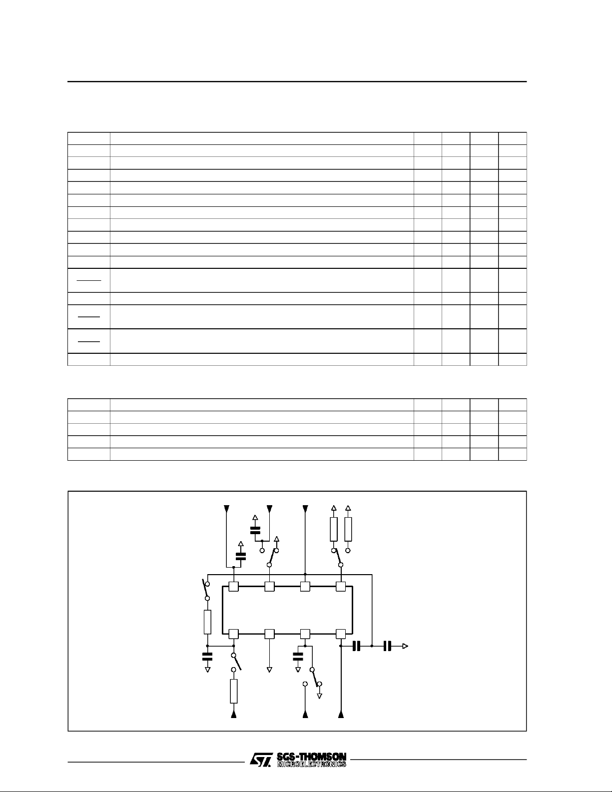
TEST CIRCUIT
V8 V7 V6
10
Ω
4321
470nF
22nF
59k
1%
1.2nF
1%
470
22nF
22nF
8765
Ω
TEA2018A
4.7nF
Ω
2018A-05.TBL
100Ω
V1 V3 V4
2018A-03.EPS
3/7

TEA2018A
GENERALDESCRIPTION
(see applicationnote AN-086)
OperatingPrinciples (Figure 1)
On every period, the beginning of the conduction
time of the transistor is triggered by the fall of the
oscillatorsawtoothwhich acts as clock signal. The
period T
(T
osc
is givenby : T
osc
in seconds,Ctin Farad, Rtin Ω)
≅ 0.66 Ct(Rt+ 200)
osc
The end of the conduction time is determinedby a
signal issued from comparing the following signals :
a) the sawtooth waveform representing the
collector current of the switching transistor,
sampledacross the emitter shunt resistor,
b) the outputof the erroramplifier.
Base Drive
- Fast turn-on : On each period, a current pulse
ensuresfast transistor switch-on.
This pulse performs also the t
on(min)
function at
the beginning of theconduction.
- Proportionalbase drive : Inorder to save power,
the positive base current afterthe starting pulse
becomesan image of the collectorcurrent.
I
C
The ratio
isprogrammedas follows Figure2) :
I
B
TEST CIRCUIT
I
R
C
B
=
I
R
B
e
- Efficient and fast switch-off : When the positive
base driveis removed, 1ms(typically) will elapse
before the application of negative current therefore allowing a safe and rapid collector current
fall.
Safety Functions
- Overload & short-circuit protection : When the
voltage applied to pin 3 exceeds the current
limitation threshold voltage [V
)], the output
th(Ic
flip-flopis reset andthe transistoris turned off.
The shuntresistorR
mustbecalculatedso asto
e
obtain the current limitation thresholdon pin 3at
the maximumallowable collectorcurrent.
- Demagnetizationsensing:This functiondisables
any newconductioncycleof thetransistoraslong
as thecore is not completelydemagnetized.
When not used, pin 7 must be grounded.
-t
on(max)
: Outside the regulation area and in the
absence of current limitation, the maximum conduction time is set atabout 70 % of theperiod.
-t
: Aminimum conducting time is ensured
on(min)
during each period(see Figure 2)
- Supply voltage monitoring : The TEA2018Awill
stop operating if V
thresholdlevel V
CC
CC(stop)
+
on pin 6 falls below the
V
REF
ERROR
AMPLIFIER
ERROR
SIGNAL
OSCILLATOR
SAW-TOOTH
I (sample)
C
FLIP-FLOP
OUTPUT
OSCILLATOR
COMPARATO R
I SENSE
C
FLIP-FLOP
S
R
Re
V
i
OUTPUT
FILTER
I
C
Q
t
Errorsignal
t
t
LOAD
2018A-04.EPS - 2018A-05.EPS
4/7

Figure2
R
TEA2018A
5
B
I
B
3
R
e
SCHEMATICS OF INPUTS AND OUTPUTS
TEA2018A
I
C
COLLECTOR
CURRENT
0
I
I
C
B
t
on(min)
BIAS
CURRENT
I
B
0
I
C
t
R
B
I
C
R
e
t
2018A-06.EPS
DISCH.
+
E
50µA
7.5kΩ
V
CC
7.5kΩ15kΩ
V
Is
ref
V H = 0.66 V
th
V L = 0.33 V
Vd + 0.1V
CC
CCth
2kΩ
+
V
CC
V
CC
1kΩ
1kΩ
Vo
15kΩ
1kΩ
OSC.
GND Ic
-
V
CC
2018A-07.EPS
5/7

TEA2018A
StartingProcess (Figure 3)
Prior to starting, a low current is drawn from the
high voltage source through a high valueresistor.
This current charges the power supply voltage
capacitorof the device.
No output pulses are available before the voltage
on pin6 hasreached the thresholdlevel [V
CC(start)
Figure3 : NormalStart-up Sequence
+
V
CC
6V
4.9V
V
+
CC
V (start)
CC
V (stop)
CC
t
V
rising].
CC
During this time the TEA2018A draws only 1mA
(typically). When the voltage on pin6 reaches this
threshold,base drivepulses appear.
The energy drawn by these pulses tends to discharge the power supply storage capacitor. However a hysteresisof about 1.1V (typically) (∆ V
,
is implemented to avoidthe device from stopping.
Figure4 : t
t (µs)
on (min.)
ON (min.)
versusC
t
12
10
8
6
4
2
12345678910
2018A-08.EPS
C (nF)
t
CC
)
2018A-09.EPS
TYPICALAPPLICATION
4 x 1N4007
0.1µF
RF Filter
2 x 12mH
0.1µF
0.5A
220 V
AC
Maximum Power ≅ 30W
Operating Frequency≅30kHz
47µF
385V
4.7µF4.7kΩ
22kΩ
Ω
1k
8765
47kΩ
TEA2018A
1.2nF
100
Ω
1N4148 68Ω
220µF
16V
10µF150Ω
4321
3.9V
1N414815Ω
4.7kΩ
47µF
R
8.2Ω
BUV
46A
BYW98-50
1000µF
BYW98-50
BA
159
B
BA
159
R
1
2.2kΩ
3W
1kΩ 3W
1nF
1kV
e
Ω
Primary Ground
SecondaryGround
+12V
+5V
4700µF
2018A-10.EPS
6/7

PACKAGE MECHANICAL DATA
8 PINS - PLASTICDIP
b
Z
TEA2018A
e4
I
A
L
a1
B
B1
e
e3
D
Z
E
b1
Dimensions
8
14
Millimeters Inches
Min. Typ. Max. Min. Typ. Max.
5
F
A 3.32 0.131
a1 0.51 0.020
B 1.15 1.65 0.045 0.065
b 0.356 0.55 0.014 0.022
b1 0.204 0.304 0.008 0.012
D 10.92 0.430
E 7.95 9.75 0.313 0.384
e 2.54 0.100
e3 7.62 0.300
e4 7.62 0.300
F 6.6 0260
i 5.08 0.200
L 3.18 3.81 0.125 0.150
Z 1.52 0.060
Information furnished is believed to be accurate and reliable. However, SGS-THOMSON Microelectronics assumes no responsibility
for the consequences of use of suchinformation nor for any infringement of patents or other rights of third parties which may result
from its use. No licence is granted by implication or otherwiseunder anypatent or patent rights of SGS-THOMSON Microelectronics.
Specifications mentioned in this publication are subject to change without notice. This publication supersedes and replaces all
information previously supplied.SGS-THOMSON Microelectronics products are not authorized for use as critical components in life
support devices or systems without express written approval of SGS-THOMSON Microelectronics.
PM-DIP8.EPS
DIP8.TBL
1994 SGS-THOMSON Microelectronics - All Rights Reserved
Purchase of I
2
I
C Patent. Rights to usethese components in a I2C system,is granted provided that the system conforms to
2
C Components of SGS-THOMSON Microelectronics, conveys a license under the Philips
2
the I
C Standard Specifications as defined by Philips.
SGS-THOMSON Microelectronics GROUP OF COMPANIES
Australia - Brazil - China - France - Germany - HongKong - Italy - Japan - Korea- Malaysia - Malta - Morocco
The Netherlands - Singapore - Spain - Sweden - Switzerland - Taiwan - Thailand - United Kingdom - U.S.A.
7/7
 Loading...