

SGS Thomson Microelectronics TEA2014A Datasheet
.
1 VIDEO OUTPUT 75Ω-1V
SWITCHED
.
1 SWITCHEDVIDEOOUTPUT 2V
.
VIDEOCROSSTALK : 50dB TYPICAL
.
SHORT CIRCUIT PROTECTION OF INPUTS
ANDOUTPUTS
.
CLAMPEDVIDEO INPUTS
PP
PP
TEA2014A
VIDEO SWITCH
NOT
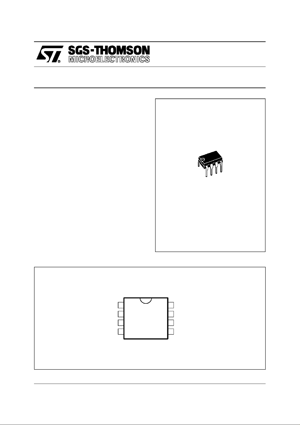
DIP8
(Plastic package)
ORDER CODE : TEA2014A
DESCRIPTION
This integrated circuit providesall video switching
allowingconnectionsbetweentheperi TV plugand
video sections in the TV set. The TEA2014A is
suppliedin a DIP8.
PINCONNECTIONS
GROUND
75ΩVIDEO OUTPUT
INTERNAL VIDEO INPUT
NOT TO BE USED
1
2
3
4
8
EXTERNAL VIDEO INPUT
7
SUPPLY VOLTAGE
6
SWITCHED VIDEO OUTPUT
5
SWITCHING INPUT
2014A-01.EPS
May 1996
1/4

TEA2014A
ABSOLUTE MAXIMUM RATINGS
Symbol Parameter Value Unit
V
CC
T
oper
T
T
stg
– Minimum DC Load Resistor PIN6
THERMALDATA
Symbol Parameter Value Unit
R
th (j-a)
ELECTRICAL CHARACTERISTICS
=+25°C, VCC= 9 V (unless otherwisespecified)
T
amb
Symbol Parameter Min. Typ. Max. Unit
V
CC
I
CC
I
CC
P
tot
INPUTS (pin8 and pin3)
– Internal Video Input Swing from Picture IF (positive Video) – – 4.5 Vpp
– Internal Video Input Impedance (positivevideo) 50 – – kΩ
– Internal Video Input Bias Current (positive video) 6 25 40 µA
– External Video Input Swing (positivevideo) – – 2 Vpp
– External Video Input Impedance (positive video) 50 – – kΩ
SWITCHED OUTPUT (pin 6) - R
– VideoOutput Swing 4 – – Vpp
– VideoOutput Dynamic Impedance – – 25 Ω
– VideoDC Output Voltage (sync. pulselevel note 1) 1.7 2 2.4 V
– VideoBandwith Pin 6 – from Internal Input Pin3 (– 1 dB) 6 – – MHz
– VideoBandwith Pin 6 – from External Input Pin 8 (– 3 dB) 6 – – MHz
– Output Gain Pin 6 – Pin 8 +5 +6 + 7 dB
– Output Gain Pin 6 – Pin 3 – 1 – 0.5 0 dB
EXTERNAL OUTPUT (pin2) - R
– VideoOutput Swing 2.2 – – Vpp
– VideoOutput Dynamic Impedance – 10 – Ω
– VideoDC Output Voltage (sync. pulselevel , note) 1.7 2 2.4 V
– VideoBandwidth (– 1dB) 6 – – MHz
– VideoOutput Gain (pin2 – pin 3) – 1.8 – 1 – 0.4 dB
SWITCHING INPUT (pin 5)
– SwitchingInput Unactive Low Level or Unconnected Pin(TV receiving) 0 – 3 V
– SwitchingInput Active Level (ext. receiving) 7 – V
– SwitchingInput Impedance 10 – – kΩ
Note : Use a video signal witha synchro pulse in order to make the clamp work in acorrect way.
(75Ω to the ground and 10µF in series).
Supply Voltage 18 V
Operating Temperature
with Load > 150 Ω onPIN 2
with Load = 75 Ω on PIN2
Junction Temperature – 40, + 150 °C
j
0, + 100
0, + 70
Storage Temperature – 40, + 150 °C
600
Minimum DC Load Resistor PIN2
75
Junction-ambient Thermal Resistance Typ. 90 °C/W
Supply Voltage Range 8 – 14 V
Supply Current (no loadon Pin 2 and Pin 6) – – 20 mA
Supply Current (with 75 Ω Pin 2.1, with 600 Ω betweenPin 6.1) – 45 – mA
Total Power Dissipation with Load – 400 – mW
= 600 Ω
LOAD
=75Ω
LOAD
CC
°C
Ω
Ω
2014A-01.TBL
2014A-02.TBL
V
2014A-03.TBL
2/4
 Loading...