

SGS Thomson Microelectronics TDF1737, TDE1737 Datasheet
INTERFACE CIRCUIT - RELAY AND LAMP-DRIVER
.HIGH OUTPUT CURRENT
.ADJUSTABLE SHORT-CIRCUIT PROTEC-
TION
.THERMAL PROTECTION WITH HYSTERESIS
TO AVOID THE INTERMEDIATE OUTPUT LEVELS
.LARGE SUPPL Y VOL TAGE RANGE : + 8 V t o
+ 45 V
DESCRIPTION
The TDE1737-TDF1737 is a monolithic amplifier
designed for high c urr e n t and high voltage app lic ations, specific all y to drive lam ps , relays and con trol
of stepper mot or s.
This device is essentially blow-out proof. Current
limiting is available to limit the peak output current
to a safe value, the adjustment only requires one external res istor. In addi tion, thermal sh ut down is provided to keep the I.C. from overheating. If internal
dissipation becomes too great, the driver will shut
down to prevent excessive heating.
The output is also protected against short-circuits
with the positive po wer s upply .
The device operates over a wide range of supply
voltages f r om sta n dar d ± 1 5 V op erationa l ampli fier
supplies down to the single + 12 V or + 24 use d for
industrial electronic systems.
ORDER CODES
Part
Number
TDE1737
TDF1737
Example : TDE1737DP
Temperature
– 25 °C to + 85 °C
– 40 °C to + 85 °C
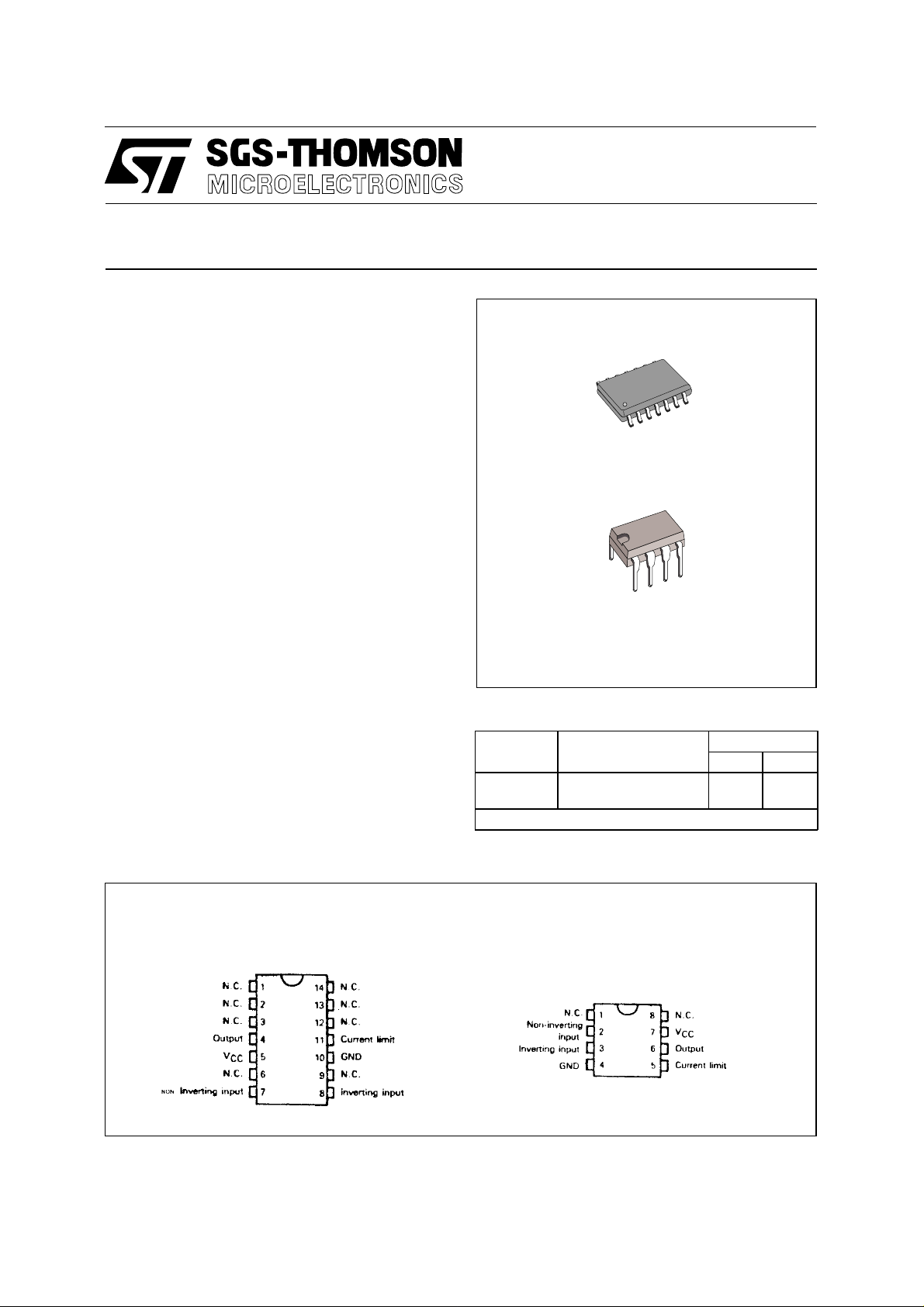
SO14
FP SUFFIX
MINIDIP
DP SUFFIX
Range
TDE17 37
TDF1737
Package
DP FP
•
•
•
•
PIN CONNECTIONS (t op views)
SO-1 4
October 199 1
MINIDIP
1/7
TDE1737 - TDF1737
ABSOLUTE MAXIMUM RATINGS
Symbol Parameter Value Unit
Supply Voltage 50 V
V
s
V
Input Voltage 50 V
I
Differential Input Voltage 50 V
V
ID
I
Output Current 1000 mA
O
Power Dissipation Internally Limited W
P
tot
T
T
T
THERMAL CHARACTERISTICS
Symbol Parameter Value Unit
R
R
Operating Free–air Temperature Range for TDE1737 – 25 to + 85 °C
oper
Operating Free–air Temperature Range for TDF1737 – 40 to + 85 °C
oper
Storage Temperature Range – 65 to + 150 °C
stg
Maximum Junction-case Thermal Resistance MINIDIP 50 °C/W
th(j -c)
Maximum Junction-ambient Thermal Resistance
th(j -a)
120 °C/W
MINIDIP
Junction-ceramic Substrate (case glued to substrate) SO14 90 °C/W
ELECTRICAL CHARACTERISTICS
TDE1737 – 25 °C ≤ T
≤ + 85 °C, + 8 V ≤ VCC ≤ + 45 V, IO ≤ 300 mA, Tj ≤ + 150 °C
amb
(unless otherwise specified)
TDF1737 – 40 °C ≤ T
Symbol Parameter Min. Typ. Max. Unit
Input Offset Voltage – (note 1) – 2 50 mV
V
IO
I
Input Bias Current – 0.1 1.5 µ A
IB
I
Supply Current (VCC = + 24 V, IO = 0) – 3 5 mA
CC
V
V
CC–VO
Notes : 1. The offset voltage given is the maximum value of input voltage required to drive the output voltage within 2 V of
Common–mode Input Voltage Range 2 – VCC–2 V
CM
I
Short–circuit Current Limit (RSC = 1.5 Ω, T
SC
Output Saturation Voltage (output low)
(V
+ – VI – ≥ 50 mV IO = 300 mA, RSC = 0)
I
I
Output Leakage Current
OL
(output high) (V
the ground or the supply voltage.
2. Devices bonded on a 40 cm
≤ + 85 °C, + 8 V ≤ VCC ≤ + 45 V, IO ≤ 300 mA, Tj ≤ 150 °C
amb
= + 25 °C) – 500 – mA
case
– 1 1.5 V
––10µA
= VCC = + 24 V, T
O
2
glass-epoxy printed circuit 0.15 cm thick with 4 cm2 of cooper.
= + 25 °C)
amb
2/7
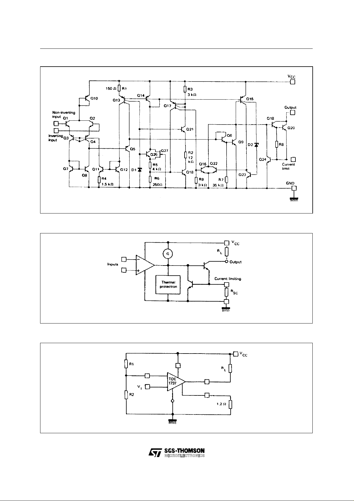
SCHEMATIC DIAGRAM
TDE1737 - TDF1737
SIMPLI FIED SCH EMATIC
TYPICAL APPLICATION -
3/7
 Loading...