

SGS Thomson Microelectronics TDE3237FP, TDE3237DP Datasheet
HIGHOUTPUTCURRENT
ADJUSTABLE SHORT-CIRCUIT PROTECTION
INTERNAL THERMAL PROTECTION WITH
HYSTERESIS TO AVOID THE INTERMEDIATE OUTPUTLEVELS
LARGESUPPLY VOLTAGE RANGE: 8 TO30V
TDE3237
INTELLIGENT POWER SWITCH
ADVANCE DATA
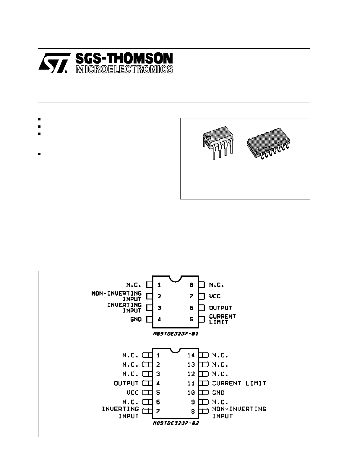
Minidip SO14
DESCRIPTION
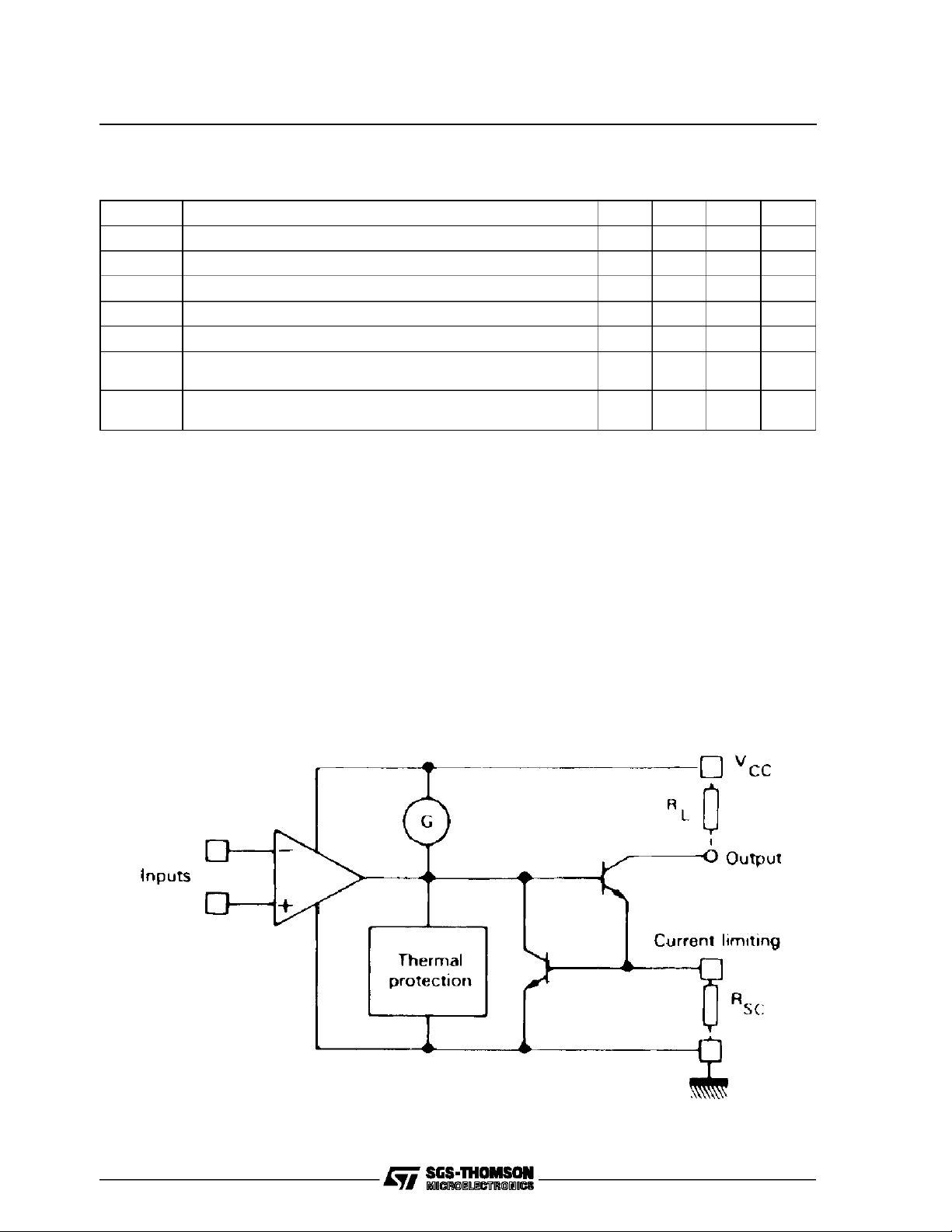
The TDE3237 is a monolithic amplifier designed
for high-current and high-voltage applications,
specIally to drive lamps, relays and stepping motors.
The device is essentially blow-out proof. Current
limiting is availableto limitthe peak output current
to a safe value, the adjustment only requires one
externalresistor. In addition, thermal shut down is
providedto keep the IC fromoverheating.If external dissipation becomes too great, the driver will
PIN CONNECTIONS
ORDERING NUMBERS:
TDE3237DP TDE3237FP
shut down to prevent excessiveheating.
The output is also protected from short-circuits
with the positive power supply.
The device operates over a wide range of supply
voltagesfrom standard±15Voperationalamplifier
supplies down to the single 12V or 24V used for
industrialelectronicsystems.
Minidip
SO14
November 1991
This is advanced information ona new productnow in development or undergoing evaluation. Details aresubject to change without notice.
T is advanced information on a new product now indevelopment or undergoingevaluation. Details are subjectto change without
1/7

TDE3237
ABSOLUTE MAXIMUMRATINGS
Symbol Parameter Value Unit
V
CC
V
V
I
P
T
stg
T
oper
THERMAL CHARACTERISTICS
Symbol Parameter Value Unit
R
th(j-c)
R
th(j-a)
Note : 1. Devices bonded on 40 cm glass-epoxy printed circuit0.15cm thick with 4cm2of copper
Supply Voltage 36 V
Differantial Input Voltage 36 V
ID
Input Voltage 36 V
I
Output Current 500 mA
O
Power Dissipation Internally Limited W
tot
Storage Temperature Range – 65 to + 150 °C
Operating Free-air Temperature Range – 25 to + 85 °C
Maximum Junction-case Thermal Resistance (note 1) Minidip 50 °C/W
Maximum Junction-ambient Thermal Resistance (note 1) Minidip 120 °C/W
Junction-ceramic Substrate (case gluedto substrate) SO14 90 °C/W
Junction-ceramic Substrate (case gluedto substrate, substrate temperature
maintened constant) SO14 65 °C/W
SCHEMATICDIAGRAM
2/7
TDE323 7
ELECTRICAL CHARACTERISTICS T
= – 25 to +85 °C, VCC=8to≤30 V, unlessotherwise speci-
amb
fied (note 1).
Symbol Parameter Min. Typ. Max. Unit
V
I
IB
I
CC
V
CM
I
SC
V
CC–VO
I
OL
Notes :
2) Foroperating athigh temperature, theTDE3237, must bederatedbased on a+150 C maximum junction temperature anda junction-ambient
thermalas showed in the thermal characteristics data base.
3) The offsetvoltage given is the maximum value of input voltage required to drive the outputvoltage within 2 V of the gro und or thesupply
voltage.
Input Offset Voltage - (note 3) – 2 50 mV
IO
Input Bias Current – 0.1 1.5 µA
Supply Current (VCC= + 24 V, IO=0) –35mA
Common-mode Input Voltage Range 2 – VCC–2 V
Short-circuit Current Limit (T
Output Saturation Voltage (output high)
=0, VI+–VI– ≥ 50 mV, IO= 150 mA
(R
SC
Low Level Output Current
(V
O=VCC
=+24VT
amb
=+25°C, RSC= 3.3 Ω ) – 230 – -mA
case
– 1 1.5 V
– – 100 µA
=+25°C)
SIMPLIFIEDSCHEMATIC
3/7
 Loading...