

SGS Thomson Microelectronics TDE1898R, TDE1897R Datasheet
TDE1897R
TDE1898R
0.5A HIGH-SIDE DRIVER
INDUSTRIALINTELLIGENT POWER SWITCH
PRELIMINARY DATA
0.5A OUTPUT CURRENT
18V TO 35V SUPPLY VOLTAGE RANGE
INTERNALCURRENTLIMITING
THERMALSHUTDOWN
OPENGROUND PROTECTION
INTERNAL NEGATIVE VOLTAGE CLAMPING
TO V
DIFFERENTIAL INPUTS WITH LARGE COM-
MON MODE RANGE AND THRESHOLD
HYSTERESIS
UNDERVO LTAGELOCKOUTWITHHYSTER ESIS
OPENLOAD DETECTION
TWO DIAGNOSTIC OUTPUTS
OUTPUTSTATUS LED DRIVER
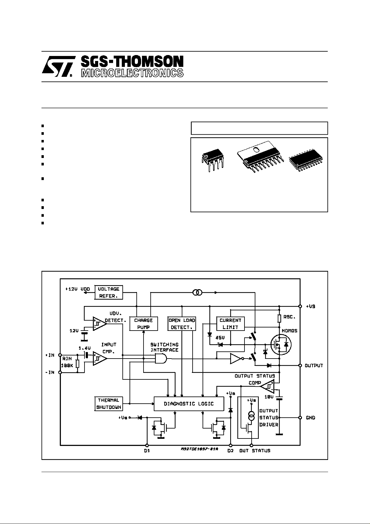
DESCRIPTION
The TDE1897R/TDE1898R is a monolithic Intelligent Power Switch in Multipower BCD Technol-
BLOCKDIAGRAM
- 45V FOR FAST DEMAGNETIZATION
S
MULTIPOWERBCD TECHNOLOGY
Minidip SIP9 SO20
ORDERING NUMBERS:
TDE1897RDP TDE1898RSP TDE1897RFP
TDE1898RDP TDE1898RFP
ogy, for driving inductive or resistive loads. An internal Clamping Diode enables the fast demagnetizationof inductive loads.
Diagnostic for CPU feedback and extensive use
of electrical protections make this device inherently indistructible and suitable for general purpose industrial applications.
October 1995
This is advanced information on a new product now in development or undergoing evaluation. Details are subject to change without notice.
1/12
TDE1897R- TDE1898R
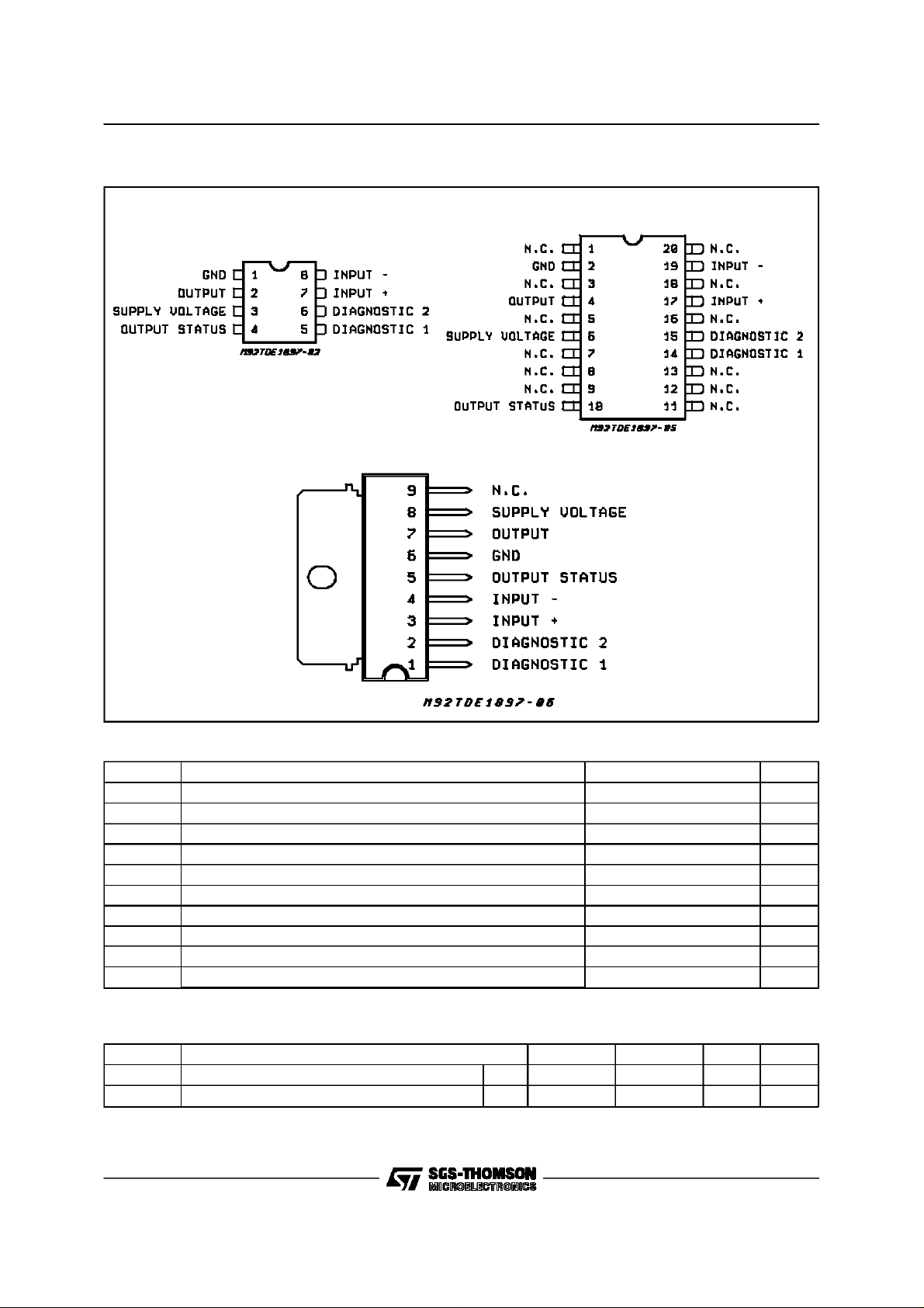
PIN CONNECTIONS (Top view)
SIP9
Minidip
SO20
ABSOLUTE MAXIMUM RATINGS (Minidippin reference)
Symbol Parameter Value Unit
V
V
S–VO
V
V
I
E
P
T
T
S
I
i
O
tot
op
stg
Supply Voltage (Pins 3 - 1) (TW< 10ms) 50 V
Supply to OutputDifferential Voltage. SeealsoVCl3-2(Pins3 - 2) internally limited V
Input Voltage (Pins 7/8) -10 to VS +10 V
i
Differential Input Voltage (Pins 7 - 8) 43 V
i
Input Current (Pins 7/8) 20 mA
Output Current (Pins 2 - 1). See also ISC internally limited A
Energy from Inductive Load(TJ=85°C) 200 mJ
l
Power Dissipation. See alsoTHERMAL CHARACTERISTICS. internally limited W
Operating Temperature Range (T
) -25 to +85 °C
amb
Storage Temperature -55 to 150 °C
THERMALDATA
Symbol Description Minidip Sip SO20 Unit
Thermal Resistance Junction-case Max. 10 °C/W
Thermal Resistance Junction-ambient Max. 100 70 90 °C/W
2/12
R
th j-case
R
th j-amb

TDE1897R - TDE1898R
ELECTRICALCHARACTERISTICS (VS=24V; T
= –25 to +85°C,unless otherwise specified)
amb
Symbol Parameter Test Condition Min. Typ. Max. Unit
3 Supply Voltage for Valid
V
smin
I
> 0.5mA @ V
diag
= 1.5V 9 35 V
dg1
Diagnostics
V
3 Supply Voltage (operative) 18 24 35 V
s
3 Quiescent Current
I
q
V
sth1
V
sth2
V
shys
I
sc
V
don
I
oslk
V
ol
3-2 Internal Voltage Clamp (VS-VO)@IO= -500mA 45 55 V
V
cl
I
old
7-8 Common Mode Input Voltage
V
id
I
out=Ios
=0
Undervoltage Threshold 1 (See fig. 1); T
3 Undervoltage Threshold 2 (See fig. 1); Tamb = 0 to +85°C 15.5 V
Supply Voltage Hysteresis (See fig. 1); T
Short Circuit Current VS= 18 to 35V; RL=1Ω 0.75 1.5 A
3-2 Output Voltage Drop @ I
2 OutputLeakage Current @ Vi=Vil,Vo= 0V 300 µA
2 Low State Out Voltage @ Vi=Vil;RL=∞ 0.8 1.5 V
2 Open Load Detection Current Vi=Vih;T
Range (Operative)
7-8 Input Bias Current Vi= –7 to 15V; –In = 0V –700 700 µA
I
ib
7-8 InputThreshold Voltage V+In > V–In 0.8 1.4 2 V
V
ith
7-8 Input Threshold Hysteresis
V
iths
V
il
V
ih
= 0 to +85°C11 V
amb
= 0 to +85°C 0.4 1 3 V
amb
= 625mA; Tj=25°C
out
@I
= 625mA; Tj= 125°C
out
= 0 to +85°C 0.5 9.5 mA
amb
VS= 18 to 35V,
V
7-8 < 37V
S-Vid
–7 15 V
V+In > V–In 50 400 mV
2.5
4.5
250
400
4
7.5
425
600
Voltage
R
7-8 Diff. InputResistance @ 0 < +In < +16V; –In = 0V
id
@ –7 < +In < 0V; –In= 0V
I
7-8 Input Offset Current V+In = V–In +Ii
ilk
0V < V
<5.5V –Ii
i
–In = GND +Ii
0V < V+In <5.5V –Ii –250
+In = GND +Ii
0V < V–In <5.5V –Ii
V
2 Output Status Threshold 1
oth1
(See fig. 1) 12 V
–20
–75 –25
–100
–50
400
150
+10
–125
–30
–15
+20 µA
+50 µA
Voltage
V
2 Output Status Threshold 2
oth2
(See fig. 1) 9 V
Voltage
V
2 Output Status Threshold
ohys
(See fig. 1) 0.3 0.7 2 V
Hysteresis
I
4 Output Status Source Current V
osd
3-4 Active Output Status Driver
V
osd
Drop Voltage
4 Output Status Driver Leakage
I
oslk
Current
5/6 Diagnostic Drop Voltage D1 / D2 = L @ I
V
dgl
out>Voth1,Vos
Vs–Vos@Ios= 2mA;
T
= -25 to 85°C
amb
V
out<Voth2,Vos
V
= 18 to 35V
S
D1 / D2 = L @ I
5/6 Diagnostic Leakage Current D1 / D2 =H @ 0 < Vdg<V
I
dglk
= 2.5V 2 4 mA
5V
=0V
diag
diag
= 0.5mA
= 3mA
s
25 µA
250
1.5
25 µA
VS= 15.6 to 35V
5/6-3 Clamping Diodes at the
V
fdg
@I
= 5mA; D1 / D2 = H 2 V
diag
Diagnostic Outputs.
Voltage Drop to V
Note Vil < 0.8V, Vih > 2V @ (V+In> V–In); Minidip pin reference.
All test not dissipative.
S
mA
mA
mV
mV
KΩ
KΩ
µA
µA
µA
µA
mV
V
3/12

TDE1897R- TDE1898R
SOURCEDRAIN NDMOS DIODE
Symbol Parameter Test Condition Min. Typ. Max. Unit
2-3 Forward On Voltage @ I
V
fsd
2-3 Forward Peak Current t = 10ms; d = 20% 2 A
I
fp
2-3 Reverse Recovery Time If= 625mA di/dt = 25A/µs 200 ns
t
rr
2-3 Forward Recovery Time 50 ns
t
fr
THERMALCHARACTERISTICS (*)
Θ Lim Junction Temp. Protect. 135 150 °C
T
H
Thermal Hysteresis 30 °C
SWITCHINGCHARACTERISTICS (VS=24V; RL=48Ω) (*)
= 625mA 1 1.5 V
fsd
t
on
t
off
t
d
Turn on Delay Time 100 µs
Turn off Delay Time 20 µs
Input Switching to Diagnostic
100 µs
Valid
Note Vil < 0.8V, Vih > 2V @ (V+In > V–In); Minidip pin reference. (*) Not tested.
Figure1
DIAGNOSTICTRUTH TABLE
Diagnostic Conditions Input Output Diag1 Diag2
Normal Operation L
H
Open Load Condition (I
)L
o<Iold
H
Short to V
S
L
H
Short Circuit to Ground (I
) (**) TDE1897R
O=ISC
TDE1898R
H <H (*) H L
HH
Output DMOS Open L
H
Overtemperature L
H
SupplyUndervoltage (V
supplyvoltage;V
S<Vsth2
S<Vsth1
in the fallingphase of the
inthe rising phaseof the supply
L
H
voltage)
(*) According to the intervention of the current limiting block.
(**) A cold lampfilament,or a capacitive load may activatethe current limiting circuit of the IPS,when theIPS is initially turned on.TDE1897
uses Diag2 to signal such condition, TDE1898 does not.
4/12
L
H
L
H
H
H
H
H
H
L
L
L
H
L
L
L
L
L
L
L
H
H
L
H
H
L
L
H
H
H
H
H
H
H
H
H
H
L
L
L
L
 Loading...