

SGS Thomson Microelectronics TDE1787DP, TDE1787ADP, TDE1767DP, TDE1767ADP Datasheet
INTERFACECIRCUIT(RELAY AND LAMP-DRIVER)
OPENGROUND PROTECTION
HIGHOUTPUTCURRENT
ADJUSTABLESHORT-CIRCUIT PROTECTION
INTERNAL THERMAL PROTECTION WITH
EXTERNALRESET
LARGESUPPLY VOLTAGERANGE
ALARMOUTPUT
INPUTVOLTAGECAN BE HIGHER THAN V
OUTPUT VOLTAGE CAN BE LOWER THAN
GROUND(V
CC-VO≤VCC
[max])
CC
TDE1767, A
TDE1787, A
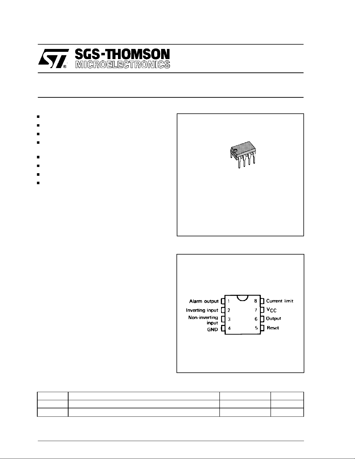
Minidip
DESCRIPTION
The TDE1767,A/TDE1787, Aare a monolithicamplifiers designed for high current and high voltage
applications, specifically to drive lamps, relays,
stepping motors.
The devices are assentially blow-out proof. The
output isprois protectedfromshort-circuits withthe
positive supply or drive. In addition thermal shut
down is provitedto keepthe IC from overheathing.
If internal dissipationbecomes too high, the driver
will shut down to prevent excessive heating. The
output stays null after the overheating is off, if the
reset input is low. If highthe outputwillalternatively
switch-onand off until the overloadis removed.
The devices operates over a wide range voltages
from standard 15 V operational amplifier supplies
to thesingle+6Vor+48Vusedforindustrialelectric
systems. Input voltages can be higher than in the
.
V
CC
An alarm output suitable for driving a LED is
provited. This LED, normally on (if referred to
ground), will die out or flash during an overload
depending on the state of the reset input.
The output is low in open groundconditions.
ORDERING NUMBERS : TDE1767 DP
TDE1767 ADP
TDE1787 DP
TDE1787 ADP
PIN CONNECTION (top view)
THERMALDATA
Symbol Parameter Value Unit
R
th (j - c)
R
th (j- a)
* Devices bonded ona 40 cm2glass-epoxy printed circuit 0.15cm thick with4 cm2of copper.
March 1993
Maximum Junction-case Thermal Resistance 30 °
Maximum Junction-ambient Thermal Resistence 80
C/W
°C/W
1/10

TDE1767,A-TDE1787,A
ABSOLUTEMAXIMUM RATINGS
Symbol Parameter TDE1767A/TDE1787A TDE1767/TDE1787 Unit
V
V
V
l(reset)
I
P
T
T
SCHEMATIC DIAGRAM
Supply Voltage 60 50 V
CC
Input Differential Voltage 60 50 V
ID
V
Input Voltage - 10 to + 60 - 10 to + 50 V
l
I
Output Current 1.3 1.2 A
O
Reset Input Voltage - 0.5 to + 60 - 0.5 to + 50 V
Alarm Output Current - 10 to + 20 - 10 to + 20 mA
OA
Power Dissipation Internally Limited mW
tot
Operating AmbientTemperature
oper
-25to+85 -25to+85
Range
Storage Temperature Range - 65 to + 150 - 65 to + 150
stg
°C
°C
EQUIVALENTSCHEMATIC
2/10

TDE1767,A-TDE1787,A
Figure1.
ELECTRICAL CHARACTERISTICS (Unlessotherwisespecified)
TDE1767A:-25°C≤T
TDE1767:-25°C≤T
TDE1787A:-25°C≤T
TDE1767A:-25°C≤T
Symbol Parameter Min. Typ. Max. Unit
V
I
I
V
I
V
sense
V
O(sat)
I
I
reset
V
th (reset)
Input Offset Voltage - (note 1) 2 50 mV
IO
Power Supply Current (measured on pin 4) mA
CC
Output High (T
Output High (V
Output Low (V
Input Bias Current - 15 100
IB
Common-mode Input VoltageRange
CM
Input Voltage Range (V
V
l
(figure 1, note 2)
Short-circuit Output Current
SC
(V
= + 35 V,t = 10 ms)
CC
= 0.22 Ω
R
SC
R
= 0.33 Ω
SC
Output Limit Sense Voltage: VO=VCC- 2 V,t = 10ms
(V
O=VCC
-2V) :VO= 0 V,t = 10 ms
Output Saturation Voltage(output high V
R
=0,VCC=+30V)
SC
=+25°C
T
j
= + 150 °C
T
j
Output Leakage Current (output low) - - 100
OL
Available Alarm Output Current
I
A
Output Source Current (VAH = V
Output Slnk Current (in thermal shut-down) V
Reset Input Current - 2 40 µ
Reset Threshold - 1.4 - V
- Output Leakage Current (openground) - 10 -
≤ +85°C, + 6 V≤ VCC≤ +55V,Io≤500mA, Tj≤ + 150°C
amb
≤ +85°C, + 6 V ≤ VCC≤ +45V,Io≤500mA, Tj≤ +150°C
amb
≤ +85°C, + 6 V≤ VCC≤ +55V,Io≤300mA, Tj≤ + 150°C
amb
≤ +85°C, + 6 V≤ VCC≤ +45V,Io≤300mA, Tj≤ + 150°C
amb
=+25°C) - 5.8 8
amb
CC=VCC(max),Tj
CC=VCC(max),Tamb
≥ +1V)
ref
= + 150 °C)
=+25°C)
+
l
- 2.5 V)
CC
TDE1787A, TDE1767A
TDE1787, TDE1767
TDE1787A, TDE1767A
TDE1787, TDE1767
TDE1767A
TDE1787A
-
-V
≥50 mV,
l
TDE1787A, TDE1767A
TDE1787, TDE1767
TDE1787A, TDE1767A
TDE1787, TDE1767
= 1.4 V
A
-57
- 1.5 4
1
1
0
0
-
700
-
380
130
120
150
140
-
-
-
1.1
-
1.1
-4
5
10
-
-
-
-
60
45
60
45
-
-
170
165
1
1
1.1
1.2
1.2
1.3
-5
-
-
µA
V
V
mA
mV
V
µA
mA
A
µA
Notes: 1. The offsetvoltage given is the maximum value of different input voltage reguired to drive the output voltage whitin 2 V of the
ground or the supply voltage.
2. Input voltage range is indipendent of the supply voltage.
3/10
 Loading...