

9.5NS TRIPLE HIGH VOLTAGE VIDEO AMPLIFIER
FEATURE
■ TRIPLE CHANNEL VIDEO AMPLIFIER
■ SUPPLY VOLTAGE: 110V TYPICAL
■ RISE AND FALL TIMES: 9.5ns TYPICAL
■ BANDWIDTH: 37MHz TYPICAL
■ 80 VOLTS OUTPUT DYNAMIC RANGE
■ LOW POWER CONSUMPTION
■ WELL MATCHED WITH TDA9210 PREAMP
■ FULL PIN COMPATIBILITY WITH TDA9536
DESCRIPTION
The TDA9535 is a triple video amplifier with high
voltage Bipolar/CMOS/DMOS technology (BCD)
for use in color monitor application. Used with
TDA9210 preampin DC coupled mode, it provides
for a low component, high performance and cost
effective system solution. Other features include
1024 x 768 displays, pixel clock frequencies up to
75MHz, and DC or AC coupling designs.
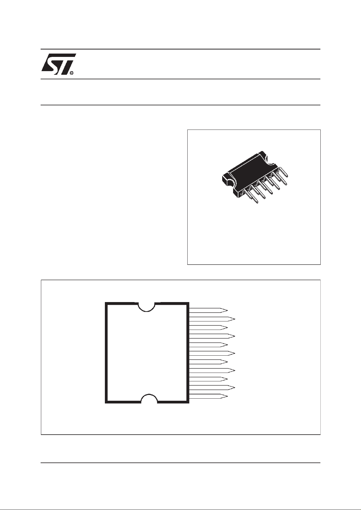
TDA9535
PRELIMINARY DATA
CLIPWATT11
(Plastic Package)
ORDER CODE: TDA9535
PIN CONNECTIONS
11
10
9
8
7
6
5
4
3
2
1
OUT3
GND3
IN3
V
CC
IN2
GND2
OUT2
V
DD
IN1
GND1
OUT1
Version 3.2
March 2000 1/9
This ispreliminary information on a new product in development or undergoing evaluation. Detailsare subject to change without notice.
1
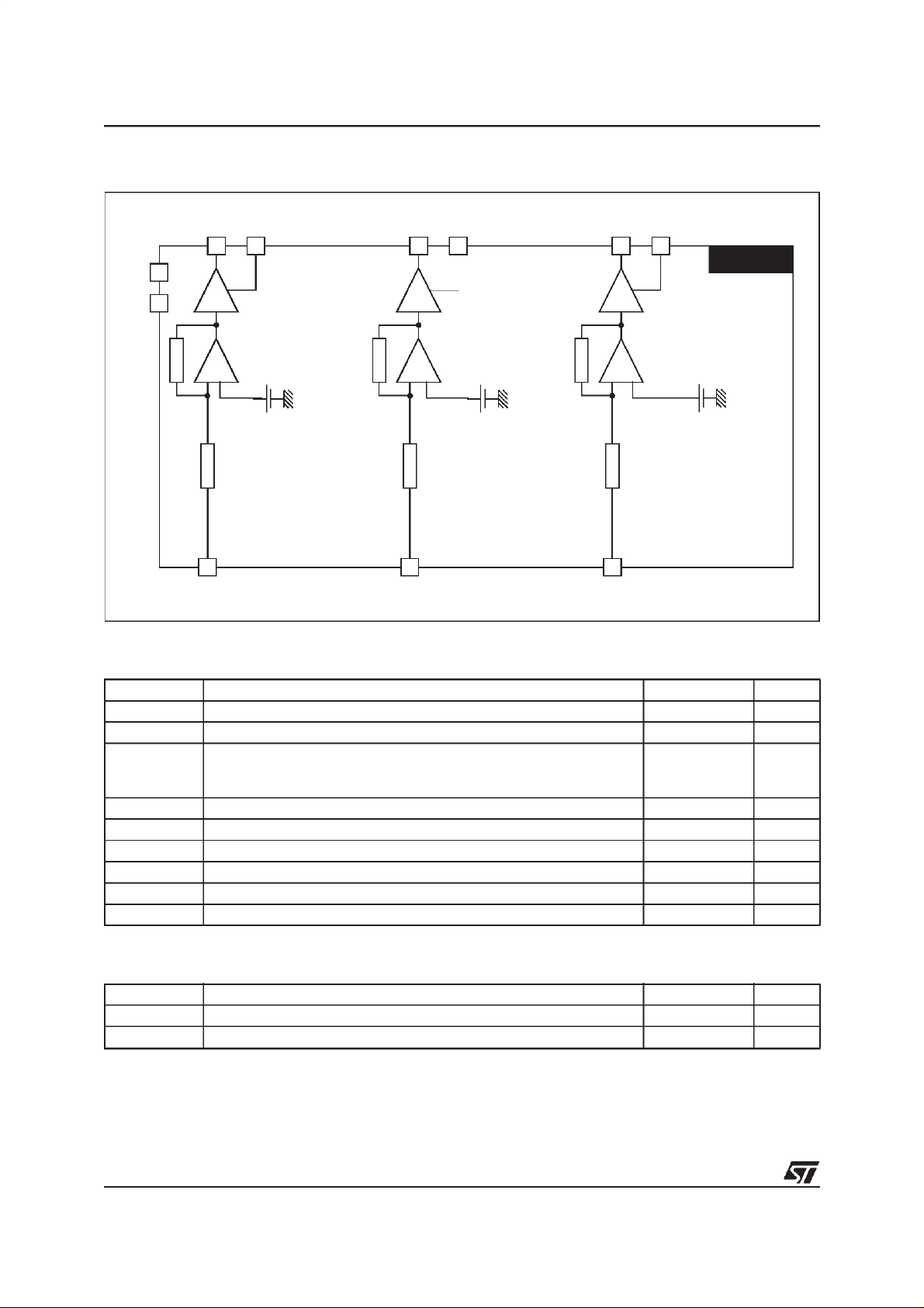
TDA9535
BLOCK DIAGRAM
1
2
V
DD
4
V
8
CC
Vref
37 9
ABSOLUTE MAXIMUM RATINGS
GND2
OUT2GND1OUT1
OUT3 GND3
1165
10
TDA9535
Vref
IN3IN2IN1
Vref
Symbol Parameter Value Unit
V
V
V
V
V
T
DD
CC
ESD
I
OD
I
OG
IMax
I Min
T
J
STG
High Supply Voltage 120 V
Low Supply Voltage 17 V
ESD Susceptibility
Human Body Model, 100pF. Discharge through 1.5KΩ
EIAJ Norm, 200pF. Discharge through 0Ω
2
250
Output Source Current (pulsed < 50µs) 80 mA
Output Sink Current (pulsed < 50µs) 80 mA
Maximum Input Voltage 15 V
Minimum Input Voltage - 0.5 V
Junction Temperature 150 °C
Storage Temperature -20 + 150 °C
THERMAL DATA
Symbol Parameter Value Unit
R
R
th (j-c)
th (j-a)
Junction-Case Thermal Resistance (Max.) 3 °C/W
Junction-Ambient Thermal Resistance (Typ.) 35 °C/W
kV
V
2/9
TDA9535
ELECTRICAL CHARACTERISTICS
(VCC = 12V, VDD = 110V, Tamb = 25 °C)
Symbol Parameter Test Conditions Min Typ Max Unit
V
DD
V
CC
I
DD
I
CC
/dV
dV
OUT
dV
/dTemp
OUT
V
OUT SATH
V
OUTSATL
AV
R
E
lin
OS Overshoot 5 %
Lf
∆g/g
R
IN
BW Bandwidth at -3dB
t
R,tF
Lf CT
Hf CT
High Supply Voltage (Pin 4) 110 115 V
Low Supply Voltage (Pin 8) 10 12 15 V
High Voltage Supply Internal DC Cur-
rent
Low Voltage Supply Internal DC Current
High Voltage Supply Rejection V
DD
Output Voltage Drift Versus
Temperature for anyChannel
Max. Output Voltage
Min. Output Voltage
Typical Video Gain V
Linearity Error 17<V
Low Frequency Gain Matching V
Video Input Resistor V
Rise and Fall Time
Low Frequency Crosstalk
High Frequency Crosstalk
V
= 50V
OUT
15
40
= 50V 0.5 %
OUT
V
= 80V 15
OUT
V
-
I0=-60mA, (1)
=60mA, (1)
I
0
= 50V 20
OUT
OUT<VDD
= 50V, f=1MHz 5 %
OUT
= 50V 2 KΩ
OUT
=50V,C
V
OUT
=200Ω, ∆V
R
P
=50V,C
V
OUT
=200Ω, ∆V
R
P
V
=50V,C
OUT
=200 Ω,∆V
R
P
-15V 5 8 %
=8pF
LOAD
=20V
OUT
=8pF
LOAD
=40V
OUT
=8pF
LOAD
=20V
OUT
f=1MHz
f = 20MHz
DD
6.5
11
37 MHz
9.5 ns
50
32
mA
mA
mV/
°C
V
V
dB
dB
Note: 1 Pulsed current width < 50µs
3/9

TDA9535
TYPICAL APPLICATION
PC Board Lay-out
The best performance is obtained with a carefully
designed HF PC board, especially for the output
and input capacitors.
Rise/fall time and bandwidth are measured on
a 10pF load. The best rise/fall times and bandwidth results will be obtained with low Rp resistor
value while the best CRT arcing protection will be
obtained by a high Rp resistor value. Finally a value between 150 and 220Ω is a good compromise.
Power Dissipation
The power dissipation is the sum of the DC and
the dynamic dissipation.
As the feedback resistors are integrated, the DC
power dissipation (capacitive load) can be estimated by:
P
STAT=VDD.IDD+VCC.ICC
The dynamic dissipation in the worst case (full
bandwidth and black pixel/white pixel picture
(note 2) is:
P
=3VDD.CL.V
DYN
OUT(PP)
.f.K
where f is the video frequency and K the active line
duration / total duration.
Example:
for VDD= 110V, VCC= 12V, V
IDD= 15mA, ICC= 40mA, f
CL= 8pF and K = 0.72.
We have: P
Therefore: P
Note: 2 This worst thermal case must only be
considered for TJmax calculation.
Nevertheless, during the average life of the
circuit, the conditions are very close to the
white picture conditions.
= 2.13W and P
STAT
=4.41W.
tot
VIDEO
=40VPP,
OUT
= 30MHz,
DYN
= 2.28W
75Ω
75
75Ω
V
CC
V
CC
V
DD 110V
V
DD
48
TDA9535
R
3
IN1
Ω
7
IN2
9
IN3
OUT1
1
2
GND1
OUT2
5
6
GND2
OUT3
11
10
GND3
P
C
L
R
P
C
L
R
P
C
L
4/9

TDA9535
Figure 1. TDA9535/9536 - TDA9210 - DemonstrationBoard: Silk Screen and Trace (scale 1:1)
5/9

TDA9535
Figure 2. TDA9535/9536 - TDA9210 - DemonstrationBoard Schematic
F2(2)
R23 150R
L3
R22
0.33uH
120R
R28
TDA9535/36
Heater
101112
F1(2)
C14
H1BGND
G2
J8
C19
8
R
GND_CRT
110V
J7
7
G2
C21
10nF/2KV
G1 G
GND
100nF/250V
56
R27 150R
1
10nF/400V
9
H2
J5
10R
E
0.33uH
120R
GND3
R15 150R
110V
D7(2)
FDH400
L2
R31
S_R
R14
47uF
C8
12V
C7(1)
100nF
VCC
IN2
IN3
47pF
C24
R33
24R
0.33uH
120R
GND2
D9(2)
FDH400
110V
110V
R32
S_R
4.7uF/150V
C18
R26(2) 39R
C10(1)
100nF/250V
1
2345678910
VDD
47pF
24R
OUT1
GND1
IN1
C25
47pF
R24
24R
OUT2
R7 150R
D2(2)
FDH400
110V
L1
R30
S_R
R6
transientresponse optimisation
D
11
OUT3
U2
C23
R29
F4(2)
11Wednesday,February16,2000
E
4.7nF/1kV
C20
Version1.4
CRT3withTDA9210+ TDA9535/36
Custom
Title
Size DocumentNumber Rev
Date: Sheet of
G1
D
HsOut
R20 100R
R1 100R
C1(1)
8V
100pF
VsOut
R18 100R
R11 2R7
U1
R4
2R7
5V
5V
D1
J1
4 4
C
B
A
12
20
1
R2 15R
C3 100nF
1N4148
GRN
15R/33R
R13 15R/33R
R9
17
18
19
HS
BLK
OUT1
VCCP
IN1
ABL
IN2
GNDL
2
3
4
R8 15R
C9(1) 100nF
C4 100nF
D4
1N4148
5V
D5
1N4148
5V
D3
1N4148
D6
R5
75R
R3
75R
BLU
RED
R17 15R/33R
5V
C5(1)100nF
15
16
OUT2
GNDP
IN3
GNDA
5
6
R12 15R
C22(1)100nF
5V
C6 100nF
D8
1N4148
1N4148
R10
75R
1234567891011
Video
R21 2K7
R19 2K7
12
13
14
SCA
OUT3
VCCA
OSD1
7
8
9
R16 2R7
3 3
SCL
OSD2
10 11
OSD3 FBLK
5V
C13
100pF
TDA9210
110V
J10
I2C
123
4
C12
100pF
1: All capacitorsfollowedby (1) are decoupling capacitors
which must be connected as close as possible to the device
2: The purposeof all componentsfollowed by (2) is to ensure a
good protectionagainst overvoltage(arcingprotection)
Notes:
VsOut
G1
Heater
C15
C17
12V
47uF
47uF
C16
47uF
5V
8V
12345
J16
Power
12345
J17
2 2
HsOut
6
Supply
1 1
C
B
A
6/9

PACKAGE MECHANICAL DATA
11 PIN - CLIPWATT
TDA9535
V
L
Dimensions
V1
L3
L2
lead#1
S
G
G2
A
C
R3
M
V1
V1
L1
D
B
V2
V1
V
R3
R3
E
M1
Millimeters Inches
Min. Typ. Max. Min. Typ. Max.
H3
H2
H1
R1
F
G1
A 2.95 3.00 3.05 0.116 0.118 0.120
B 0.95 1.00 1.05 0.037 0.039 0.041
C 0.15 0.006
D 1.30 1.50 1.70 0.051 0.059 0.066
E 0.49 0.515 0.55 0.019 0.020 0.021
F 0.78 0.80 0.88 0.031 0.033 0.034
G 1.60 1.70 1.80 0.063 0.067 0.071
G1 16.90 17.00 17.10 0.665 0.669 0.673
H1 12.00 0.472
H2 18.55 18.60 18.65 0.730 0.732 0.734
H3 19.90 20.00 20.10 0.783 0.787 0.791 ()
L 17.70 17.90 18.10 0.696 0.704 0.712
L1 14.35 14.55 14.65 0.564 0.572 0.576
L2 10.90 11.00 11.10 0.429 0.433 0.437()
L3 5.40 5.50 5.60 0.212 0.216 0.220
M 2.34 2.54 2.74 0.092 0.100 0.107
M1 2.34 2.54 2.74 0.092 0.100 0.107
R 1.45 0.057
R1 3.20 3.30 3.40 0.126 0.130 0.134
R2
R
7/9

TDA9535
Dimensions
R2 0.30 0.012
R3 0.50 0.019
S 0.65 0.70 0.75 0.025 0.027 0.029
V 10deg. 10deg.
V1 5deg. 5deg.
V2 75deg. 75deg.
“H3 and L2” do not include mold flash or protrusions
Mold flash or protrusions shall not exceed 0.15mm per side.
Min. Typ. Max. Min. Typ. Max.
Millimeters Inches
8/9

TDA9535
Information furnished is believed to be accurate and reliable. However, STMicroelectronics assumes no
responsibility for the consequences of use of such information nor for any infringement of patents or other
rights ofthird parties which may result from its use. No license is granted by implication orotherwise underany
patent orpatent rights of STMicroelectronics. Specifications mentioned in this publication are subject tochange
without notice. This publication supersedes and replaces all information previously supplied.
STMicroelectronics products are not authorized for use as critical components in life support devices or
systems without express written approval of STMicroelectronics.
The ST logo is a trademark of STMicroelectronics.
2000 STMicroelectronics - All Rights Reserved
Purchase of I
Rights to use these components in a I
2
C Components ofSTMicroelectronics, conveys a license under the PhilipsI2C Patent.
2
C system, is granted provided that the system conforms to the I2C
Standard Specifications as defined by Philips.
STMicroelectronics GROUP OF COMPANIES
Australia - Brazil - China - Finland -France -Germany - Italy - Japan - Korea - Malaysia - Malta - Mexico -Morocco - The
Netherlands - Singapore - Spain - Sweden - Switzerland - Taiwan - Thailand - United Kingdom - U.S.A.
http://www.st.com
9/9
 Loading...