

7.5NS TRIPLE HIGH VOLTAGE VIDEO AMPLIFIER
FEATURE
❥ TRIPLE CHANNEL VIDEO AMPLIFIER
❥ SUPPORTS DC OR AC COUPLING
APPLICATIONS
❥ BUILT IN VOLTAGE GAIN: 20
❥ RISE AND FALL TIMES: 7.5ns TYPICAL
❥ BANDWIDTH: 50MHz TYPICAL
❥ SUPPLY VOLTAGE: 110V
❥ ADDITIONAL CUT-OFF INPUT CONTROL
DESCRIPTION
The TDA9533 is a triple video amplifier with high
voltage Bipolar/CMOS/DMOS technology (BCD).
It candrive the 3 cathodes of amonitor CRT in DC
or ACcoupling mode.A DCcoupling application is
obtained by connecting a triple DC controlled circuit either on the input pin or on the cut-off pin.
TDA9533
PRELIMINARY DATA
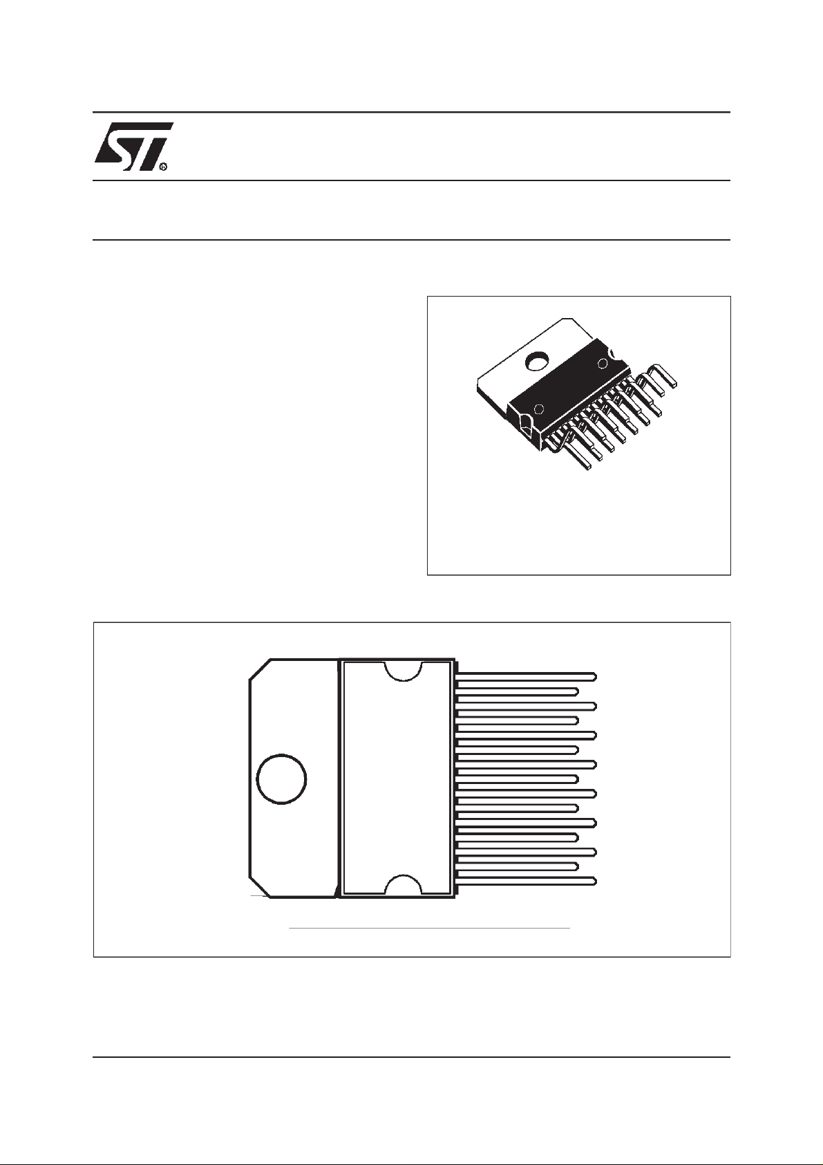
MULTIWATT15
(Plastic Package)
ORDER CODE: TDA9533
PIN CONNECTIONS
OUT3
C.OFF3
GND3
IN3
V
CC
IN2
GND2
GNDS
OUT2
C.OFF2
V
DD
IN1
GND1
C.OFF1
OUT1
Version 3.2
March 2000 1/8
This ispreliminary information on a new product in development or undergoing evaluation. Detailsare subject to change without notice.
1
TDA9533
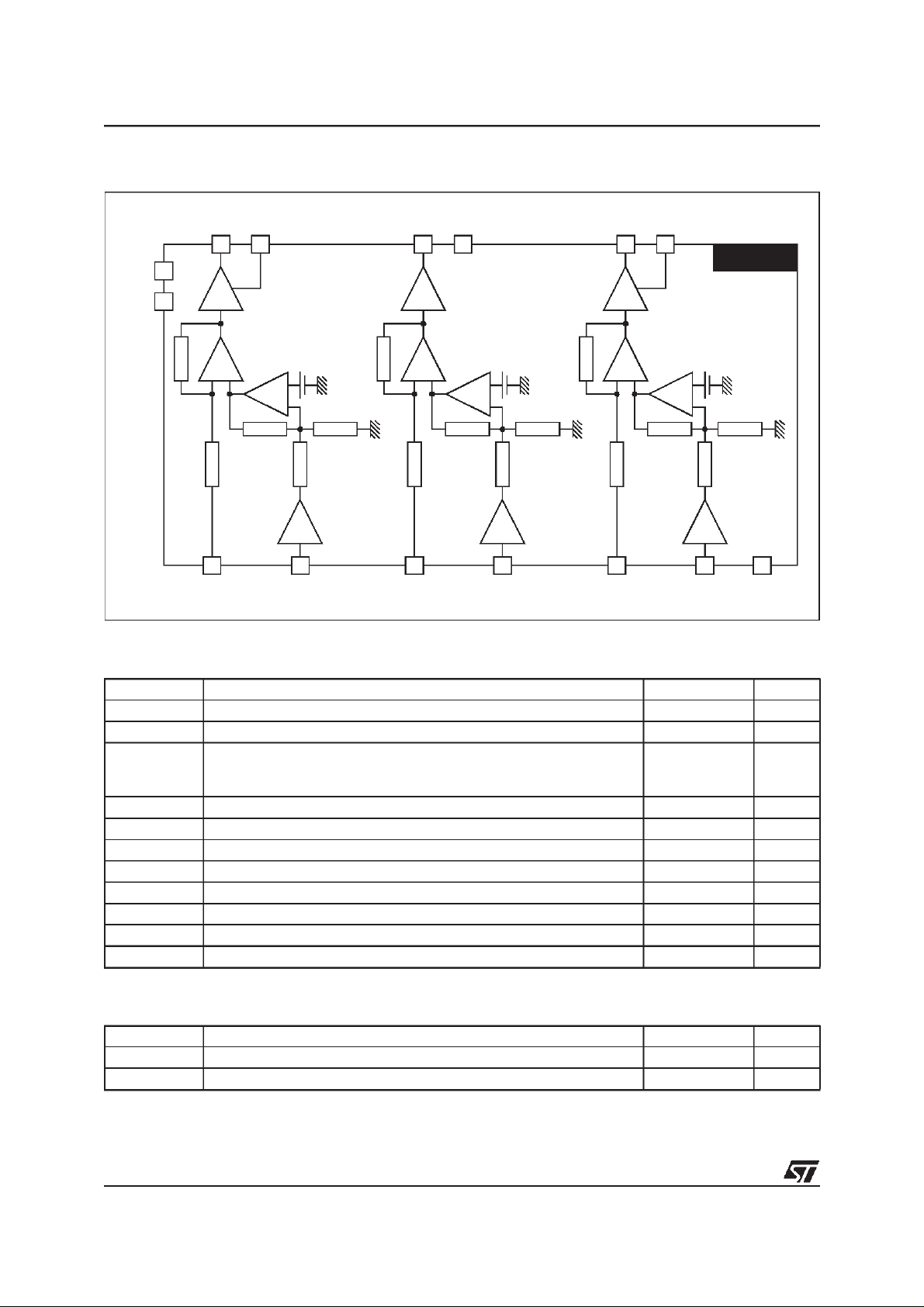
BLOCK DIAGRAM
1
3
V
DD
5
V
11
CC
42 106 12148
ABSOLUTE MAXIMUM RATINGS
GND2
OUT2GND1OUT1
OUT3
GND3
131597
TDA9533
GNDSC.OFF3IN3C.OFF2IN2C.OFF1IN1
Symbol Parameter Value Unit
V
DD
V
CC
High Supply Voltage 120 V
Low Supply Voltage 17 V
ESD Susceptibility
V
ESD
I
OD
I
OG
V
IMax
V
I Min
V
IC OFF Max
V
IC OFF Min
T
J
T
STG
Human Body Model, 100pF. Discharge through 1.5KΩ
EIAJ Norm, 200pF. Discharge through 0Ω
Output Source Current (pulsed < 50µs) 80 mA
Output Sink Current (pulsed < 50µs) 80 mA
Maximum Input Voltage 15 V
Minimum Input Voltage - 0.5 V
Maximum C. off Input Voltage VCC+ 0.5 V
Minimum C. off Input Voltage - 0.5 V
Junction Temperature 150 °C
Storage Temperature -20 + 150 °C
2
300
THERMAL DATA
Symbol Parameter Value Unit
R
R
th (j-c)
th (j-a)
Junction-Case Thermal Resistance (Max.) 3 °C/W
Junction-Ambient Thermal Resistance (Typ.) 35 °C/W
kV
V
2/8
TDA9533
ELECTRICAL CHARACTERISTICS
(VCC = 12V, VC OFF = 2.5V, VDD = 110V, Tamb = 25 °C, unless otherwise specified)
Symbol Parameter Test Conditions Min Typ Max Unit
V
DD
V
CC
I
DD
I
CC
/dV
dV
OUT
dV
OUT/dθ
d∆V
OUT/dθ
∆V
OUT
∆V
C.OFF
I
BC .OFF
V
OUT SATH
V
OUTSATL
AV
R
E
lin
OS Overshoot 5 %
Lf
∆g/g
R
IN
BW Bandwidth at -3dB
t
R,tF
t
SET
Lf CT
Hf CT
High Supply Voltage (Pin 5) 20 110 115 V
Low Supply Voltage (Pin 11) 10 12 15 V
High Voltage Supply Internal DC Cur-
rent
Low Voltage Supply Internal DC Current
High Voltage Supply Rejection V
DD
Output Voltage Drift Versus Temperature for any Channel
Differential Output Voltage Offset Drift
Versus Temperature
/
Cut-Off Control Gain
Cut-Off Control Bias Current V
Max. Output Voltage
Min. Output Voltage
Typical Video Gain V
Linearity Error 17<V
Low Frequency Gain Matching V
Video Input Resistor V
Rise and Fall Time
2.5% Settling Time
Low Frequency Crosstalk
High Frequency Crosstalk
V
= 50V
OUT
25
60
= 50V 0.5 %
OUT
= 80V 15
V
OUT
= 80V 5
V
OUT
= 80V
V
OUT
1V < V
OUT
<4V
C OFF
= 80V 10 µA
I0=-60mA, (1)
=60mA, (1)
I
0
= 50V 20
OUT
OUT<VDD
= 50V, f=1MHz 5 %
OUT
= 50V 2 KΩ
OUT
=50V,C
V
OUT
=200Ω, ∆V
R
P
V
=50V,C
OUT
=200Ω, ∆V
R
P
V
=50V,C
OUT
=200Ω, ∆V
R
P
=50V,C
V
OUT
=200 Ω,∆V
R
P
-15V 5 8 %
=8pF
LOAD
=20V
OUT
=8pF
LOAD
=40V
OUT
=8pF
LOAD
=40V
OUT
=8pF
LOAD
=20V
OUT
f=1MHz
f = 20MHz
14
V
DD
6.5
11
50 MHz
7.5 ns
15 ns
50
32
-
mA
mA
mV/
°C
mV/
°C
V
V
dB
dB
Note: 1
Pulsed current width < 50µs
3/8

TDA9533
TYPICAL APPLICATION
PC Board Lay-out
The best performance is obtained with a carefully
designed HF PC board, especially for the output
and input capacitors.
Rise/fall time and bandwidth are measured on
a 8pF load (including a PC board parasitical, socket and a CRT capacitor).
The input voltage range for the cut-off adjustment
pins is from 1 to 4 volts and a 10 nF to 47 nF bypass capacitor is recommended on these pins.
Power Dissipation
The power dissipation is the sum of the DC and
the dynamic dissipation.
As the feedback resistors are integrated, the DC
power dissipation (capacitive load) can be estimated by:
V
CC
V
CC
75Ω
TDA9533
P
STAT=VDD.IDD+VCC.ICC
The dynamic dissipation in worst case (full bandwidth and black pixel/white pixel picture - (2) is:
P
=3VDD.CL.V
DYN
OUT(PP)
.f.K
where f is the video frequency and K the active line
duration / total duration.
Example: for V
V
=40VPP,IDD= 25mA, I
OUT
f
We have: P
Therefore: P
Note: 2
V
= 40MHz, CL= 8pF and K = 0.72.
VIDEO
STAT
=6.51W.
tot
This worst thermal case must only be
considered for TJmax calculation.
Nevertheless, during the average life of the
circuit, the conditions are very close to the
white picture conditions.
DD 110V
V
DD
511
= 110V, V
DD
= 3.47W and P
GNDS
8
DYN
CC
= 60mA,
CC
= 3.04W
= 12V,
75
75Ω
V
C.OFF1
Ω
V
C.OFF2
V
C.OFF3
IN1
IN2
IN3
2
10
12
14
OUT1
R
4
C.OFF1
C.OFF2
6
C.OFF3
1
3
GND1
OUT2
7
9
GND2
OUT3
15
13
GND3
P
C
L
R
P
C
L
R
P
C
L
4/8

TDA9533
Figure 1. TDA9207/9209 - TDA9533/9530 Demonstration Board: Silk Screen and Trace (scale 1:1)
5/8

TDA9533
Figure 2. TDA9207/9209 - TDA9533/9530 Demonstration Board Schematic
F3(2)
D1(2)
5V
Jump
110V
C24 4.7uF /150V
R19(2)
33R
110V
SDA
SCL
2K7
2K7
123
4
J1
I2C
C1(1)
R3
2R7
R7 100R
Jump
S2
HSYNC
BLANK
R6
2R7
R5
2R7
R4
2R7
R9 33R
100nF
C4
D2
1N4148
5V
R12
4 4
E
D
R2
R1
5V
C
S1
5V5-8V
B
A
R11 150R/0.5W
FDH400
L1 .33uH
12V
R10 120R / 0.5W
transient response optimisation
Gout
OUT3
GND3
U2
IN3
C_OFF3
C3(1)
100nF
R13 100R
R14 15R/50R
100pF
C5(1) 100pF
21
22
23
24
BLK
R8 100R
U1
IN1
123456789
C2(1) 100nF
D3
1N4148
75R
Hs/BPCP
ABL
100nF
5V
R15 33R
C7
CUT1
IN2
D4
OUT1
GNDL
C9(1) 100nF
1N4148
110V
VCC
D6(2)
C11
C10(1)
C12(1)
GND2
IN2
R16 15R/50R
C8(1) 100nF
20
VCCP
IN3
D5
R17
FDH400
47uF
100nF
100nF/250V
OUT2
GNDS
R18 100R
18
19
OUT2
GNDA
C6(1) 100nF
1N4148
5V
75R
3 3
R22 150R / 0.5W
L2 .33uH
R21 120R/0.5W
Rout
VDD
C_OFF2
R20 15R/50R
17
GNDP
VCCA
D7
110V
GND1
C_OFF1
IN1
R24 100R
16
CUT2
OUT3
VDDL/AV
OSD1
R23 33R
100nF
C13
1N4148
D9(2)
123456789101112131415
OUT1
TDA9530/33
15
CUT3
OSD2
101112 13
D8
R25
FDH400
C15(1)
C14(1)
SDA
14
SDA
OSD3
Jump
S3
1N4148
75R
R27 150R / 0.5W
L3 .33uH
R26 120R / 0.5W
Bout
110V
100nF
100nF
SCL
FBLK SCL
AV
KB
C18
C17
100pF
C16
100pF
TDA9207/09
Jump
S4
OSD1
HEAT
101112
100nF/250V
J4
GND_CRT
Jump
S5
OSD2
F1(2)
C19
10nF/ 400V
9
H2
H1BGND
J3
10
R29
5V
1234567891011
J7
VFly
HFly AV
12
J6
Jump
S6
S7
FBLK
OSD3
2 2
KR
8
R
OSD1
OSD2
VSYNC
5-8V5VHSYNC
Jump
J5
OSD3
F2(2)
G2
7
G2
FBLK
SDA
Bin
C20
SCL
BLANK
HEATG1110V
in
Rin
10nF/ 2KV
G1 G
GND
HSYNC
HFly
HSYNC
VSYNC
G
KG
C25
56
1
VFly
12
OSD
12V
1234567891011
12
11
10
9
8
7
6
5
4
3
2
1
10nF/ 400V
150R
R28
G1
Supply
12V
5-8V
5V
J2 Video
<Doc>
CRT4TDA9207/09+TDA9533
A4
Title
Size DocumentNumber Rev
2: The purpose of all componentsfollowed by (2) is to ensure a
good protectionagainst overvoltage(arcing protection)
1: All capacitorsfollowed by (1) are decouplingcapacitors
which must be connected as close as possible to the device
Notes:
C23
47uF
C22
47uF
C21
47uF
1 1
11Monday,January 17,2000
Date: Sheet of
E
D
C
B
A
6/8

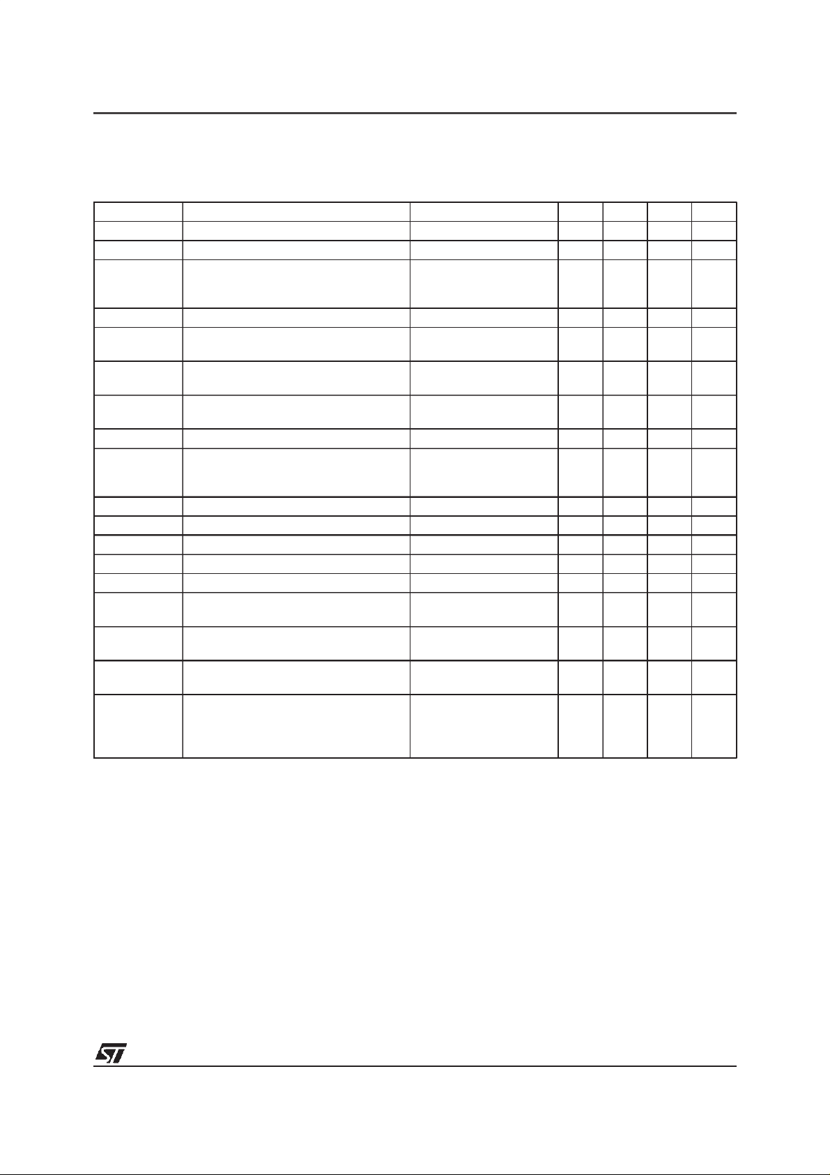
PACKAGE MECHANICAL DATA
15 PIN - PLASTIC MULTIWATT
TDA9533
A
C
L7
H1
S
S1
Dia 1
L3
L1
L2
L
L4
D
H2
B
E
MM1
Dimensions
A 5 0.197
B 2.65 0.104
C 1.6 0.063
D 1 0.039
E 0.49 0.55 0.019 0.022
F 0.66 0.75 0.026 0.030
G 1.02 1.27 1.52 0.040 0.050 0.060
G1 17.53 17.78 18.03 0.690 0.700 0.710
H1 19.6 0.772
H2 20.2 0.795
L 21.9 22.2 22.5 0.862 0.874 0.886
L1 21.7 22.1 22.5 0.854 0.870 0.886
L2 17.65 18.1 0.695 0.713
L3 17.25 17.5 17.75 0.679 0.689 0.699
L4 10.3 10.7 10.9 0.406 0.421 0.429
L7 2.65 2.9 0.104 0.114
M 4.25 4.55 4.85 0.167 0.179 0.191
M1 4.63 5.08 5.53 0.182 0.200 0.218
S 1.9 2.6 0.075 0.102
S1 1.9 2.6 0.075 0.102
Dia. 1 3.65 3.85 0.144 0.152
Min. Typ. Max. Min. Typ. Max.
Millimeters Inches
F
G1
G
7/8

TDA9533
Information furnished is believed to be accurate and reliable. However, STMicroelectronics assumes no
responsibility for the consequences of use of such information nor for any infringement of patents or other
rights ofthird parties which may result from its use. No license is granted by implication orotherwise underany
patent orpatent rights of STMicroelectronics. Specifications mentioned in this publication are subject tochange
without notice. This publication supersedes and replaces all information previously supplied.
STMicroelectronics products are not authorized for use as critical components in life support devices or
systems without express written approval of STMicroelectronics.
The ST logo is a trademark of STMicroelectronics.
2000 STMicroelectronics - All Rights Reserved
Purchase of I
Rights to use these components in a I
2
C Components ofSTMicroelectronics, conveys a license under the PhilipsI2C Patent.
2
C system, is granted provided that the system conforms to the I2C
Standard Specifications as defined by Philips.
STMicroelectronics GROUP OF COMPANIES
Australia - Brazil - China - Finland -France -Germany - Italy - Japan - Korea - Malaysia - Malta - Mexico -Morocco - The
Netherlands - Singapore - Spain - Sweden - Switzerland - Taiwan - Thailand - United Kingdom - U.S.A.
http://www.st.com
8/8
 Loading...