

DC COUPLINGHIGH VOLTAGE VIDEO AMPLIFIER
.
BANDWIDTH : 40MHzTYPICAL
.
RISEANDFALLTIME : 9nsTYPICAL
.
SUPPLYVOLTAGE: 110V
.
POWERDISSIPATION: 3.0W
.
ESD PROTECTED
DESCRIPTION
The TDA9511isa video amplifier designed with a
high voltage Bipolar/CMOS/DMOS technology
(BCD).It drives in DC coupling modeone cathode
of a monitor and is protected against flashovers.
It is available in Heptawatt package.
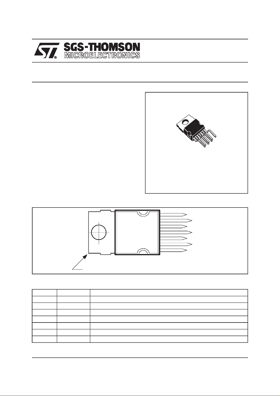
HEPTAWATT
(Plastic Package)
ORDER CODE :
TDA9511
TDA9511
PIN CONNECTIONS
7
6
5
4
3
2
1
Tab connected to Pin 4
PIN CONFIGURATION
Pin N Symbol Function
1 IN- Inputof the amplifier
2V
3V
4 GNDA Analog Ground
5 GNDP Power Ground
6 OUT Output driving the cathode
7V
CC
REF
DD
Low VoltagePower Supply(12V Typ.)
Internal Voltage Reference (3.3V)
High Voltage Power Supply (110V Max.)
V
DD
OUT
GNDP
GNDA
V
REF
V
CC
IN-
9511-01.EPS
9511-01.TBL
April 1998
1/5
TDA9511
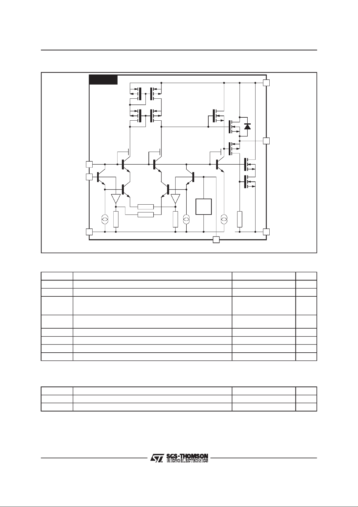
BLOCKDIAGRAM
CC
IN- 1
TDA9511
2V
4AGND
V
7
DD
6 OUT
V
REF
5 PGND
3
V
REF
9511-02.EPS
ABSOLUTE MAXIMUMRATINGS
Symbol Parameter Value Unit
V
DD
V
CC
Supply High Voltage (Pin 7) 120 V
Supply Low Voltage (Pin 2) 20 V
VESD ESD Susceptibility
I
OD
I
OG
I
j
T
j
T
oper
T
stg
Note 1 :
Pulsed current t≤50µs
Human Body Model, 100pF Discharge through 1.5kΩ
EIAJ Norm, 200pF Discharge through 0Ω
Output Current to VDD(Pin 6)
Output Current to Ground (Pin 6) (see Note 1)
Input Current (Pin 1) 50 mA
Junction Temperature 150
Operating Ambient Temperature 0, +70
Storage Temperature -20, +150
2
300
protected
80 mA
THERMAL DATA
Symbol Parameter Value Unit
R
R
th (j-c)
th (j-a)
Junction-Case Thermal Resistance Max. 3
Junction-Ambient Thermal Resistance Typ. 70
kV
o
o
o
o
C/W
o
C/W
V
C
C
C
9511-02.TBL
9511-03.TBL
2/5

TDA9511
ELECTRICAL CHARACTERISTICS
= 12V,VDD= 110V,T
(V
CC
=25oC, unless otherwisespecified)
amb
Symbol Parameter Test Conditions Min. Typ. Max. Unit
V
V
I
I
V
V
dV
IN
dV
IN
V
SATH
V
SATL
ELin Linearity Error 17V < V
High Supply Voltage(Pin 7) 20 110 V
DD
Low SupplyVoltage (Pin 2) 10 12 15 V
CC
DCCurrentofHighVoltageSupply
DD
(without feedback current)
Low VoltageSupply Internal DC Current 15 mA
CC
Internal Reference (Pin 3) 3.2 V
REF
Input Voltage V
IN
/dVCCDrift of Input Voltage versus V
CC
V
= 60V 9 mA
OUT
= 60V 3.25 V
OUT
Measured on Pin 1 0.12 %
/dT Driftof InputVoltageversus Temperature 0.5 mV/oC
High OutputSaturation Voltage (Pin 6) IO= -60mA VDD- 8.5 V
Low OutputSaturationVoltage (Pin 6) IO= 60mA 12 V
OUT<VDD
- 15V 5 %
OS Overshoot 5%
BW Bandwidth at -3dB Measured on CRT cathodes.
= 10pF, Rprotect = 220Ω,
C
LOAD
t
R,tF
G
Rise and Fall Time Measured between 10% & 90%
Open Loop Gain V
O
= 60V, ∆V
V
OUT
Feedback gain= 20
of output pulse,
= 10pF, Rprotect = 220Ω,
C
LOAD
= 60V, ∆V
V
OUT
= 60V 60 dB
OUT
OUT
OUT
= 20VPP,
= 40V
PP
Open Loop Gain Temperature
40 MHz
9ns
o
0.03 dB/
C
Coefficient
I
R
Note 2 : Characterized and not tested.
Input Bias Current(Pin 1) V
IB
= 60V 20 30 µA
OUT
Input Bias TemperatureCoefficient 90 nA/
Input Resistance See Note 2 200 kΩ
IN
o
C
9511-04.TBL
Figure1 : Measurementof Input Voltage
V
VIN=
OUT
(1 + R2/R1)
R1
R2
V
IN
V
OUT
9511-03.EPS
3/5

TDA9511
TYPICALAPPLICATION
TheTDA9511consists of :
- A differentialamplifierwithactiveload,
- A DMOS output buffer,
- Abandgapvoltagereference(Pin3forfilteringonly).
PC boardlay-out
The best performances are obtained with a carefully designed HF PC-Board, especially for the
output and input capacitors.
ThefeedbackresistorR
capacitor(C
< 0.3pF).
F
This parasitic capacitor C
by a capacitor R3 (roughly 20 ⋅ C
parallelwiththe input resistor R1.
The full bandwidth of the device is only obtained
with well matched compensation otherwise the
applicationwill have either an integrator response
with a low bandwidth or a differentiator response
withtoo much ringing.
Adiode D
(seeFigure2) has to be connectedfor
P
flashoverprotection.
Figure2 :
TypicalEvaluationSchematic
musthavea lowparasitic
F
must be compensated
F
) connected in
F
Powerdissipation
The power dissipationconsistsof a staticpart and
a dynamic part. The static dissipation varies with
the output voltage and the feedbackresistor. The
dynamicpower dissipationincreaseswiththepixel
frequency.
Fora signalfrequencyof40MHzand40V
PP
output
signal,thetypicalpower dissipationisabout3.0W,
DD
=110V.
for V
In firstapproximation,the dynamicdissipation is :
P
D=VDD*CLOAD
* ∆V
OUT
*f
and the total dissipation is :
P=V
DD*CLOAD
*∆V
+VCC*ICC-(VDD-V
*f+VDD*I
OUT
_____
)
OUT
_____
V
OUT
R
FEEDBACK
DD
with f = pixel frequency
P = 110Vx 10pF x 40V x 40MHz + 110Vx 7mA
+12 x 20mA- 60
2
V/20kΩ= 2.95W
IN
R1
R3
C3
V
IN
Recommendedvalues :
R1 = 1kΩ, R2 = 1.8kΩ,R
=20kΩ,RP= 200Ω,
F
C4 > 10nF, C3 = 10 to 12pFfor C
R3 # 150Ω.
R2
F
# 0.5pF.
C4
C
F
R
F
V
1
3
V
CC
2
DD
D
P
OUT
R
P
C
V
OUT
LOAD
t
9511-04.EPS
7
6
5
4
V
4/5

TDA9511
PACKAGEMECHANICAL DATA :
Dimensions
Min. Typ. Max. Min. Typ. Max.
7 PINS - PLASTICHEPTAWATT
Millimeters Inches
A 4.8 0.189
C 1.37 0.054
D 2.4 2.8 0.094 0.110
D1 1.2 1.35 0.047 0.053
E 0.35 0.55 0.014 0.022
F 0.6 08 0.024 0.031
F1 0.9 0.035
G 2.41 2.54 2.67 0.095 0.100 0.105
G1 4.91 5.08 5.21 0.193 0.200 0.205
G2 7.49 7.62 7.8 0.295 0.300 0.307
H2 10.4 0.409
H3 10.05 10.4 0.396 0.409
L 16.97 0.668
L1 14.92 0.587
L2 21.54 0.848
L3 22.62 0.891
L5 2.6 3 0.102 0.118
L6 15.1 15.8 0.594 0.622
L7 6 6.6 0.236 0.260
M 2.8 0.110
M1 5.08 0.200
Dia. 3.65 3.85 0.144 0.152
Informationfurnished is believed to be accurate and reliable.However,SGS-THOMSONMicroelectronics assumesno responsibility
for the consequences of use of such information nor for any infringement of patentsor other rights of third parties which may result
from itsuse.No licence is grantedby implication orotherwise underany patent or patent rights of SGS-THOMSONMicroelectronics.
Specifications mentioned in this publication are subject to change without notice. This publication supersedes and replaces all
informationpreviouslysupplied. SGS-THOMSON Microelectronics products are notauthorized for useas criticalcomponents in life
support devices or systems without express written approval of SGS-THOMSON Microelectronics.
PM-HEPTV.EPS
HEPTV.TBL
1998 SGS-THOMSON Microelectronics - AllRights Reserved
Purchase of I
2
C Patent. Rights to use these components in a I2C system, is granted provided that the system conforms to
I
Australia - Brazil - Canada- China - France- Germany - Italy - Japan - Korea - Malaysia - Malta- Morocco
The Netherlands - Singapore - Spain - Sweden- Switzerland - Taiwan - Thailand - United Kingdom - U.S.A.
2
C Components of SGS-THOMSON Microelectronics, conveys a license under the Philips
2
the I
C Standard Specifications as defined by Philips.
SGS-THOMSON Microelectronics GROUP OF COMPANIES
5/5
 Loading...