

VERTICALDEFLECTION BOOSTER
.
POWERAMPLIFIER
.
FLYBACKGENERATOR
.
THERMAL PROTECTION
.
OUTPUTCURRENT UP TO 2.0A
.
FLYBACKVOLTAGEUP TO 70V (on Pin5)
.
SUITABLEFOR DC COUPLING APPLICATION
DESCRIPTION
Designedfor monitors andhighperformance TVs,
the TDA9309 vertical deflection booster delivers
flyback voltagesupto 70V.
TheTDA9309operateswithsuppliesupto35Vand
provides up to 2App output current to drive the
yoke.
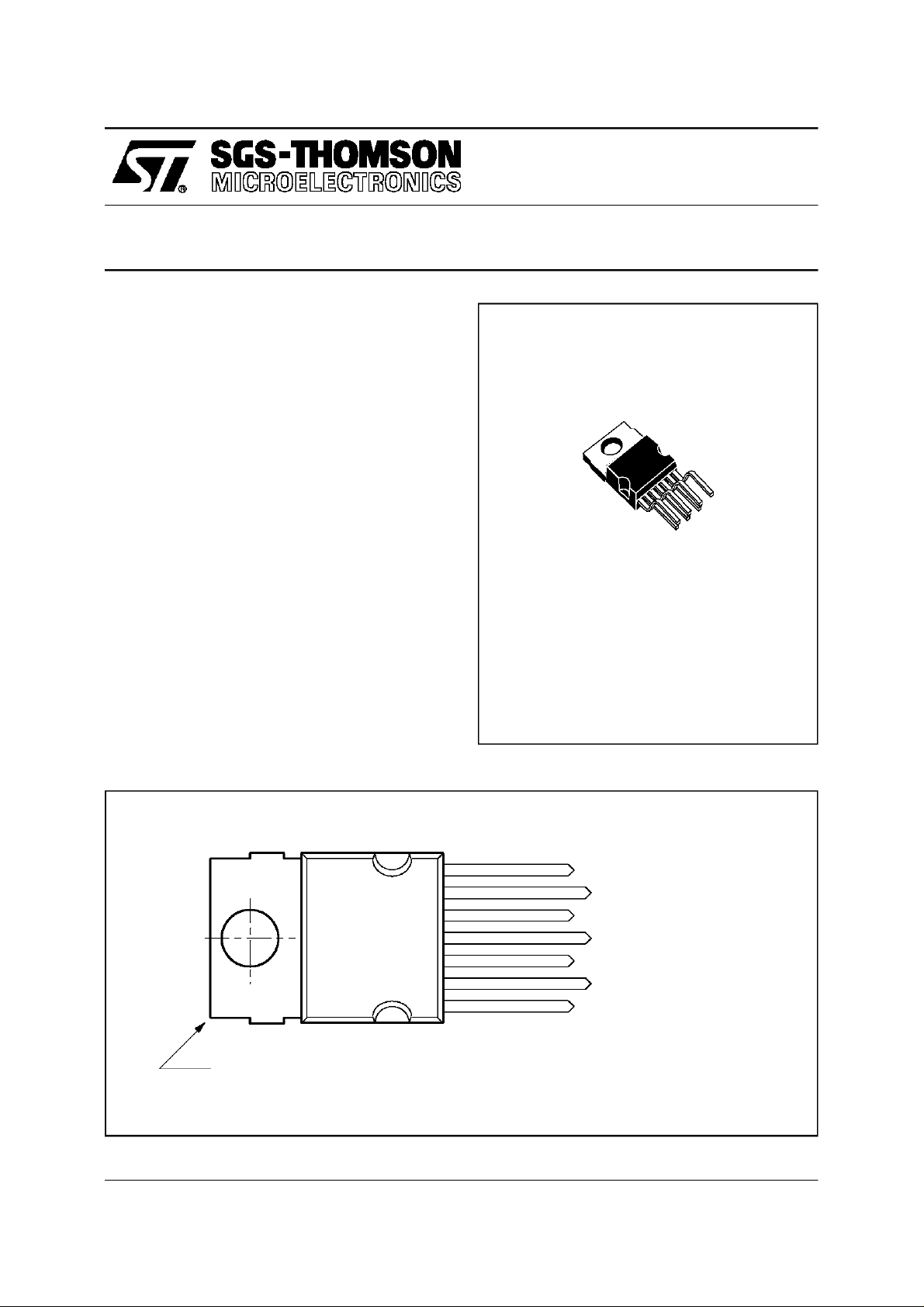
The TDA9309is offeredinHEPTAWATTpackage.
PP
TDA9309
HEPTAWATT
(Plastic Package)
ORDER CODE : TDA9309
PIN CONNECTIONS
Tab conne cted to pin 4
November 1996
7
6
5
4
3
2
1
Inverting Input
Output S tage Supply
Outp u t
GND
Flyback Generator
Supply V oltage
Non-inverting Input
9309-01.EPS
1/6
TDA9309
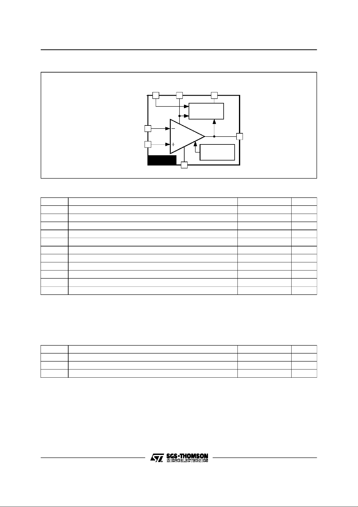
BLOCK DIAGRAM
OUTPUT
SUPPLY
VOLTAGE
STAGE
SUPPLY
236
FLYBACK
GENERATOR
FLYBACK
GENERATOR
INVERTING INPUT
NON-INVERTING INPUT
7
1
TDA9309
POWER
AMPLIFIER
4
GROUND
THERMAL
PROTECTION
5
OUTPUT
ABSOLUTEMAXIMUM RATINGS
Symbol Parameter Value Unit
V
V
V
1,V7
V
I
I
I
V
ESD
T
oper
T
T
Notes : 1. Versus Pin 4.
Supply Voltage (Pin 2)(see note1) 40 V
S
Flyback PeakVoltage(Pin 6)(see note1) 70 V
6
Amplifier Input Voltage(Pins 1-7) (see note 1) V
Voltageat Pin 3(see note5) VS+ 3.0 V
3
Maximum OutputPeak Current (see notes 2 and 3) 1.5 A
O
Maximum SinkCurrent (first part of flyback) (t < 1ms) 1.5 A
3
Maximum SourceCurrent (t < 1ms) (see note 2) 1.5 A
3
S
Electrostatic Handling for all pins (see note 4) 2000/300 V
Operating Ambient Temperature - 20, + 75
Storage Temperature - 40, + 150
stg
Junction Temperature +150
j
2. The output current can reach 4Apeak for t ≤ 10µs (up to 200Hz).
3. Provided SOAR is respected (see Figures1 and 2).
4. Equivalent to discharging a 100pF capacitor through a 1.5kΩ serial resistor / 200pF capacitor through0Ω resistor.
5. This will occurduring 1sthalf of flyback pulse.
9309-02.EPS
V
o
C
o
C
o
C
9309-01.TBL
THERMALDATA
Symbol Parameter Value Unit
Junction-case Thermal Resistance Max. 3
Temperature for Thermal Shutdown 150
t
Recommended Max. JunctionTemperature 120
jr
2/6
R
th (j-c)
T
T
o
C/W
o
C
o
C
9309-02.TBL

TDA9309
ELECTRICAL CHARACTERISTICS
= 35V, TA=25oC, unless otherwisespecified)
(V
S
Symbol Parameter Test Conditions Min. Typ. Max. Unit
V
V
∆V
GV VoltageGain 80 dB
V
V
V
D5 - 6
V
D3 - 2
V
V
Operating Supply VoltageRange 10 35 V
S
Pin 2 Quiescent Current I3=0,I5=0 9 20 mA
I
2
Pin 6 Quiescent Current I3=0,I5=0,V6= 35V 8 19 35 mA
I
6
Max. Peak Output Current ±1A
I
O
Amplifier Bias Current V1=1V,V7= 2.2V - 0.6 - 1.5 µA
I
1
Amplifier Bias Current V1= 2.2V,V7= 1V - 0.6 - 1.5 µA
I
7
Offset Voltage 3 mV
IO
/dt Offset Driftversus Temperature - 10 µV/oC
IO
Output Saturation Voltage to GND (Pin 4) I5= 1A 1 1.7 V
5L
Output Saturation Voltage to Supply (Pin 6) I5= - 1A 1.8 2.3 V
5H
Diode Forward Voltagebetween Pins 5-6 I5= 1A 1.3 2 V
Diode Forward Voltagebetween Pins 3-2 I3= 1A 1.2 2 V
Saturation Voltage on Pin 3 I3= 20mA 0.4 1 V
3SL
Saturation Voltage to Pin 2 (2nd part of flyback) I3= - 1A 2.1 2.8 V
3SH
9309-03.TBL
APPLICATION CIRCUITS
AC COUPLING
V
REF
2.2V
R5
+V
C
F
236
FLYBACK
GENERATOR
7
1
POWER
AMPLIFIER
THERMAL
PROTECTION
TDA9309
4
R3
R2
S
5
Ω
1.5
330Ω
YOKE
0.22µF
R4
C
R1
L
3/6
9309-03.EPS

TDA9309
APPLICATION CIRCUITS(continued)
DC COUPLING
236
R3
7
V
REF
V
REF
Vertical
Position
Adjustment
1
TDA9309
POWER
AMPLIFIER
V
EE
C
F
FLYBACK
GENERATOR
4
+V
S
THERMAL
PROTECTION
5
Ω
1.5
330Ω
YOKE
0.22µF
R2
Figure1 : Output TransistorsSOA
Figure2 : SecondaryBreakdownTemperature
(forsecondarybreakdown)
I(A)
C
10
@T
case
=25 C
1
-1
10
t=1ms
t =10ms
V (V)
CE
10
-2
t=100ms
11010
100
2
9309-05.EPS
R1
Derating Curve
(ISB = secondarybreakdowncurrent)
ISB (%)
90
80
70
T
(°C)
case
60
25 50 75 100 125
9309-04.EPS
9309-06.EPS
4/6

PIN CONFIGURATION
Figure 3 : Pins1-7
V
S
17
Figure4 : Pin 3
V
S
3
TDA9309
Figure 5 : Pins5-6
9309-07.EPS
6
9309-08.EPS
V
S
5
9309-09.EPS
5/6

TDA9309
PACKAGE MECHANICAL DATA : HEPTAWATT
Dimensions
Min. Typ. Max. Min. Typ. Max.
A 4.8 0.189
C 1.37 0.054
D 2.4 2.8 0.094 0.110
D1 1.2 1.35 0.047 0.053
E 0.35 0.55 0.014 0.022
F 0.6 08 0.024 0.031
F1 0.9 0.035
G 2.41 2.54 2.67 0.095 0.100 0.105
G1 4.91 5.08 5.21 0.193 0.200 0.205
G2 7.49 7.62 7.8 0.295 0.300 0.307
H2 10.4 0.409
H3 10.05 10.4 0.396 0.409
L 16.97 0.668
L1 14.92 0.587
L2 21.54 0.848
L3 22.62 0.891
L5 2.6 3 0.102 0.118
L6 15.1 15.8 0.594 0.622
L7 6 6.6 0.236 0.260
M 2.8 0.110
M1 5.08 0.200
Dia. 3.65 3.85 0.144 0.152
Millimeters Inches
PM-HEPTV.EPS
HEPTV.TBL
Information furnishedis believed to be accurate andreliable. However, SGS-THOMSON Microelectronics assumes no responsibility
for the consequences ofuse ofsuch information nor forany infringement ofpatents or other rights of third parties which may result
from its use. No licence is granted byimplication or otherwise under any patent or patent rightsof SGS-THOMSONMicroelectronics.
Specifications mentioned in this publication are subject to change without notice. This publication supersedes and replaces all
information previously supplied.SGS-THOMSON Microelectronicsproducts are not authorized for use as critical components in life
support devices or systems withoutexpress written approval of SGS-THOMSON Microelectronics.
1996 SGS-THOMSON Microelectronics - All Rights Reserved
Purchase of I2C Components of SGS-THOMSON Microelectronics, conveys a license under the Philips
2
I
C Patent. Rights to use these components in a I2C system, is granted provided that the system conformsto
Australia - Brazil -Canada -China -France - Germany - Hong Kong - Italy - Japan - Korea - Malaysia - Malta - Morocco
The Netherlands - Singapore - Spain - Sweden - Switzerland - Taiwan - Thailand - United Kingdom -U.S.A.
2
the I
C Standard Specifications as defined by Philips.
SGS-THOMSON Microelectronics GROUP OF COMPANIES
6/6
 Loading...