

150 MHz PIXEL VIDEO CONTROLLER FOR MONITORS
FEATURE
■ 150 MHZ PIXEL RATE
■ 2.7 ns RISE ANDFALL TIME
2
■ I
C BUS CONTROLLED
■ GREY SCALE TRACKING VERSUS BRIGHT-
NESS
■ OSD MIXING
■ NEGATIVE FEED-BACK FOR DC COUPLING
APPLICATION
■ INTERNAL POSITIVE FEED-BACK FOR LCD
APPLICATION
■ 0.5~4.5 V DACs FOR BLACK LEVEL RESTO-
RATION (AC-COUPLING APPLICATION) OR
CUT-OFF CONTROLS (FOR DC-COUPLING
APPLICATION USING THE ST AMPLIFIERS
TDA9533/9530)
■ BEAM CURRENT ATTENUATION (ABL)
■ PEDESTRAL CLAMPING ON OUTPUT
STAGE
■ POSSIBILITY OF LIGHT OR DARK GREY
OSD BACKGROUND
■ OSD INDEPENDENT CONTRAST CONTROL
■ ADJUSTABLE BANDWIDTH
■ INPUT BLACK LEVEL CLAMPING WITH
BUILT-IN CLAMPING PULSE
■ STAND-BY MODE
■ 5 V TO 8 V POWER SUPPLY
■ SYNC CLIPPING FUNCTION (SOG)
DESCRIPTION
The TDA9207 is an I2C Bus controlled RGB preamplifier designed for Monitor application, able to
mix the RGB signals coming from any OSD device. The usual Contrast, Brightness, Drive and
Cut-Off Controls are provided.
In addition, it includes the following features:
– OSD contrast,
– Bandwidth adjustment,
– Grey background,
– Internal back porchclamping pulse generator.
TDA9207
INCLUDING CUT-OFF INPUTS
SHRINK DIP24
(Shrink Plastic Package)
ORDER CODE: TDA9207
The RGB incoming signals are amplified and
shaped todrive any commonlyused videoamplifiers without intermediate follower stages. Even
though encapsulated in a 24-pin package only,
this IC allows any kind of CRT Cathode coupling :
– AC coupling with DC restore,
– DC coupling with Feed-back from Cathodes,
– DC coupling with Cut-Off controls of the Video
amplifier (ST Amplifiers TDA9533/9530).
As forany STVideo pre-amplifier, theTDA9207 is
able to drive a real load without any external interface.
One of the main advantages of ST devices is their
ability to sink and source currents while most of
the devices from our competitors have problems
to sink largecurrents.
These driving capabilities combined with an original outputstage structuresuppress any static current on the output pins and therefore reduce dramatically the power dissipation of the device.
Extensive integrationcombined with high performance and advanced features make the TDA9207
one of the best choice for any CRT Monitor in the
14” to 17” range.
Perfectly matched with the ST Video Amplifiers
TDA9530/33, these 2 products offer a complete
solution for high performance and cost-optimized
Video Board Application.
Version 4.2
March 2000 1/22
1
TDA9207
1 -PIN CONNECTIONS
IN1
ABL
IN2
GNDL
IN3
GNDA
V
CCA
NC
OSD1
OSD2
OSD3
FBLK
1
2
3
4
5
6
7
8
9
10
11
12
24
23
22
21
20
19
18
17
16
15
14
13
BLK
HSYNC or BPCP
CO1/FB1
OUT1
V
CCP
OUT2
GNDP
OUT3
CO3/FB3
CO2/FB2
SDA
SCL
2 -PIN DESCRIPTION
Pin Number Symbol Description
1 IN1 Red Video Input
2 ABL ABL Input
3 IN2 Green Video Input
4 GNDL Logic Ground
5 IN3 Blue Video Input
6 GNDA Analog Ground
7V
8 NC Not Connected
9 OSD1 Red OSD Input
10 OSD2 Green OSD Input
11 OSD3 Blue OSD Input
12 FBLK Fast Blanking
13 SCL SCL
14 SDA SDA
15 CO2/FB2 Green Cut-off Output/Feedback Input
16 CO3/FB3 Blue Cut-off Output/Feedback Input
17 OUT3 Blue Video Output
18 GNDP Power Ground
19 OUT2 Green Video Output
20 V
21 OUT1 Red Video Output
22 CO1/FB1 Red Cut-off Output/Feedback Input
23 HSYNC
24 BLK Blanking Input
CCA
CCP
BPCP
Analog VCC(5V)
Power VCC(5 V to 8 V)
HSYNC
BPCP
2/22

3 - BLOCK DIAGRAM
TDA9207
V
REF
1
IN1
Clamp
IN2
3
IN3
5
ABL
GNDL
GNDA
VCCA
NC
2
BPCP
4
6
7
8
23 14 13 9 10 11
HSYNC SDA SCL
or BPCP
Contrast/8bit
Latches
Decoder
BLK FBLK VCCP
2
I
C
Bus
24
Contrast
D/A
OSD
Cont.
4bits
12
Output Clamp Pulse
(OCL)
Drive
Green Channel
Blue Channel
Brightness
8bits
OSD1 OSD2 OSD3
Drive
3x8bits
I C
Cut-off
8bits
20
Output
Stage
V
Output
DC Level
REF
4bits
TDA9207
OUT1
21
CO1/FB1
22
OUT2
19
CO2/FB2
15
OUT3
17
CO3/FB3
16
GNDP
18
See Figure 12 for complete BP CP and OCL generation diagram
4 - FUNCTIONAL DESCRIPTION
4.1 RGB Input
The three RGBinputs have to be supplied through
coupling capacitors (100 nF).
The maximum input peak-to-peak video amplitude
is 1 V.
The input stage includes a clamping function. The
clamp uses the input serial capacitor as a”memory capacitor”.
To avoid a discharge of the serial capacitor during
the line (due to leakage current), the input voltage
is referenced to the ground.
The clamp is gated by an internally generated
”Back Porch Clamping Pulse” (BPCP). Register 8
allows to choose the way to generate this BPCP
(see Figure 1).
When bit 0 is set to 0, the BPCP is synchronized
on the trailing or leading edge of HSYNC (Pin 23)
(bit 1 =0: trailing edge, bit 1 = 1: leading edge).
3/22
TDA9207
Additionally, the IC automatically works with either
positive or negative HSYNC pulses.
– When bit 0 is set to 1,BPCP is synchronized on
the leading edge of the blanking pulse BLK
(Pin 24).One can use a positive or negative
blanking pulse by programming bit 0 in
Register 9 (See I2C Table 3).
– BPCPwidth can be adjusted with bit2 and3 (see
Register 8, I2C table 2).
– If the application already provides the Back
Porch Clamping Pulse, bit 4 must be set to 1
(providing a direct connection between Pin 23
and internal BPCP).
4.2 Synchro Clipping Function
This function is available on channel 2 (Green
Channel). When using the Sync On Green (SOG)
(Synchro pulse included in the green channel in-
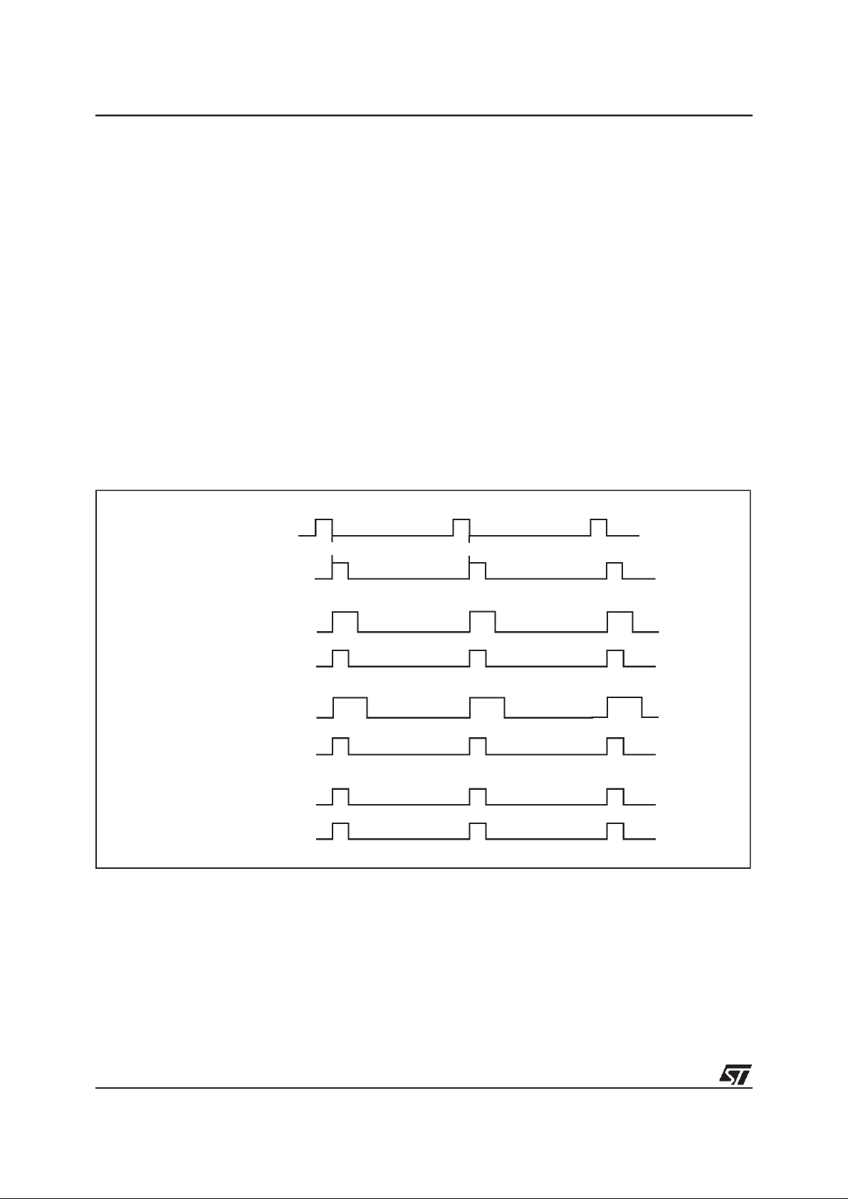
Figure 1.
R8b0=0 and R8b1=0
HSYNC/BPCP (Pin23)
Internal BPCP
put) the synchro clipping function must be activated (bit 7 set to 1 in register 9) in order to keep the
right green output levels and avoid unbalanced
colours.
4.3 Blanking Input
The Blanking pin (FBLK) isTTL compatible.
The Blanking pulse can be:
– positive or negative
– line or Composite-type (but not Frame-type).
4.4 Contrast Adjustment (8 bits)
The contrast adjustment is made bycontrolling simultaneously the gain ofthe three internal amplifiers through the I2C bus interface. Register 1 allows the adjustment in arange of 48 dB.
R8b0=0 and R8b1=1
HSYNC/BPCP (Pin23)
Internal BPCP
R8b0=1
R8b4 =1
HSYNC/BPCP (Pin23)
BLK (Pin24)
Internal BPCP
Internal BPCP
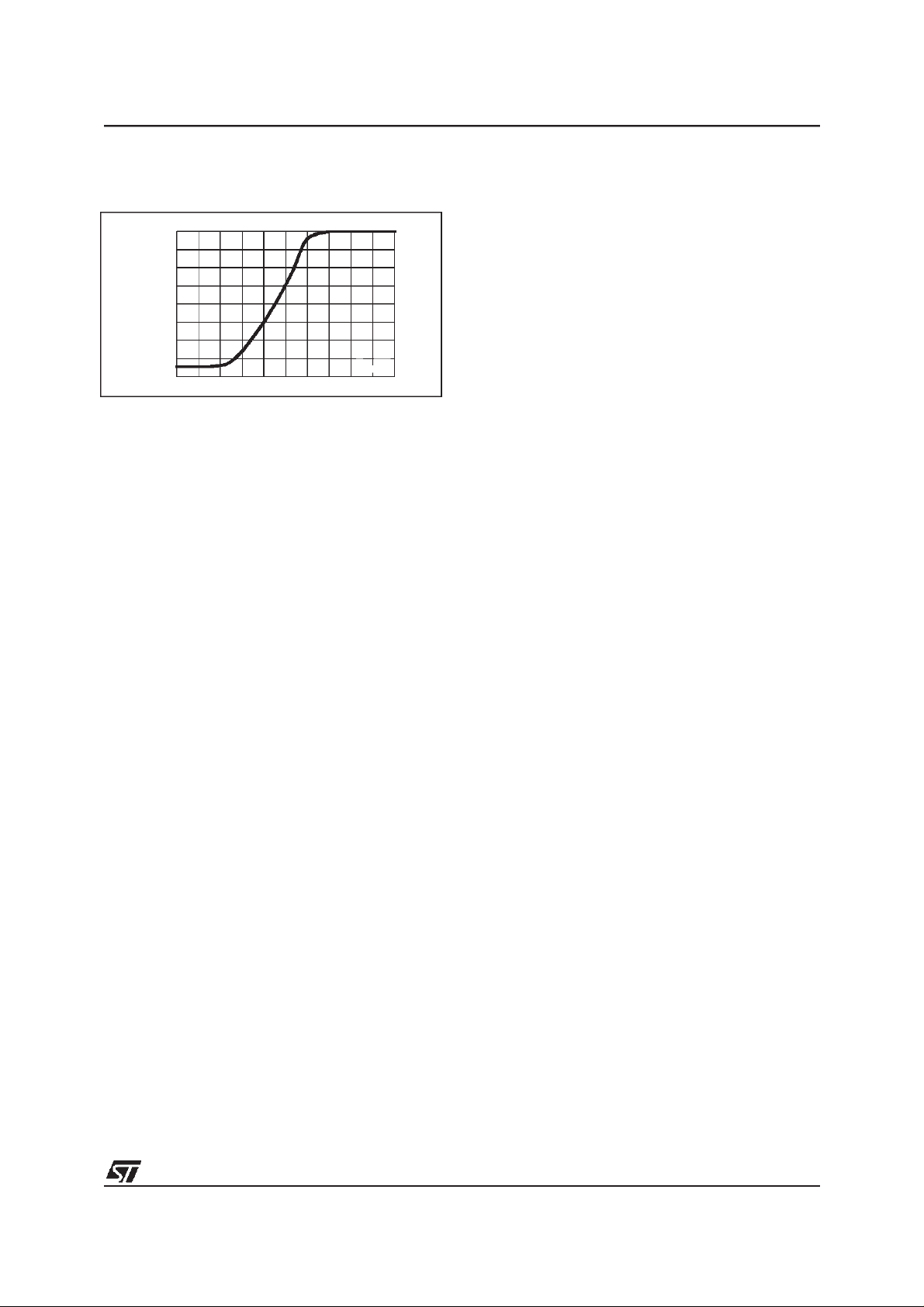
4.5 ABL Control
The TDA9207 includes an ABL (automatic beam
limitation) input to attenuate the RGB Video signals depending on the beam intensity.
The operating rangeis 2 V (from3 V to1 V). A typical 15 dB maximum attenuation is applied to the
output signal whatever the contrast adjustment is.
(See Figure 2 ).
When the ABL feature is not used, the ABL input
(Pin 2) must be connectedto a5V supplyvoltage.
4/22
TDA9207
Figure 2.
Attenuation (dB)
0
-2
-4
-6
-8
-10
-12
-14
-16
0
(V)
V
ABL
4321
5
4.6 Brightness Adjustment (8 bits)
Brightness adjustment is controlled by the I2C Bus
via Register 2. It consists of adding the same DC
voltage to the three RGBsignals,after contrast adjustment. When the blanking pulse equals 0, the
DC voltageis set toa value whichcan be adjusted
between 0 and 2V with 8mVsteps (see Figure 3).
The DC output level is forced to the ”Infra Black”
level (VDC) when the blanking pulseis equal to 1.
4.7 Drive Adjustment (3 x 8 bits)
In order to adjust the white balance,the TDA9207
offers the possibility of adjusting separately the
overall gain ofeach channel thanks to the I2C bus
(Registers 3, 4 and 5).
The very large drive adjustment range (48 dB) allows different standards or custom color temperatures.
It can also be usedto adjust the output voltages at
the optimum amplitude to drive the CRT drivers,
keeping the whole contrast control for the enduser only.
The drive adjustment is located after the Contrast,
Brightness and OSD switch blocks, so it does not
affect the white balance setting when the BRT is
adjusted. It also operates on the OSD portion of
the signal.
4.8 OSD Inputs
The TDA9207 allows to mix the OSD signals into
the RGB main picture. The four pins dedicated to
this function are the following:
– Three TTL RGB inputs (Pins 9, 10,11) connect-
edtothethree outputs ofthe corresponding OSD
processor.
– One TTL fast blanking input (Pin 12) also con-
nected tothe FBLK output ofthe OSD processor.
When a high level is present on the FBLK, the IC
acts as follows:
– The three main picture RGB input signals (IN1,
IN2, IN3) are internally switched to the internal
input clamp reference voltage.
– The three outputsignals are setto the voltage
corresponding to the three OSD input logic
states (0 or 1). (See Figure 3).
If the OSD input is at low level, the output and
brightness voltages (V
) are equal.
BRT
If the OSD input is at high level,the output voltage
is V
an I2C bus-controlled voltage.
, where V
OSD
OSD=VBRT
+ OSD and OSD is
OSD variesbetween0 V to 4.9 V by 320 mV steps
via Register 7 (4 bits). The same variation is applied simultaneously to the three channels providing the OSD contrast.
The grey color can be obtained on output signals
when:
– OSD1 = 1, OSD2 = 0 and OSD3 = 1,
– A special bit(bit 5 or 6) in Register 9 is set to 1.
If R9b5 is set to 1, light grey is obtained on output.
If R9b6is setto 1, dark grey is obtained on output.
In thecase where R9b5 and R9b6are setto 0, the
normal operation is provided on output signals.
4.9 Output Stage
The overall waveforms of the output signal are
shown in Figure 3 and Figure 4. The three output
stages, which are large bandwidth output amplifiers, areabletodeliver up to 4.4VPPfor0.7VPPon
input.
When a high level is applied on the BLK input
(Pin 24), the three outputs are forced to ”Infra
Black” level(VDC) thanks to a sample and holdcircuit (described below).
The black level (which is the output voltage outside the blanking pulse with minimum brightness
and no Video input signals) is 400 mV higher than
VDC.
The brightness level (V
) is then obtained by
BRT
programming register 2(see I2C table 1).
The sample and hold circuit is used to control the
”Infra Black” level in the rangeof 0.5V to 2.5 V via
Register 6 (in case of AC coupling) or Registers
10, 11, 12 (in case of DC coupling) .
This sampling occurs during an internal pulse
(OCL) generated inside the blanking pulse window.
Refer to “CRT cathode coupling” part for further
details.
5/22
TDA9207
Functioning with 5 V Power V
CC
To simplify the application, it is possible to supply
the power VCCwith 5V (insteadof 8V nominal)at
the expense of output swing voltage.
Functioning without Blanking Pulse
If noblanking pulse isapplied tothe TDA9207, the
internal BPCP can be connected to the sample
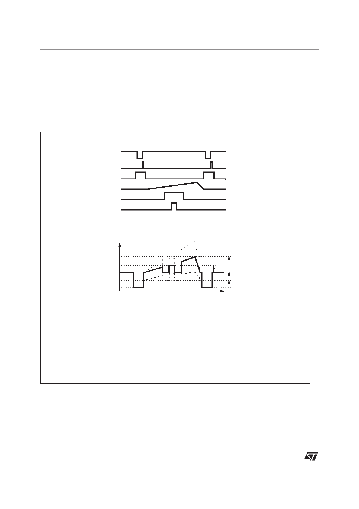
Figure 3. Waveforms VOUT, BRT, CONT, OSD
HSYNC
BPCP
BLK
Video IN
FBLK
OSD IN
and hold circuit (Register 8, bit 7 = 1 and BLK pin
grounded) so that the output DC level is still controlled by I2C.
To ensurethe device correct behavior in the worst
possible conditions, the Brightness Register must
be set to 0.
Notes :
V
1.
V
2.
V
3.
V
4.
V
5.
DC
BLACK
BRT
CONT
OSD
V
V
V
V
V
0.5 to 2.5V
=
V
=
V
=
V
=
V
=
V
V
OUT1 ,
(4)
CONT
(5)
OSD
(3)
BRT
(2)
BLACK
(1)
DC
+ 0.4V
DC
+ BRT (with BRT = 0 to 2V)
BLACK
+ CONT = k x Video IN (CONT = 4.4VPPmax. for VIN= 0.7VPP)
BRT
+ OSD (OSD max. = 4.9VPP, OSD min = 0VPP)
BRT
OUT2
,V
OUT3
OSD
CONT
BRT
0.4V fixed
6/22
Figure 4. Waveforms (Drive adjustment)
HSYNC
BPCP
BLK
Video IN
BFLK
OSD IN
V
OUT1,VOUT2,VOUT3
V
OSD
V
CONT
TDA9207
V
BRT
V
BLACK
V
DC
Note :
1.Drive adjustment modifies the following voltages : V
Drive adjustment doesn’t modify the following voltages : V
Two examples of drive
adjustment
4.10 Bandwidth Adjustment
A new feature: Bandwidth adjustment, has been
implemented on the TDA9207.
This function has several advantages:
– Depending on the external capacitive load and
on the peak-to-peak output voltage, the bandwidth can be adjusted to avoid any slew-rate
phenomenon.
– The preamp bandwidth can be adjustedinorder
to reduce electromagnetic radiation, sinceit is
possible to slow down the signal rise/fall time at
the CRT driverinput without too much affecting
the rise/fall time at the CRT driver output.
– It is possible to optimize the ratio of the frequen-
cy response versus the CRT driver power consumption for any kind of chassis, as the preamp
bandwidth adjustment also allows the adjustment of the rise/fall timeonthe cathode (through
the CRT driver).
(1)
CONT,VBRT
DC
and V
and V
OSD
BLACK
.
.
– In still picture mode, when a high Video swing
voltage is of greater interest than rise/fall time,
bandwidth adjustmentis used to avoid any slewrate phenomenon attheCRTdriver output and to
meet electromagnetic radiation requirements.
4.11 CRT Cathode Coupling
The powerfull multiplex capability of the TDA9207
allows touse the device with several kinds of CRT
cathode coupling.
4.11.1 AC coupling withDC restore ( Figure 5)
In this mode the output DClevel (VDC) is adjusted
simultaneously for the 3 channels from 0.5 V to
2.35 V via Register 6(4 bits). Thecut-offvoltage is
programmed independently for each channelfrom
0.17 V to 4.6 V using registers 10, 11, 12 (8 bits
each, see I2C Table 1).
7/22

TDA9207
4.11.2 DC Coupling with cut-off controls on
Video Amplifier (with TDA9533/ 9530, Figure 6)
The functioningand programming of the TDA9207
are the same as for the previous mode, except for
4.11.3 DC Coupling Mode (Figure 7)
This is the most commonly used configuration en-
abling to build a powerful video system on a small
PCB Board and giving a substantial cost saving
compared with any other solutionavailable on the
market.
The preamplifieroutputs control directlythe cut-off
levels.
The output DC level (VDC) is adjusted independently for each channel from 0.5V to 2.5 V via registers 10, 11 and 12.
In DC coupling mode, bit 2 must be set to 1 and
bit3 to 0 in Register 9.
Figure 5. AC Coupling
TDA9207
the cut-off control which is now performed via the
Video amplifier cut-off input .
In AC coupling and DC coupling with cut-off control, bits 2, 3 and 4 in Register 9 must be set to 1.
4.11.4 DC Couplingwith feedback mode (Fig. 8)
In thismode, the feedback voltageissued from the
cathode is sent to the TDA9207. This voltage is
compared to a reference from the cut-off DC level
DAC bythe sample and hold circuit whoalso controls the DC voltage of the feedback input in a
range of 0.5 V to 2.5 V.
Each channelis independently controlled via Registers 10, 11 and 12.
In DC couplingwith feedback mode, bit 2 and bit 4
must be set to 0 in Register 9.
17-19-21
Pins
CRT
Driver
CRT
DC LEVEL (4bits)
0.5V to 2.35V
CUT-OFF 1,2,3 DC LEVEL
0.17V to 4.6V(8bits)
Figure 6. DC Coupling with Cut-off Control
TDA9207
DC LEVEL (4bits)
0.5V to 2.35V
CUT-OFF 1,2,3 DC LEVEL
0.17V to 4.6V (8bits)
Pins15-16-22
Pins 17-19-21
Pins 15-16-22
Cut-off Control
CRT
TDA9533/9530
8/22

Figure 7. DC Coupling
TDA9207
TDA 9207
Pins17-19-21
OUTPUT 1,2,3 DC LEVEL
0.5V to 2.5V (8bits)
Figure 8. DC Coupling with Feedback (LCD mode)
TDA 9207
Pins 17-19-21
Pins 15-16-22
CUT-OFF 1,2,3 DC LEVEL
0.5V to 2.5V (8bits)
Driver
CRT
Driver
CRT
CRTCRT
4.12 Stand-by Mode
The TDA9207 has a stand-by mode. As soon as
the VCCpower (Pin 20) gets lower than 3V (typ.),
the device is set in stand-by mode whatever the
voltage on analog V
blocks are internally switched-off while the logic
(Pin 7) is. The analog
CCA
parts (I2C bus, power-on reset) are still supplied.
In stand-by mode, the power consumption is be-
low 20 mW.
4.13 Serial Interface
The 2-wire serial interface is an I2C interface. The
slave address of TDA9207 is DC hex.
A6 A5 A4 A3 A2 A1 A0 W
11011100
The host MCU can write into the TDA9207 registers. Read mode is not available.
In orderto write data into the TDA9207, after the
“start” message, the MCU must sendthefollowing
data (see Figure 9):
– theI2C address slave byte with alow level forthe
R/W bit,
– the byte to the internal register address where
the MCU wants to writedata,
– the data.
All bytes are sent withMSB bit first. Thetransfer of
written data is ended with a “stop” message.
When transmitting several data, the register ad-
dresses and data can be written with no need to
repeat thestart and slave addresses.
9/22

TDA9207
4.14 Power-on Reset
A power-on reset function is implemented on the
TDA9207 so that the I2C registers have a determined status after power-on. The Power-on reset
Figure 9. I2C Write Operation
SCL
SDA
W
2
C SlaveAddressStart
A7 A6 A5 A4 A3 A2 A1 A0
Register Address ACKACKI
threshold for a rising supply on V
CCA
(Pin 7) is
3.8 V (typ.) and 3.2V when the VCCdecreases.
D7 D6 D5 D4 D3 D2 D1 D0
Data Byte ACK Stop
10/22

TDA9207
5 -ABSOLUTE MAXIMUM RATINGS
Symbol Parameter Pin Value Units
V
Max.
CCA
Max.
V
CCP
V
Max. Voltage at any Input Pins (except Video inputs) and Input/Output Pins - 5.5 V
in
Max. Voltage at Video Inputs 1, 3, 5 1.4 V
V
I
T
stg
T
oper
Supply Voltage on Analog V
Supply Voltage on Power V
CC
CC
7
20
Storage Temperature - - °C
Operating Junction Temperature - +150 °C
5.5
8.8
6 -THERMAL DATA
Symbol Parameter Value Units
R
th(j-a)
T
j
Max. Junction-ambient Thermal Resistance 69 °C/W
Typ. Junction Temperature at T
=25°C80°C
amb
7 -DC ELECTRICAL CHARACTERISTICS
T
=25°C, V
amb
Symbol Parameter Test Conditions Min. Typ. Max. Units
V
CCA
V
CCP
I
CCA
I
CCP
V
I
Vo Output Voltage Range 0.5
V
I
L
V
I
H
I
I
N
R
HS
CCA
=5V,V
= 8V, unless otherwise specified.
CCP
Analog Supply Voltage Pin 7 4.5 5 5.5 V
Power Supply Voltage Pin 20 4.5 8 8.8 V
Analog Supply Current V
Power Supply Current V
=5V 70 mA
CCA
=8V 55 mA
CCP
Video Input Voltage Amplitude 0.7 1 V
V
CCP
-0.5V
Low Level Input Voltage
High Level Input Voltage
OSD, FBLK, BLK, HSYNC
0.8 V
2.4
Input Current OSD, FBLK, BLK -1 1 µA
Input Resistor HSYNC 40 kΩ
V
V
V
V
11/22

TDA9207
8 -AC ELECTRICAL CHARACTERISTICS
T
=25°C, V
amb
RS= 100Ω, serial betweenoutput pin and C
Symbol Parameter Test Conditions Min. Typ. Max. Units
VIDEO INPUTS (PINS 1, 3, 5)
V
VIDEO OUTPUT SIGNAL (PINS 17, 19, 21) - GENERAL
GAM Maximum Gain Max Contrast and Drive
VOM Maximum Video Output Voltage
VON
CAR Contrast Attenuation Range
DAR Drive Attenuation Range From Max. Drive (DRV = 254 dec)
GM Gain Matching Contrast and Drive at POR
t
R,tF
BW Large Signal Bandwidth V
BW Bandwidth Adjustment Range V
CT Crosstalk between Video Outputs V
VIDEO OUTPUT SIGNAL — BRIGHTNESS
BRTmax Maximum Brightness Level Max. Brightness (BRT = 255 dec)
BRTmin Minimum Brightness Level Min. Brightness (BRT = 0 dec)
VIP Insertion Pulse 0.4 V
BRTM Brightness Matching Brightness and Drive at POR
VIDEO OUTPUT SIGNAL — OSD
OSDmax
OSDmin
VIDEO OUTPUT SIGNAL — DC LEVEL (AC COUPLING MODE)
DCLmax
DCLmin
DCLstep Output DC Level Step 155 mV
VIDEO OUTPUT SIGNAL — DC LEVEL (DC COUPLING MODE)
DCLmax
DCLmin
DCLstep Output DC Level Step 10 mV
Assuming that VOMremains within the range of Vo (between 0.5V and V
are calculated values, assuming an ideal input rise/fall time of 0ns (tR=
t
R,tF
Video Input Voltage Amplitude Max. Contrast and Drive 0.7 1 V
I
(Note)
Nominal Video Output Voltage
Rise Time, Fall Time (Note)
Maximum OSD Output Level
Minimum OSD Output Level
Maximum Output DC Level
Minimum Output DC Level
Maximum Output DC Level
Minimum Output DC Level
CCA
=5V,V
=8V,Vi= 0.7 VPP,C
CCP
= 5pF
LOAD
, unless otherwise specified.
LOAD
(CRT = DRV = 254 dec)
Max Contrast and Drive
(CRT = DRV = 254 dec)
Contrast and Drive at POR
(CRT = DRV = 180 dec)
From max.Contrast (CRT=254 dec)
to min. Contrast (CRT = 1 dec)
to min Drive (DRV = 1 dec)
=2VPP(BW = 15 dec)
V
OUT
=2VPP(BW = 0 dec)
V
OUT
=2V
OUT
OUT
Minimum bandwidth (BW = 0 dec)
=2V
PP
PP
Maximum bandwidth (BW =15 dec)
OUT
=2V
PP
@ f = 10 MHz
@ f = 50 MHz
and Max. Drive (DRV = 254 dec)
and Max. Drive (DRV = 254 dec)
Max. Drive (DRV = 254 dec)
Max. OSD (OSD = 15 dec)
Min. OSD (OSD = 0 dec)
Max. DCL (DCL= 15 dec)
Min. DCL (DCL = 3 dec)
Max. Cut-off (Cut-off = 255 dec)
Min. Cut-off (Cut-off =40 dec)
- 0.5V)
CCP
t
ROUT
2
+t
RIN
16 dB
4.4 V
2.2 V
48 dB
48 dB
±0.1 dB
2.7
4.3
130 MHz
80
130
60
35
2V
0V
±10 mV
4.9
0
2.35
0.5
2.5
0.4
2
,tF
2
=
t
FOUT
+t
FIN
2
ns
ns
MHz
MHz
dB
dB
V
V
V
V
V
V
12/22

TDA9207
AC ELECTRICAL CHARACTERISTICS (continued)
T
=25°C, V
amb
Symbol Parameter Test Conditions Min. Typ. Max. Units
CUT-OFF OUTPUTS (AC COUPLING MODE) - (Pins 15, 16, 22)
COmax Maximum Cut-off Output Level
COmin Minimum Cut-off Output Level
COTD Cut-off Output Voltage Drift T
COHIin
COLIin
COstep Cut-off Output Step (linear region) 20 mV
FEEDBACK INPUTS (DC WITH FEEDBACK MODE)
VFBmax
VFBmin
VFBstep Controlled Feedback Input Level Step 10 mV
IFB input Current on Feedback inputs V 2.5V 50 µA
ABL (PIN 2)
GABLmin
GABLmax
V
ABL
IABLhigh
IABLlow
= 5V, V
CCA
Maximum Cut-off Output Voltage
(linear region)
Minimum Cut-off Output Voltage
(linear region)
= 8V, Vi= 0.7 VPP,C
CCP
= 5 pF, unless otherwise specified
LOAD
Max. Cut-off (Cut-off = 255 dec)
and Sourced Current = 200µA
Min. Cut-off (Cut-off = 0 dec)
and Sinked Current = 2mA
Variation = 100°C 0.5 %
j
Cut-off =235dec
(Sourced Current = 200µA)
Cut-off = 10 dec
(Sinked current = 2mA)
4.7 V
0.1 V
4.6 V
0.17 V
Controlled Feedback Input Level
Maximum
Minimum
Max. Cut-off (Cut-off = 255 dec)
Min. Cut-off (Cut-off = 1 dec)
2.5
20
≤
ABL Mini Attenuation
ABL Maxi Attenuation
V
V
ABL
ABL
3.2 V
≥
=1V
ABL Threshold Voltage For output attenuation 3 V
V
V
ABL
ABL
= 3.2V
=1V
High ABL Input Current
Low ABL Input Current
0
15
0
-2
V
mV
dB
dB
µA
µA
9-I2C ELECTRICAL CHARACTERISTICS
T
=25°C, V
amb
Symbol Parameter Test Conditions Min. Typ. Max. Units
V
IL
V
IH
I
IN
f
SCL(Max.)
V
OL
Low Level Input Voltage On Pins SDA, SCL 1.5 V
High Level Input Voltage 3 V
Input Current (Pins SDA, SCL) 0.4 V < VIN< 4.5 V -10 +10 µA
SCL Maximum Clock Frequency 200 0.25 kHz
Low Level Output Voltage
= 5V,unless otherwise specified
CCA
SDA Pin
when ACK Sink Current = 6mA
0.6 V
13/22

TDA9207
10 -I2C INTERFACETIMING REQUIREMENTS
(see Figure 11)
Symbol Parameter Min. Typ. Max. Units
t
BUF
t
HDS
t
SUP
t
LOW
t
HIGH
t
HDAT
t
SUDAT
t
R,tF
Figure 10. I2C Timing Diagram
Time the bus must be free between two accesses 1300 ns
Hold Time for Start Condition 600 ns
Set-up Time for Stop Condition 600 ns
The Low Period of Clock 1300 ns
The High Period of Clock 600 ns
Hold Time Data 300 ns
Set-up Time Data 250 ns
Rise and Fall Time of both SDA and SCL 20 300 ns
SDA
SCL
t
HDS
t
BUF
t
HIGH
t
SUDAT
t
HDAT
t
SUP
t
LOW
14/22

11 -I2C REGISTER DESCRIPTION
Register Sub-addressed - I2C Table 1
TDA9207
Sub-address
Hex Dec Hex Dec Hex Dec
01 01 Contrast (CRT) 8-bit DAC B4 180 FE 254
02 02 Brightness (BRT) 8-bit DAC B4 180 FF 255
03 03 Drive 1 (DRV) 8-bit DAC B4 180 FE 254
04 04 Drive 2 (DRV) 8-bit DAC B4 180 FE 254
05 05 Drive 3 (DRV) 8-bit DAC B4 180 FE 254
06 06 Output DC Level (DCL) 4-bit DAC 09 09 0F 15
07 07 OSD Contrast (OSD) 4-bit DAC 09 09 0F 15
08 08 BPCP & OCL Refer to the I
09 09 Miscellaneous Refer to the I
0A 10 Cut Off Out 1 DC Level (Cut-off) 8-bit DAC B4 180 FF 255
0B 11 Cut Off Out 2 DC Level (Cut-off) 8-bit DAC B4 180 FF 255
0C 12 Cut Off Out 3 DC Level (Cut-off) 8-bit DAC B4 180 FF 255
0D 13 Bandwidth Adjustment (BW) 4-bit DAC 07 07 0F 15
For Contrast & Drive adjustment, code 00 (dec) and 255 (dec) are not allowed.
For Output DC Level, code 00(dec), 01(dec), 02(dec) are not allowed (Register 06).
For Cut Off Output DC Level, output voltage is linear between code 10 and code 235 (Registers 0A, 0B, 0C).
Register Names
2
C table 2 04 04
2
C table 3 1C 28
POR Value
Max.
Value
BPCP & OCLRegister (R8) - I2C Table 2 (see also Figure12)
b7 b6 b5 b4 b3 b2 b1 b0 Function POR Value
0 0 Internal BPCP triggered by HSYNC x
0 1 Internal BPCP triggered by BLK
0 0 Internal BPCP synchronized by the trailing edge x
0 1 Internal BPCP synchronized by the leading edge
0 0 0 Internal BPCP Width = 0.33 µs
0 0 1 Internal BPCP Width = 0.66 µsx
0 1 0 Internal BPCP Width = 1 µs
0 1 1 Internal BPCP Width = 1.33 µs
1 Internal BPCP = BPCP input (Pin 23)
0 Normal Operation x
1 Reserved (Force BPCP to 1 in test)
0 Normal Operation x
1 Reserved (Force OCL to 1 in test)
0 Internal OCL pulse triggered by BLK (pin 24) x
1 Internal OCL pulse = Internal BPCP
15/22

TDA9207
Miscellaneous Register (R9) - I2C Table 3
b7 b6 b5 b4 b3 b2 b1 b0 Function POR Value
0 Positive Blanking Polarity x
1 Negative Blanking Polarity
0 Soft Blanking = OFF x
1 Soft Blanking = ON
1 1 1 AC Coupling Mode or DC with Cut-off control x
x 0 1 DC Coupling Mode
0 x 0 DC Coupling with Feedback Mode
0 0 Light Grey on OSD Outputs = OFF x
0 1 Light Grey on OSD Outputs = ON
0 0 Dark Grey on OSD Outputs = OFF x
1 0 Dark Grey on OSD Outputs = ON
0 SOG Clipping =OFF x
1 SOG Clipping =ON
Bandwidth Adjustment (R13) - I2C Table 4
b7 b6 b5 b4 b3 b2 b1 b0 Function POR Value
1111130MHz
0111100MHz x
000080MHz
0 0 Normal Operation x
0 1 BW DAC output connected to BLK input (for test)
10
BW DAC complementary output connected to BLK input
(for test)
Figure 11. BPCP andOCL Generation
Source
Selection
R8b0
HS/BPCP
(External)
23
BLK
(External)
24
16/22
Automatic
Polarity
Polarity
Selection
BLK Polarity
Selection
R9b0
HS edge
Selection
R8b1
Edge
Selection
Width
Selection
R8b2b3
Pulse
Generation
Pulse
Generation
BPCP Source
Selection
R8b4
(Internal)
(Internal)
OCL Source
Selection
R8b7
BPCP
OCL

12 -INTERNAL SCHEMATICS
TDA9207
Figure 12.
(Pins1-3-5)
Figure 13.
ABL
IN
Figure 15.
V
CC5
30k
V
CCA
7
(8V)
LOGIC
HIGH
PART
IMPEDANCE
GNDA
GNDA
6
Figure 16.
V
V
CCA
OSD-FBLK-HS-BLK
1k
2
Pins9-10-11
12-23-24
GNDA
CCA
GNDA
GNDL
Figure 14.
GNDL
Figure 17.
V
CCA
HSYNC
4
GNDA
23
GNDA
GNDL
17/22
2

TDA9207
Figure 18.
SCL
13
GNDA
SCA 14
GNDA
Figure 19.
Pins15-16-22
(8V)
CO/FB
30kΩ
4pF
30kΩ
4pF
V
CCA
GNDA
GNDL
GNDL
Figure 21.
GNDP
18
V
CCP
GNDA
Figure 20.
Pins17-19-21
V
CCP
OUT
20
(20V)
GNDA GNDP
18/22

TDA9207
Figure 22. TDA9207/9209 - TDA9533/9530 Demonstration Board: Silk Screen and Trace (scale 1:1)
19/22

TDA9207
Figure 23. TDA9207/9209 - TDA9533/9530 Demonstration Board Schematic
F3(2)
C11
C10(1)
C12(1)
IN2
20
VCCP
IN3
R17
D5
D6(2)
GND2
19
C6(1) 100nF
1N4148
75R
FDH400
L2 .33uH
47uF
100nF
100nF/250V
VDD
OUT2
C_OFF2
GNDS
R18 100R
18
OUT2
GNDP
GNDA
VCCA
5V
3 3
R22 150R / 0.5W
R21 120R/ 0.5W
Rout
IN1
R20 15R/50R
17
OUT3
VDDL/AV
100nF
D7
1N4148
110V
GND1
R24 100R
16
R23 33R
C13
D9(2)
123456789101112131415
OUT1
C_OFF1
15
CUT2
OSD1
101112 13
D8
R25
FDH400
TDA9530/33
C15(1)
C14(1)
SDA
14
SDA
CUT3
OSD2
OSD3
Jump
S3
1N4148
75R
R27 150R / 0.5W
L3 .33uH
R26 120R/ 0.5W
Bout
110V
100nF
100nF
SCL
FBLK SCL
S4
AV
KB
C18
C17
100pF
C16
100pF
TDA9207/09
Jump
OSD1
HEAT
101112
100nF/250V
J4
GND_CRT
Jump
S5
OSD2
F1(2)
C19
10nF/ 400V
9
H2
H1BGND
J3
10
R29
5V
1234567891011
J7
VFly
HFly AV
12
J6
Jump
S6
S7
FBLK
OSD3
2 2
KR
8
R
OSD1
OSD2
VSYNC
5-8V5VHSYNC
Jump
J5
OSD3
F2(2)
G2
7
G2
FBLK
SDA
Bin
C20
SCL
BLANK
HEATG1110V
in
Rin
10nF/ 2KV
G1 G
GND
HSYNC
HFly
HSYNC
VSYNC
G
KG
C25
56
1
VFly
12
OSD
12V
1234567891011
12
11
10
9
8
7
6
5
4
3
2
1
10nF/ 400V
150R
R28
G1
Supply
12V
5-8V
5V
J2 Video
<Doc>
CRT4TDA9207/09+TDA9533
A4
Title
Size DocumentNumber Rev
2: The purpose of all componentsfollowed by (2) is to ensure a
good protectionagainst overvoltage(arcing protection)
1: All capacitors followed by (1) are decoupling capacitors
which must be connectedas close as possibleto the device
Notes:
C23
47uF
C22
47uF
C21
47uF
1 1
11Monday,January 17,2000
Date: Sheet of
E
D
C
B
A
D1(2)
Jump
110V
C24 4.7uF / 150V
R19(2)
33R
110V
SDA
SCL
2K7
2K7
123
4
J1
I2C
C1(1)
R3
2R7
R7 100R
Jump
S2
HSYNC
BLANK
R6
2R7
R5
2R7
R4
2R7
R9 33R
100nF
C4
D2
1N4148
5V
R12
4 4
E
D
R2
R1
5V
C
S1
5V5-8V
B
A
5V
R11 150R/ 0.5W
FDH400
L1 .33uH
12V
R10 120R/ 0.5W
transient response optimisation
Gout
OUT3
GND3
U2
C_OFF3
C3(1)
100nF
R13 100R
R14 15R/50R
100pF
C5(1) 100pF
21
22
23
24
BLK
R8 100R
D3
U1
C2(1) 100nF
1N4148
75R
CUT1
Hs/BPCP
IN1
ABL
IN2
123456789
C9(1) 100nF
R15 33R
100nF
C7
D4
1N4148
5V
110V
VCC
IN3
R16 15R/50R
C8(1) 100nF
OUT1
GNDL
20/22

PACKAGE MECHANICAL DATA
24 Pins — Plastic Dip (Shrink))
A2
A1
LA
TDA9207
E
E1
BeB1
D
24
1
13
12
Stand-off
F
SDIP24
e1
e2
c
E
e3
e2
Millimeters Inches
Dimensions
Min. Typ. Max. Min. Typ. Max.
A 5.08 0.20
A1 0.51 0.020
A2 3.05 3.30 4.57 0.120 0.130 0.180
B 0.36 0.46 0.56 0.0142 0.0181 0.0220
B1 0.76 1.02 1.14 0.030 0.040 0.045
C 0.23 0.25 0.38 0.0090 0.0098 0.0150
D 22.61 22.86 23.11 0.890 0.90 0.910
E 7.62 8.64 0.30 0.340
E1 6.10 6.40 6.86 0.240 0.252 0.270
e 1.778 0.070
e1 7.62 0.30
e2 10.92 0.430
e3 1.52 0.060
.015
0,38
Gage Plane
21/22

TDA9207
Information furnished is believed to be accurate and reliable. However, STMicroelectronics assumes no
responsibility for the consequences of use of such information nor for any infringement of patents or other
rights of third parties which may result from its use. No license is granted by implication or otherwise under any
patent orpatent rights of STMicroelectronics. Specifications mentioned inthispublication are subject to change
without notice. This publication supersedes and replaces all information previously supplied.
STMicroelectronics products are not authorized for use as critical components in life support devices or
systems without express written approval of STMicroelectronics.
The ST logo is a trademark of STMicroelectronics.
2000 STMicroelectronics - All Rights Reserved
Purchase of I
Rights to use these components in a I
Australia - Brazil - China - Finland - France - Germany - Hong Kong - India - Italy - Japan -Malaysia - Malta - Morocco
22/22
2
C Components of STMicroelectronics, conveys a license under the Philips I2C Patent.
Standard Specifications as defined by Philips.
STMicroelectronics GROUP OF COMPANIES
Singapore - Spain - Sweden - Switzerland - United Kingdom - U.S.A.
2
C system, is granted provided that the system conforms to the I2C
http://www.st.com
3
 Loading...