

I2C BUS CONTROLLED 70MHz RGB PREAMPLIFIER
.
70MHz TYPICAL BANDWIDTH AT 4VPPOUTPUTWITH12pFCAPACITIVELOAD
.
5.5ns TYPICAL RISE/FALL TIME AT 4V
OUTPUTWITH 12pF CAPACITIVELOAD
.
POWERFULLOUTPUTDRIVE CAPABILITY
.
BRT, CONT, DRIVE, OUTPUT DC LEVEL,
OSD CONTRAST, BACK-PORCH CLAMPING
PULSEWIDTH AREI
.
INTERNAL BACK-PORCH CLAMPING
PULSEGENERATOR
.
OSD WHITEBALANCETRACKING
.
INTERNALOSD SWITCHES
.
BLANKINGAND FAST-BLANKINGINPUTS
.
VERY LARGE DRIVE ADJUSTMENT RANGE
(48dB)
.
SEMI-TRANSPARENT BACKGROUND ON
OSD PICTURE
.
ABLCONTROL
2
C BUS CONTROLLED
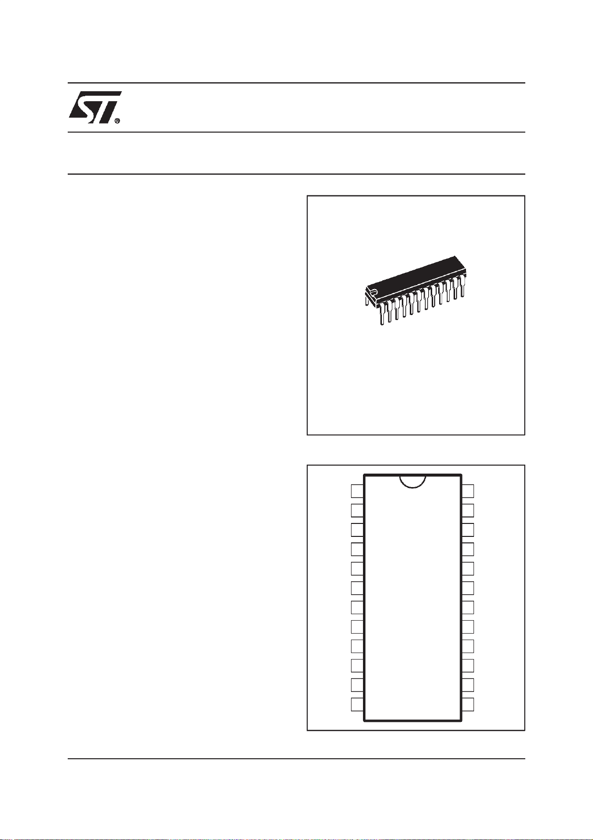
TDA9203A
PP
SHRINK 24
(Plastic Package)
ORDER CODE : TDA9203A
DESCRIPTION
The TDA9203A is a digitaly controlled wideband
video preamplifier intended for use in mid range
color monitor. All controls and adjustments are
digitaly performed thanks to I
trast, brightness and DC output level of RGB signals are common to the 3 channels and drive
adjustmentisseparatefor eachchannel.ThreeI
gain controlled OSD inputs can be switched with
RGBsignalsusingfastblankingcommand.Clampingof RGBsignalsis performedthanksto aflexible
integrated system. The white balance adjustment
is effectiveon brightness,video and OSD signals.
The TDA9203Aworks for application using AC or
DC coupledCRT driver.
The ABL input provides a 12dB Max. attenuation
on the current contrast value according average
beamlimitation voltage.
Because of its features and due to component
saving the TDA9203Aleads to a very performant
and cost effectiveapplication.
2
C serial bus. Con-
2
C
PIN CONNECTIONS
IN1
OSD1
AV
IN2
OSD2
AGND
IN3
OSD3
ABL
LGND
SDA
SCL
DD
1
2
3
4
5
6
7
8
9
10
11
12
24
23
22
21
20
19
18
17
16
15
14
13
HSYNC
PV
CC1
OUT1
PGND1
PV
CC2
OUT2
PGND2
PV
CC3
OUT3
PGND3
BLK
FBLK
9203A-01.EPS
June 1998
1/13
TDA9203A
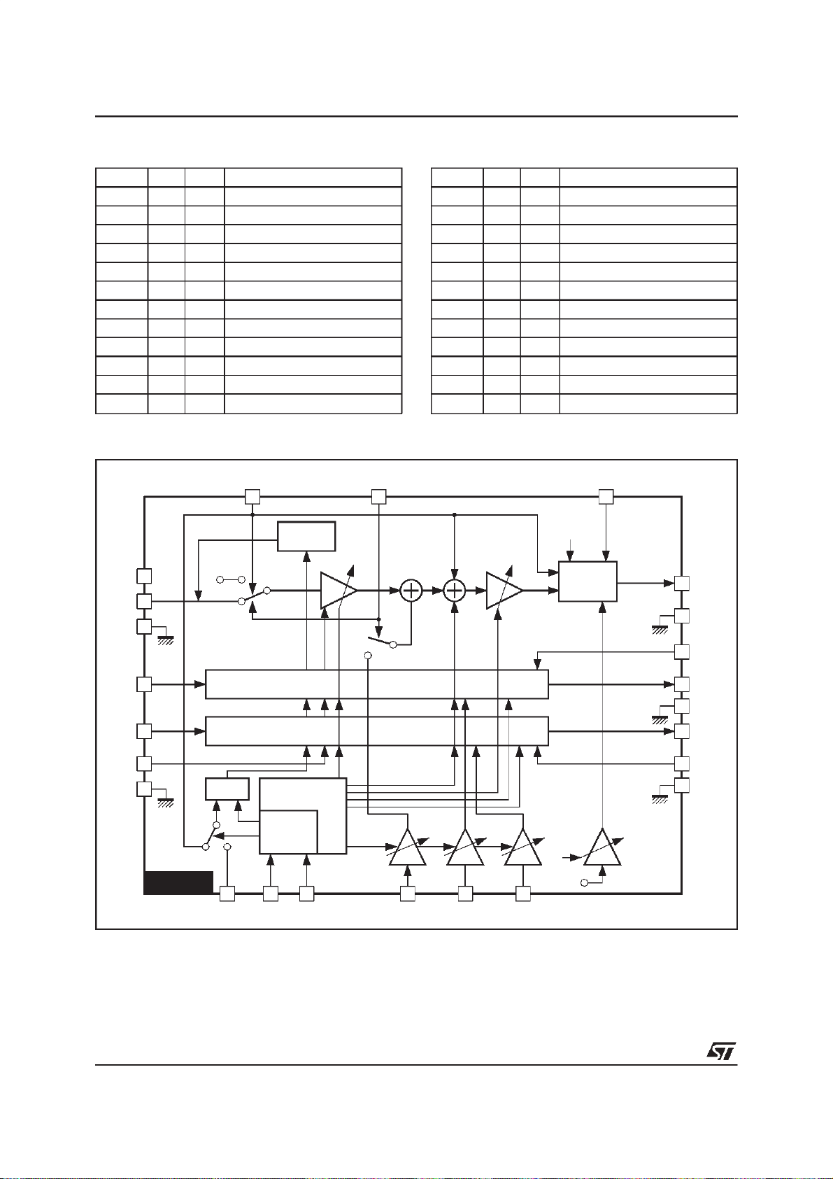
PIN DESCRIPTION
Name Pin Type Function
IN1 1 I 1
OSD1 2 I 1
AV
3 I 12V Analog V
DD
IN2 4 I 2ndChannel Main Picture Input
OSD2 5 I 2
AGND 6 I/O Analog Ground
IN3 7 I 3
OSD3 8 I 3
ABL 9 I ABL Input
LGND 10 I/O Logic Ground
SDA 11 I/O Serial Data Line
SCL 12 I Serial Clock Line
BLOCKDIAGRAM
st
Channel Main Picture Input
st
Channel OSD Input
DD
nd
Channel OSD Input
rd
Channel Main Picture Input
rd
Channel OSD Input
Name Pin Type Function
FBLK 13 I Fast Blanking Input
BLK 14 I Blanking Input
rd
PGND3 15 I/O 3
OUT3 16 O 3
PV
17 I 3rdChannel Power V
CC3
Channel Power Ground
rd
Channel Output
CC
PGND2 18 I/O 2ndChannel Power Ground
nd
OUT2 19 O 2
PV
20 I 2ndChannel Power V
CC2
Channel Output
CC
PGND1 21 I/O 1stChannel Power Ground
st
OUT1 22 O 1
PV
23 I 1stChannel Power V
CC1
Channel Output
CC
HSYNC 24 I Horizontal Synch Input
9203A-01.TBL
AV
IN1
AGND
IN2
IN3
ABL
LGND
3
DD
1
6
4
7
9
10
TDA9203A
V
REF
BLUECHANNEL
GREEN CHANNEL
BPCP
24
LATCHES
BUS
DECODER
11 12
CLAMP
2
C
I
SCLSDAHSYNC
FBLKBLK
CONTRAST
D/A
OSD
CONT
1314
BRIGHTNESS
2
OSD1 OSD2 OSD3
5
DRIVE
8 bits
8
2
C
I
BPCP
OUTPUT
STAGE
V
REF
PV
CC1
23
OUTPUT
DC LEVEL
ADJUST
22
21
20
19
18
16
17
15
OUT1
PGND1
PV
CC2
OUT2
PGND2
OUT3
PV
CC3
PGND3
9203A-02.EPS
2/13
FUNCTIONAL DESCRIPTION
InputStage
The R, G and B signals must be fed to the three
inputsthroughcoupling capacitors(100nF).
Themaximuminput peak-to-peakvideo amplitude
is 1V.
Theinput stage includesa clampingfunction.This
clamp is using the input serial capacitor as ”memory capacitor”and is gatedby an internally generated”Back-Porch-Clamping-Pulse(BPCP)”.
Thesynchronizationedge of the BPCPis selected
accordingbit 0 of registerR8.
WhenB0R8 is set to 1, the BPCPis synchronized
ontheleadingedgeoftheblankingpulseBLKinputs
onPin14(seeFigure1).B7R8allowstousepositive
or negativeblankingsignal on Pin 14. Atpower on
resetTDA9203Ause onlypositive blanking.
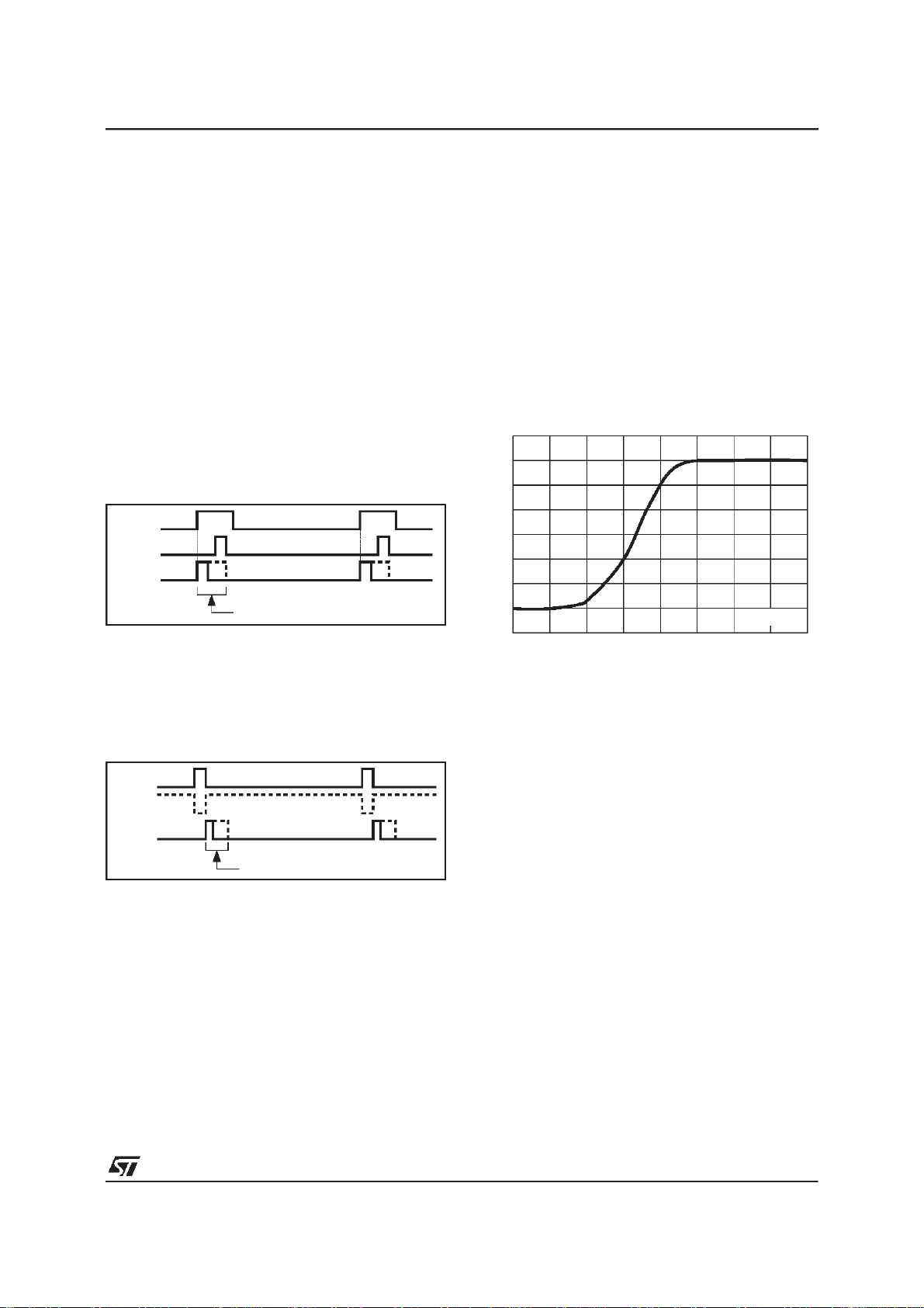
Figure1
BLK
HSYNC
BPCP
2
Internal pulse width is controlled by I
C
WhenB0R8is clearto0, theBPCPissynchronized
onthesecondedgeof thehorizontalpulseHSYNC
inputs on Pin 24. An automatic function allows to
usepositive or negativehorizontalpulseon Pin24
(seeFigure 2).
Figure2
HSYNC
BPCP
2
Internal pulse width is controlled by I
In both case BPCP width is adjustable by I
C
2
C, B1
and B2 of registerR8 (see R8 TableP8).
Contrast Adjustment (8 bits)
The contrast adjustment is made by controlling
simultaneously the gain of three internal variable
gain amplifiers throughthe I
2
C bus interface.
The contrast adjustment allows to cover a typical
range of 48dB.
ABLControl
The TDA9203AI
2
C preamplifier provides an ABL
input (automatic beam limitation) to attenuate
TDA9203A
R,G,Bvideo signals according to beam intensity.
The operating range is 2.5V typicaly,from 5.3V to
2.8V.A typical 12dBMax. attenuationis appliedto
the signal whatever the current gain is. Refer to
Figure 3 forABL input attenuationrange.
In case of software control,the ABLinput must be
pulled to AV
consumption(see Figure 11).
ABL input voltage must not exceeed AV
resistoris 10kΩ and equivalentschematic givenin
Figure 11.
Figure 3
Attenuation (dB)
2
0
-2
-4
-6
-8
-10
-12
9203A-03.EPS
-14
123456789
BrightnessAdjustment (8 bits)
As for the contrast adjustment, the brightness is
controlledby I
The brightnessfunction consiststo add the same
DC offsetto the threeR,G, B signalsafter contrast
amplification. This DC-Offset is present only outside the blankingpulse (see Figure 4).
The DC output level during the blanking pulse, is
forced to”INFRA-BLACK”level (V
DriveAdjustment (3x 8 bits)
9203A-04.EPS
Inordertoadjustthewhitebalance, theTDA9203A
offersthepossibilitytoadjustseparatelythe overall
gain of each complete video channel. The gain of
each channel is controlledby I
Theverylargedriveadjustmentrange(48dB)allows
differentstandardor customcolortemperature.
It can also be usedto adjustthe outputvoltagesat
the optimum amplitude to drive the C.R.T drivers,
keepingthewholecontrastcontrolforend-useronly.
The drive adjustment is located after the CONTRAST,BRIGHTNESSand OSDswitchblocks,so
that the white balance will remains correct when
BRT is adjusted, and will also be correct on OSD
portionof the signal.
through a resistor to limit power
DD
2
C.
).
DC
2
C (8bits each).
DD
. Input
VIN(V)
9203A-0X .EPS
3/13

TDA9203A
FUNCTIONAL DESCRIPTION(continued)
OSD Inputs
TheTDA9203Aincludes allthe circuitrynecessary
tomixOSDsignals intotheRGBmain-picture.Four
pins arededicated to this function as follow.
Three TTL RGB On Screen Displayinputs (Pin 2,
5 and 8). These three inputs are connectedto the
three outputs of the corresponding ON-SCREENDISPLAYprocessor(ex : STV942x).
One Fast Blanking Input (FBLK, Pin 13) which is
also connected to the FBLK output of the same
ON-SCREEN-DISPLAYprocessor.
When a high level is present on FBLK, the IC will
acts as follow:
- The three main picture RGB input signals are
internally switched to the internal input clamp
referencevoltage.
- The three output signals are set to voltages correspondingto the state(0 or 1)on thethree OSD
inputs (see Figure4).
Example:
If FBLK = 1 and OSD1, OSD2, OSD3) = 1, 0, 1
respectively.
Then OUT1, OUT2, OUT3 will be equal to V
V
BRT,VOSD
where: V
BRTis the brightnessDC level I
,
BRT=VBLACK
+ BRT, V
OSD=VBRT
2
C adjustable.
OSD is the On-Screen Display signal value I
adjustablefrom 0V to 5.5V
bystep of 0.36V.
PP
Semi-transparent function is controlled thanks to
Bit6 of R8register(seeTable1).
When semi-transparent mode is activated, video
signalis dividedby 2 (CONT).
Table 1
FBLK OSD1 OSD2 OSD3 B6R8
0 x x x 0 Video
1 x x x 0 OSD (1)
0 x x x 1 Video
1 0 x x 1 OSD
1x1x1 OSD
1xx01 OSD
1 1 0 1 1 Semi-trans-
Notes : 1. All OSD colors are displayed.
2. One OSD color is displayed as semi-transparent video
without effect on brightness and DC level adjustment.
Signal (OUTn)
parent (2)
+ OSD
Output
OSD
2
C
Output Stage
Thethreeoutputstagesincorporatethreefunctions
which are :
- The blanking stage : When high level is applied
to the BLK input (Pin 14), the three outputs are
switchedto a voltagewhich is 400mV lower than
the BLACK level. The black level is the output
voltagewithminimumbrightness wheninput signal video amplitude is equalto ”0”.
- The output stage itself : It is a large bandwidth
output amplifier whichallow to deliverup to 5V
on the threeoutputs(for 0.7V videosignal onthe
inputs).
- The output CLAMP : The IC also incorporates
three internal output clamp (sample and hold
system) which allow to DC shift the three output
signals. The DC output voltage is adjustable
through I
2
C with4 bits. Practicaly, the DC output
level allowto adjustthe BLK level (V
underV
)from0.9Vto 2.9Vwith12 x165mV.
BLACK
Theoverallwaveforms ofthe outputsignalaccording to the different adjustment are shown in Fig-
,
ures 4 and 5.
Serial Interface
2
The 2-wiresserial interface is an I
C interface.
The slave address of the TDA9203A is DC (in
hexadecimal).
A6 A5 A4 A3 A2 A1 A0 W
11011100
Data Transfer
The host MCU can write data into the TDA9203A
registers.Read mode is not available.
To write data into the TDA9203A,after a start,the
MCU must send (see Figure6) :
2
- The I
C addressslavebytewitha lowlevel forthe
R/W bit.
- The byte of the internal register address where
the MCU wants to write data(s).
- The data.
All bytes are sent MSB bit first and the write data
transteris closedby a stop.
=400mV
DC
PP
4/13

FUNCTIONAL DESCRIPTION(continued)
Figure4 : WaveformsVOUT, BRT, CONT, OSD
HSYNC
BPCP
BLK
Video IN
FBLK
OSD IN
V
OUT1,VOUT2,VOUT3
(4)
V
CONT
(5)
V
OSD
(3)
V
BRT
(2)
V
BLACK
(1)
V
DC
OSD
TDA9203A
CONT
BRT
0.4V fixed
Notes : 1. VDC= 0.5 to 2.5V
2. V
BLACK=VDC
3. V
BRT=VBLACK
4. V
CONT=VBRT
5. V
OSD=VBRT
+ 0.4V
+ BRT (with BRT = 0 to 2.5V)
+ CONT with CONT= k x Video IN (CONT = 5VPPmax. for VIN= 0.7VPP)
+ OSD with OSD = k1 x OSDIN (OSD max. = 5.5VPP, OSD min. = 360mVPP)
Figure5 : Waveforms(DRIVEadjustment)
HSYNC
BPCP
BLK
Video IN
FBLK
OSD IN
V
OUT1,VOUT2,VOUT3
V
OSD
V
BRT
V
BLACK
V
DC
Two exemples
of drive adjustment
9203A-06.EPS
V
CONT
(1)
Note : 1. Drive adjustment modifies the following voltages: V
Figure6 : I2C Write Operation
SCL
SDA
2
C Slave AddressStart
Drive adjustment do not modify thefollowing voltages : V
W
A7 A6 A5 A4 A3 A2 A1 A0
Register Address ACKACKI
and V
and V
.
OSD
.
BLACK
Data Byte ACK Stop
CONT,VBRT
DC
D7 D6 D5 D4 D3 D2 D1 D0
9203A-07.EPS
9203A-08.EPS
5/13

TDA9203A
QUICK REFERENCEDATA
Symbol Parameter Min. Typ. Max. Unit
Signal Bandwidth (4V
Rise and Fall Time (4V
Drive Adjustment Range on the 3 Channels separately 48 dB
Maximum Output Voltage (V
Output Voltage Range (AC + DC) 8 V
ABSOLUTEMAXIMUM RATINGS
Symbol Parameter Value Unit
V
V
V
V
V
ESD
T
T
T
oper
Supply Voltage (Pins 3-9-17-20-23) 14 V
S
Voltage at any Input Pins (except SDA & SCL & Logical Inputs) GND < V
IN1
Voltage at Input Pins SDA & SCL GND < V
IN2
Voltage at Logical Inputs (OSD, FBLK, BLK, HSYNC) GND < V
IN3
ESD Susceptability (Human body model ;100pF Discharge through 1.5kΩ)2kV
Storage Temperature - 40, + 150 °C
stg
Junction Temperature 150 °C
j
Operating Temperature 0, + 70 °C
/12pF load) 70 MHz
PP
/12pF load) 5.5 ns
PP
= 0.7 VPP)5V
IN
IN1<VS
< 5.5 V
IN2
< 5.5 V
IN3
PP
9203A-02.TBL
V
9203A-03.TBL
THERMAL DATA
Symbol Parameter Value Unit
R
th (j-a)
DC ELECTRICALCHARACTERISTICS (T
Symbol Parameter Test Conditions Min. Typ. Max. Unit
V
I
V
V
V
V
I
Junction-ambient Thermal Resistance 69
=25oC, VCC= 12V,unless otherwise specified)
amb
Supply Voltage Pins 3-9-17-20-23 10.8 12 13.2 V
S
Supply Current (All VSPin current) RL=1kΩ 60 mA
S
Video Input Voltage Amplitude Pins 1-4-7 0.7 1 V
I
Typical Output Voltage Range Pins 16-19-22 0.5 - 8 V
O
Low Level Input (OSD, FBLK, BLK, HSYNC) Pins 2-5-8-13-14-24 0.8 V
IL
High Level Input (OSD, FBLK, BLK, HSYNC) Pins 2-5-8-13-14-24 2.4 V
IH
Input Current (OSD, FBLK, BLK, HSYNC) 0.4V < VIN< 4.5V -10 +10
IN
o
C/W
µ
PP
9203A-04.TBL
A
9203A-05.TBL
6/13

TDA9203A
AC ELECTRICALCHARACTERISTICS
=25oC, VCC= 12V,CL= 12pF,RL=1kΩ , unless otherwisespecified)
(T
amb
Symbol Parameter Test Conditions Min. Typ. Max. Unit
AV Maximum Gain (20 log x V
OUT AC/VIN AC
CAR Contrast Attenuation Range V
DAR Drive Attenuation Range 48 dB
GM Gain Match V
BW Bandwidth Large Signal At -3dB, V
DIS Video Output Distorsion (see Note) f = 1MHz, V
t
R,tF
Video Output Rise and Fall Time
(see Note)
BRT Brightness Maximum DC Level
Brightness Minimum DC Level
BRTM Brightness Matching BRT = 50%, Drive at POR ±20 mV
OSD
CAR
Contrast Attenuation Range
for OSD Input
DC Output Maximum DC Level
Output Minimum DCLevel
Equivalent Load on Video Output with Tj≤ T
R
L
CT Croostalk between Video Channels
(see Note)
G
I
R
Note : These parameters are not tested on each unit. They are measured during an internal qualification procedure which includes
ABL Min. Attenuation
ABL
ABL Max. Attenuation
ABL Input Current V
ABL
ABL Input Resistor See Figure 11 10 kΩ
ABL
characterization on batches coming from corners of our processes and also from temperature characterization.
) Contrast & Drive at maximum 18 dB
= 0.7VPP, Contrast& Drive at POR 48 dB
IN
= 2.5VPP,VIN= 0.7V
OUT
Contrast = Drive = Maxi x 0.7
PP
± 0.1 dB
(power-on reset value)
= 0.7VPP,V
Contrast = Drive = Maxi x 0.87
VIN = 0.7VPP,V
Contrast = Drive = Maxi x 0.87
IN
=1VPP,VIN=1V
OUT
OUT
=4V
OUT
PP
=4V
PP
PP
70 MHz
0.3 %
5.5 ns
2.5
0
V
V
24 dB
j Max.
= 2.5VPP,VIN= 0.7V
V
OUT
Contrast = Drive = Maxi x 0.7
PP
2.5
0.5
1kΩ
44 dB
V
V
(power-on reset value)
= 1MHz
f
IN
V
= 5.3V Typical
ABL
= 2.8V Typical
V
ABL
= 5.3V 20
ABL
0
12
dB
dB
µ
A
9203A-06.TBL
I2C ELECTRICAL CHARACTERISTICS (T
=25oC, VCC= 12V,unless otherwise specified)
amb
Symbol Parameter Test Conditions Min. Typ. Max. Unit
V
IL
V
IH
I
IN
f
SCL(Max.)
V
OL
Low Level Input Voltage On Pins SDA, SCL 1.5 V
High Level Input Voltage 3 V
Input Current (Pins SDA, SCL) 0.4V < VIN< 4.5V -10 +10 µA
SCL Maximum Clock Frequency 200 kHz
Low Level Output Voltage SDA Pin when ACK
0.6 V
Sink Current = 6mA
9203A-08.TBL
7/13

TDA9203A
2
I
C INTERFACE TIMINGS REQUIREMENTS(see Figure 7)
Symbol Parameter Min. Typ. Max. Unit
t
BUF
t
HDS
t
SUP
t
LOW
t
HIGH
t
HDAT
t
SUDAT
t
R,tF
Figure7
Time the bus must be free between 2 access 1300 ns
Hold Time for Start Condition 600 ns
Set-up Time for Stop Condition 600 ns
The Low Period of Clock 1300 ns
The High Period of Clock 600 ns
Hold Time Data 300 ns
Set-up Time Data 250 ns
Rise and Fall Time of both SDA and SCL 20 300 ns
9203A-09.TBL
SDA
SCL
t
HDS
t
BUF
t
HIGH
t
SUDAT
t
HDAT
t
SUP
t
LOW
9203A-09.EPS
8/13

TDA9203A
REGISTERDESCRIPTION
RegistersSub-address
Address (Hex) Register Names Function POR Value
01 Contrast DAC 8-bit B4
02 Brightness DAC8-bit B4
03 Drive 1 DAC 8-bit B4
04 Drive 2 DAC 8-bit B4
05 Drive 3 DAC 8-bit B4
06 Output DC Level DAC 4-bit 08
07 OSD Contrast DAC 4-bit 08
08 BP and Miscellaneous See R8 Table 04
Contrast Register (R1)(Video IN = 0.5VPP, Brightnessat minimum,Drive at maximum)
Hex b7 b6 b5 b4 b3 b2 b1 b0 CONT (VPP) G (dB) POR Value
00 00000000 0 01 00000001 0.015 -30
02 00000010 0.031 -24
04 00000100 0.062 -18
08 00001000 0.125 -12
10 00010000 0.25 -6
20 00100000 0.5 0
40 01000000 1 6
80 10000000 2 12
B4 10110100 2.812 15 X
FF 11111111 4 18
Brightness Register (R2) (Driveat maximum)
Hex b7 b6 b5 b4 b3 b2 b1 b0 BRT (V) POR Value
00 00000000 0
01 00000001 0.010
02 00000010 0.020
04 00000100 0.040
08 00001000 0.080
10 00010000 0.160
20 00100000 0.320
40 01000000 0.640
80 10000000 1.28
B4 10110100 1.8 X
FF 11111111 2.56
9/13

TDA9203A
REGISTERDESCRIPTION (continued)
Drive Registers (R3, R4, R5) (VideoIN = 0.5V
Hex b7 b6 b5 b4 b3 b2 b1 b0 CONT (VPP) G (dB) POR Value
00 00000000 0 -
01 00000001 0.015 -30
02 00000010 0.031 -24
04 00000100 0.062 -18
08 00001000 0.125 -12
10 00010000 0.25 -6
20 00100000 0.5 0
40 01000000 1 6
80 10000000 2 12
B4 10110100 2.812 15 X
FF 11111111 4 18
OutputDC Level Register (R6)
Hex b7 b6 b5 b4 b3 b2 b1 b0 DC (V) POR Value
03 00000011 0.52
04 00000100 0.69
08 00001000 1.35 X
0F 00001111 2.5
Code 00Hex, 01Hex and 02Hex :not to be used
, Brightnessat minimum,Contrast at maximum)
PP
OSD Contrast Register (R7) (V
Hex b7 b6 b5 b4 b3 b2 b1 b0 OSD (V) G (dB) POR Value
00 00000000 0 -
01 00000001 0.36 -24
02 00000010 0.73 -18
04 00000100 1.46 -12
08 00001000 2.93 -6 X
0F 00001111 5.5 0
OSD IN
= 2.4V
.., Driveat maximum)
Min
BP andMiscellaneousRegister(R8)
b7 b6 b5 b4 b3 b2 b1 b0 Function POR Value
0 BP Source = HSYNC X
1 BP Source = BLK
0 0 BP Pulse Width = 0.33µs
0 1 BP Pulse Width = 0.66µs
1 0 BP Pulse Width = 1µsX
1 1 BP Pulse Width = 1.3µs
0 0 Test Purposes X
0 0 0 Soft Blanking OFF X
1 1 1 Soft Blanking ON
0 Semi Transparent OFF X
1 Semi Transparent ON
0 Positive BlankingPolarity Selection X
1 Negative Blanking Polarity Selection
10/13

INTERNAL SCHEMATICS
Figure8
AV
DD
IN
Pins
1-4-7
AGND
Figure10
AGND
Figure9
9203A-10.EPS
Figure11
OSD - BLK- FBLK
Pins 2-5-8-13-14
TDA9203A
AV
DD
AGND AGND
9203A-11.EPS
Figure12
Figure14
AV
AGND
DD
3
(20V)
6
10LGND
AV
DD
AGND
LGND
9203A-12.EPS
Figure13
11-12
9203A-14.EPS
Figure 15
SDA
SCL
Pins
9ABL
AGND
AV
DD
AGND
(10V)
10kΩ
Internal
5V
LGND
9203A-13.EPS
9203A-15.EPS
HSYNC
24
AV
DD
AGND
LGND
Pins 17-20-23
Pins 15-18-21
9203A-16.EPS
PV
CC
PGND
AV
DD
AGND
OUT
Pins 16-19-22
9203A-17.EPS
11/13

TDA9203A
APPLICATION DIAGRAM
SYNCHRO
EXTRACTOR
+5V
33pF
8MHz
GND B
GND R
GND G
GND
100nF
B
R
G
33pF
1
FBLK
VSYNC
2
3
HSYNC
4
V
PXCK
5
CKOUT
6
XTAL OUT
7
XTAL IN
8
+12V
100nF
47
Ω
1kΩ
75Ω
100nF
47Ω
1kΩ
75Ω
100nF
47Ω
75Ω
DD
1k
Ω
TEST
16
B
GND
RESET
SDA
SCL
15
G
14
R
13
12
11
10
9
S
T
V
9
4
2
6
+5V
10µF
16V
100nF
1k
100nF
2.7kΩ
1
IN1
OSD1
2
AV
3
DD
4
IN2
5
OSD2
6
AGND
7
Ω
IN3
8
OSD3
ABLABL
9
LGND
10
SDA
11
SCL
12 13
GND GND
100
Ω
1k
22pF
HSYNC
PV
CC1
OUT1
T
PGND1
D
PV
Ω
OUT2
PGND2
PV
OUT3
PGND3
BLK
FBLK
SDA
SCL
CC2
CC3
I
A
9
2
0
3
A
24
23
22
21
20
19
18
17
16
15
14
2
C BUS
100nF
100nF
100nF
BLK
HSYNC
VSYNC
BLUE OUT
RED OUT
GREENOUT
9203A-18.EP S
12/13

PACKAGE MECHANICAL DATA
24 PINS - PLASTICDIP (SHRINK)
BeB1
TDA9203A
E
E1
A2
A1
LA
Stand-off
c
D
e1
e2
E
13
F
12
SDIP24
e3
e2
.015
0,38
Gage Plane
Dimensions
24
1
Millimeters Inches
Min. Typ. Max. Min. Typ. Max.
A 5.08 0.20
A1 0.51 0.020
3.05 3.30 4.57 0.120 0.130 0.180
B 0.36 0.46 0.56 0.0142 0.0181 0.0220
B1 0.76 1.02 1.14 0.030 0.040 0.045
C 0.23 0.25 0.38 0.0090 0.0098 0.0150
D 22.61 22.86 23.11 0.890 0.90 0.910
E 7.62 8.64 0.30 0.340
E1 6.10 6.40 6.86 0.240 0.252 0270
e 1.778 0.070
e1 7.62 0.30
e2 10.92 0.430
e3 1.52 0.060
L 2.54 3.30 3.81 0.10 0.130 0.150
Information furnished is believed to be accurate and reliable. However, STMicroelectronics assumes no responsibility for the
consequences of use of such information nor for any infringement of patents or other rights of third parties which may result from
its use. No licence is granted by implication or otherwise under any patent or patent rights of STMicroelectronics. Specifications
mentioned in this publication are subject to change without notice. This publication supersedes and replaces all information
previouslysupplied.STMicroelectronics productsarenotauthorizedfor use ascritical componentsin lifesupport devicesor systems
without express written approval of STMicroelectronics.
The ST logo is a trademark of STMicroelectronics
PMSDIP24.EPS
SDIP24.TBL
1998 STMicroelectronics - All Rights Reserved
2
Purchase of I
Rights to use these components in a I
C Components of STMicroelectronics, conveys a licenseunder the PhilipsI2C Patent.
2
C Standard Specifications as defined by Philips.
the I
2
C system,is granted provided that the system conforms to
STMicroelectronics GROUP OF COMPANIES
Australia - Brazil - Canada- China - France - Germany - Italy - Japan - Korea - Malaysia - Malta- Mexico - Morocco - The Netherlands
Singapore - Spain - Sweden - Switzerland - Taiwan - Thailand - United Kingdom- U.S.A.
13/13
 Loading...