

TDA9115
LOW-COST I2C CONTROLLED DEFLECTION PROCESSOR
FOR MULTISYNC MONITOR
FEATURES
General
2
■ I
C-BUS-CONTROLLED
DEFLECTION PROCESSOR DEDICATED
FOR LOW-END CRT MONITORS
■ SINGLE SUPPLY VOLTAGE 12V
■ VERY LOW JITTER
■ DC/DC CONVERTER CONTROLLER
■ ADVANCED EW DRIVE
■ AUTOMATIC MULTISTANDARD
SYNCHRONIZATION
■ DYNAMIC CORRECTION WAVEFORM
OUTPUT
■ X-RAY PROTECTION AND SOFT-START &
STOP ON HORIZONTAL AND DC/DC DRIVE
OUTPUTS
Horizontal section
■ 150 kHz maximum frequency
■ Corrections of geometric asymmetry:
Pin cushion asymmetry, Parallelogram
■ Tracking of asymmetrycorrections with vertical
size and position
■ Horizontal moiré cancellation output
Vertical section
■ 200 Hz maximum frequency
■ Vertical ramp for DC-coupled output stage with
adjustments of: C-correction, S-correction for
super-flat CRT, Vertical size, Vertical position
■ Vertical moiré cancellation through vertical
ramp waveform
■ Compensation of vertical breathing with EHT
variation
EW section
■ Symmetricalgeometrycorrections:Pin cushion,
Keystone
■ Horizontal size adjustment
■ Tracking of EW waveform with Vertical sizeand
position and adaptation to frequency
■ Compensation of horizontal breathing through
EW waveform
Dynamic correction section
■ Vertical dynamic correction waveformoutput for
dynamic corrections like focus, brightness
uniformity, ...
■ Fixed on screen by means of tracking system
DC/DC controller section
■ Step-up and step-down conversion modes
■ External sawtooth configuration
■ Synchronization on hor. frequency with phase
selection
■ Selectable polarity of drive signal
DESCRIPTION
The TDA9115 is a monolithic integrated circuit assembled in a 32-pin shrink dual-in-line plastic
package. This IC controls all the functions related
to horizontal and vertical deflection in multimode
or multi-frequency computer display monitors.
The deviceonly requiresvery fewexternal components.
Combined with other ST components dedicated
for CRTmonitors (microcontroller, video preamplifier, video amplifier, OSD controller) the TDA9115
allows fully I2C bus-controlled computer display
monitors to be built with a reduced number of external components.
SHRINK 32 (Plastic Package)
ORDER CODE: TDA9115
Version 4.0
August 2001 1/45
1

TABLE OF CONTENTS
1 -PIN CONFIGURATION . . . . . . . . . . . . . . . . . . . . . . . . . . . . . . . . . . . . . . . . . . . . . . . . . . . . . . . . 3
2 -BLOCK DIAGRAM . . . . . . . . . . . . . . . . . . . . . . . . . . . . . . . . . . . . . . . . . . . . . . . . . . . . . . . . . . . 4
3 -PIN FUNCTION REFERENCE . . . . . . . . . . . . . . . . .. .. . . . . . . . . . . . . . . . . . . . . . . . . . . . . . . . 5
4 -QUICK REFERENCE DATA . . . . . . . . . . . . . . . . . . . . . . . . . . . . . . . . . . . . . . . . . . . . . . . . . . . . 6
5 -ABSOLUTE MAXIMUM RATINGS . . . . . . . ........................................ 7
6 -ELECTRICAL PARAMETERS AND OPERATING CONDITIONS . . . . . . ................. 8
6.1 THERMAL DATA . . . . . . .. . . . . . . . . . . . . . . . . .. .. . . . . . . . . . . . . . . . . . . . . . . . . . . . . . 8
6.2 SUPPLY AND REFERENCE VOLTAGES . . . . . . . . . . . . . . . . . . . . . . . . . . . . . . . . . . . . . . 8
6.3 SYNCHRONIZATION INPUTS . . . . . . . . . . . . . . . . . . . . . . . . . . . . . . . . . . . . . . . . . . . . . . 8
6.4 HORIZONTAL SECTION . . . . . . . . . . . . . . . . . . . . . . . . . .. . . . . . . . . . . . . . . . . . . . . . .. . 9
6.5 VERTICAL SECTION . . . . . . . . . . . . . . . . . . . . . . . . . . . . . . . . . . . . . . . . . . . . . . . . . . . . . 11
6.6 EW DRIVE SECTION . . . . . . . . . . . . . . . . . . . . . . . . . . . . . . . . . . . . . . . . . . . . . . . . . . . . 12
6.7 DYNAMIC CORRECTION OUTPUTS SECTION . . . . . . .. . . . . . . . . . . . . . . . . . . . . . . . 14
6.8 DC/DC CONTROLLER SECTION . . . . . . . . . . . . . . . . . . . . . .. . . . . . . . . . . . . . . . . . . . . 15
6.9 MISCELLANEOUS . . . . .. . . . . . . . . . . . . . . . . . . . . . .. . . . . . . . ................... 16
7 -TYPICAL OUTPUT WAVEFORMS . . . . . . . . . . . . . . . . . . . . . . . . . . . . . . . . . . . . . . . . . . . . . . 17
8-I2C BUS CONTROL REGISTER MAP . . . . . . . . . . . . . . . . . . . . . . . . . . . . . . . . . . .. . . . . . . . 20
9 -OPERATING DESCRIPTION . . . . . . . . . . . . . . . . . . . . . . . . . . . . . . . . . . . . . . . . . . . . . . . . . . . 23
9.1 SUPPLY AND CONTROL . . . . . . . . . . . . . . . . . . . . . . . . . . . . . . . . . .. . . . . . . . . . . . . . . 23
9.1.1 Power supply and voltage references . . . . . . . . . . . . . . . . . . . . . . . . . . . . . . . . . . . 23
9.1.2 I2C Bus Control . . . . . . . . . . . . . . . . . . . . . . . . . . . . . . . . . . . . . . . . . . . . . . . . . . . . 23
9.2 SYNC. PROCESSOR . . . . . . . . . . . . . . . . . . . . . . . . . . . . . . . . . . . . . . . . . . . . . . . . . . . . 23
9.2.1 Synchronization signals . . . . . . . . . . . . . . . . . . . . . . . . . . . . . . .. . . . . . . . . . . . . . . 23
9.2.2 Automatic sync. selection mode ....................................... 24
9.3 HORIZONTAL SECTION . . . . . . . . . . . . . . . . . . . . . . . . . .. . . . . . . . . . . . . . . . . . . . . . .. 24
9.3.1 General . . . . . . . . . . . . . . . . . . . . . . . . . . . . . . . . . . . . . . . . . . . . . . . . . . . . . . . . . . 24
9.3.2 PLL1 . . . . . . . . . . . . . . . . . . . . . . . . . . . . . . . . . . . . . . . . . . . . . . . . . . . . . . . . . . . . . 24
9.3.3 Voltage controlled oscillator . . . . . . . . . . . ................................ 26
9.3.4 PLL2 . . . . . . . . . . . . . . . . . . . . . . . . . . . . . . . . . . . . . . . . . . . . . . . . . . . . . . . . . . . . . 26
9.3.5 Dynamic PLL2 phase control . . . . . . . . . . . . . . . . .. . . . . . . . . . . . . . . . . . . . . . . . . 26
9.3.6 Output section . . . . . . . . . . . . . . . . . . . . . . . . . .. . . . . . . . . . . . . . . . . . .. . . . . . . . 27
9.3.7 Soft-start and soft-stop on H-drive . . . . . . . . . . . .. . . . . . . . . . . . . . . . . . . . . . .. . . 27
9.3.8 Horizontal moiré cancellation . . . ....................................... 27
9.4 VERTICAL SECTION . . . . . . . . . . . . . . . . . . . . . . . . . . . . . . . . . . . . . . . . . . . . . . . . . . . . . 28
9.4.1 General . . . . . . . . . . . . . . . . . . . . . . . . . . . . . . . . . . . . . . . . . . . . . . . . . . . . . . . . . . 28
9.4.2 Vertical moiré . . . . . . . . . . . . . . . . . . . . . . . . . . . . . . . . . . . . .. ................29
9.5 EW DRIVE SECTION . . . . . . . . . . . . . . . . . . . . . . . . . . . . . . . . . . . . . . . . . . . . . . . . . . . . 29
9.6 DYNAMIC CORRECTION OUTPUT SECTION . ................................ 31
9.6.1 Vertical Dynamic Correction output VDyCor . . . . . . . .......................31
9.7 DC/DC CONTROLLER SECTION . . . . . . . . . . . . . . . . . . . . . .. . . . . . . . . . . . . . . . . . . . . 31
9.8 MISCELLANEOUS . . . . .. . . . . . . . . . . . . . . . . . . . . . .. . . . . . . . ................... 33
9.8.1 Safety functions . . . . . . . . . . . . . . . . . . . . . . . . . . . .. . . . . . . . . . . . . . . . . . . . . . . . 33
9.8.2 Soft start and soft stop functions . . . . . . . . . . . . . . . . . . . . . . . . . . . . . . .. . . . . . . . 33
9.8.3 X-ray protection . . . . . . . . . . . . . . . . . . . . . . . . . . . . . . . . . . . . . . . . . . . . . ....... 33
9.8.4 Composite output HLckVBk . . . . . . . . . . . . . . . . .. . . . . . . . . . . . . . . . . . . . . . . . . . 35
10 -INTERNAL SCHEMATICS . . . . . . . . . . . . . ....................................... 37
11 -PACKAGE MECHANICAL DATA . . . . . . . . . . . .. . . . . . . . . . . . . . . . . . . . . . . . . . . . . . . . . . 41
12 -GLOSSARY . . . . . . . . . . . . . . . . . . . . . . . . . . . . . . . . . . . . . . . . . . . . . . . . . . . . . . . . . . . . . . . 42
2
2/45
1 - PIN CONFIGURATION
TDA9115
H/HVSyn
VSyn
HLckVBk
HOscF
HPLL2C
CO
HGND
RO
HPLL1F
HPosF
HMoiré
HFly
RefOut
BComp
BRegIn
BISense
1
2
3
4
5
6
7
8
9
10
11
12
13
14
15
16 17
32
31
30
29
28
27
26
25
24
23
22
21
20
19
18
VDyCor
SDA
SCL
Vcc
BOut
GND
HOut
XRay
EWOut
VOut
VCap
VGND
VAGCCap
VOscF
VEHTIn
HEHTIn
3/45
4/45
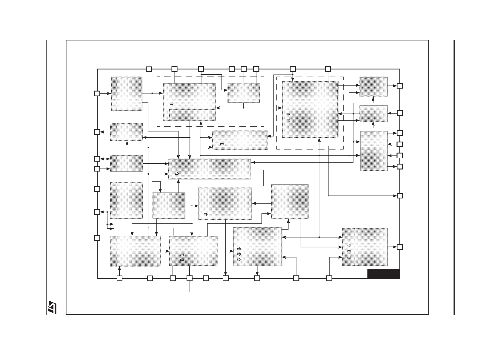
2 - BLOCK DIAGRAM
TDA9115
H/HVSyn
HLckVBk
SDA
SCL
Vcc
RefOut
GND
HGND
7
HPosF
10
HPLL1F
9
R0
HOscF
C0
4
6
8
HFly
12
H-sync
1
detection
Polarity
handling
Phase/frequency
comparator
Horizontal position
Lock detection
3
V-blank
H-lock
31
30
29
13
27
I2C Bus
interface
Supply
supervision
Reference
generation
Internal
ref.
V-sync detection
Input selection
Polarity handling
V-sync
extraction
& detection
Vertical oscillator
2
C Bus registers
I
: Functions controlled via I2C Bus
V-dynamic
correction
(focus, bright.)
VDyCor amplitude
with AGC
S-correction
C-correction
Horizontal
VCO
PLL1
H-moiré controller
H-moiré amplitude
V-ramp control
Tracking EHT
Vertical size
Vertical position
Vertical moiré
Phase comparator
Phase shifter
H duty controller
Pin cushion asymm.
Parallelogram
Geometry
tracking
HPLL2C
5
PLL2
H-drive
buffer
Safety
processor
B+
DC/DC
converter
controller
EW generator
H size
Pin cushion
Keystone
26
25
28
16
15
14
11
24
HOut
XRay
BOut
BISense
BRegIn
BComp
HMoiré
EWOut
2
VSyn
21
VGND
19
VOscF
20 22
VAGCCap
VCap
32
VDyCor
23
VOut
18
VEHTIn
17
HEHTIn
TDA9115
TDA9115
3 - PIN FUNCTION REFERENCE
Pin Name Function
1 H/HVSyn TTL compatible Horizontal /Horizontal and Vertical Sync. input
2 VSyn TTL compatible Vertical Sync. input
3 HLckVBk Horizontal PLL1 Lock detection andVertical early Blanking composite output
4 HOscF High Horizontal Oscillator sawtooth threshold level Filter input
5 HPLL2C Horizontal PLL2 loop Capacitive filter input
6 CO Horizontal Oscillator Capacitor input
7 HGND Horizontal section GrouND
8 RO Horizontal Oscillator Resistor input
9 HPLL1F Horizontal PLL1 loop Filter input
10 HPosF Horizontal Position Filter and soft-start time constant capacitor input
11 HMoiré Horizontal Moiré cancellation output
12 HFly Horizontal Flyback input
13 RefOut Reference voltage Output
14 BComp B+ DC/DC error amplifier (Comparator) output
15 BRegIn Regulation feedback Input of the B+ DC/DC converter controller
16 BISense B+ DC/DC converter current (I) Sense input
17 HEHTIn Input for compensation of Horizontal amplitude versus EHT variation
18 VEHTIn Input for compensation of Vertical amplitude versus EHT variation
19 VOscF Vertical Oscillator sawtooth low threshold Filter (capacitor to be connected to VGND)
20 VAGCCap Input for storage Capacitor for Automatic Gain Control loop in Vertical oscillator
21 VGND Vertical section GrouND
22 VCap Vertical sawtooth generator Capacitor
23 VOut Vertical deflection drive Output for a DC-coupled output stage
24 EWOut E/WOutput
25 XRay X-Ray protection input
26 HOut Horizontal drive Output
27 GND Main GrouND
28 BOut B+ DC/DC converter controller Output
29 Vcc Supply voltage
30 SCL I
31 SDA I
32 VDyCor Vertical Dynamic Correction output
2
C bus Serial CLock Input
2
C bus Serial DAta input/output
5/45
TDA9115
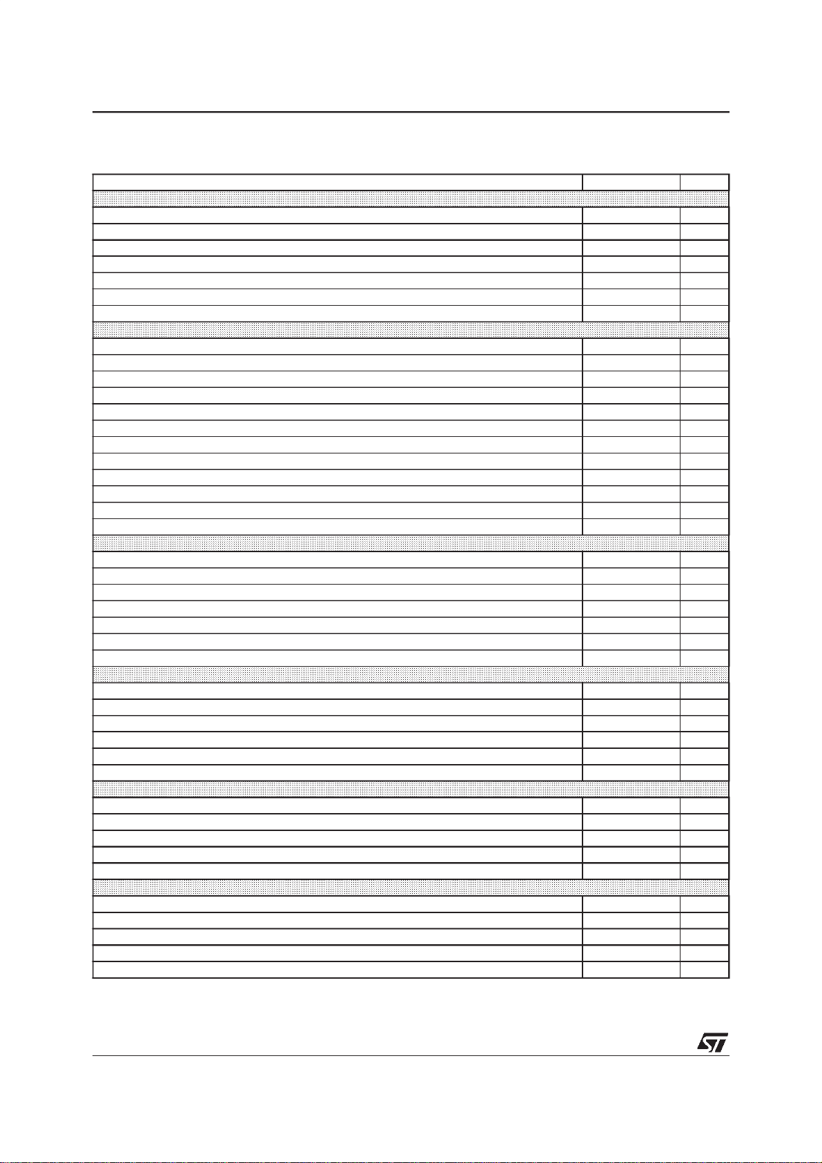
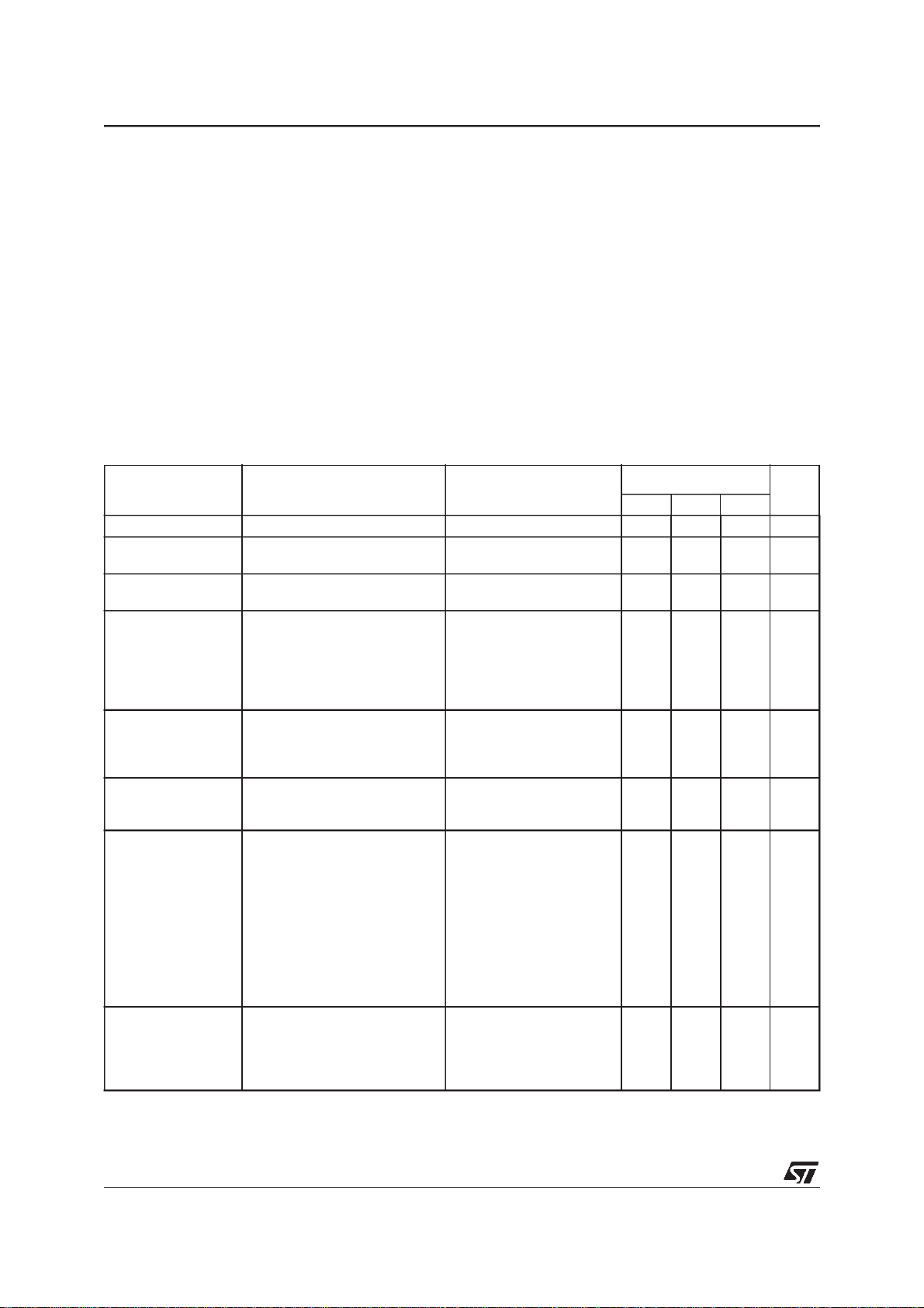
4 - QUICK REFERENCE DATA
Characteristic Value Unit
General
Package SDIP 32
Supply voltage 12 V
Supply current 55 mA
Application category Low-end
Means of control/Maximum clock frequency I
EW drive Yes
DC/DC convertor controller Yes
Horizontal section
Frequency range 15 to 150 kHz
Autosync frequency ratio (can be enlarged in application) 4.28
Positive/Negative polarity of horizontal sync signal/Automatic adaptation Yes/Yes/Yes
Duty cycle of the drive signal 48 %
Position adjustment range with respect toH period ±11 %
Soft start/Soft stop feature Yes/Yes
Hardware/Software PLL lock indication Yes/No
Parallelogram Yes
Pin cushion asymmetry correction (also called Side pin balance) Yes
Top/Bottom/Common corner asymmetry correction No/No/No
Tracking of asymmetry corrections with vertical size & position Yes
Horizontal moiré cancellation (ext.) for Combined/Separated architecture Yes/Yes
Vertical section
Frequency range 35 to 200 Hz
Autosync frequency range (150nF at VCap and 470nF at VAGCCap) 50 to 180 Hz
Positive/Negative polarity of vertical sync signal/Automatic adaptation Yes/Yes/Yes
S-correction/C-correction/Super-flat tube characteristic Yes/Yes/Yes
Vertical size/Vertical position adjustment Yes/Yes
Vertical moiré cancellation (internal) Yes
Vertical breathing compensation Yes
EW section
Pin cushion correction Yes
Keystone correction Yes
Top/Bottom/Common corner correction No/No/No
Horizontal size adjustment Yes
Tracking of EW waveform with Frequency/Vertical size & position Yes/Yes
Breathing compensation on EW waveform Yes
Dynamic correction section (dyn. focus, dyn. brightness,...)
Vertical dynamic correction output VDyCor Yes
Horizontal dynamic correction output No
Composite HV dynamic correction output No
Tracking of horizontal waveform with Horizontal size/EHT No/No
Tracking of vertical waveform with V. size & position Yes
DC/DC controller section
Step-up/Step-down conversion mode Yes/Yes
Internal/External sawtooth configuration No/Yes
Bus-controlled output voltage No
Soft start/Soft stop feature Yes/Yes
Positive(N-MOS)/Negative(P-MOS) polarity of BOut signal Yes/Yes
2
C Bus/400 kHz
6/45
TDA9115
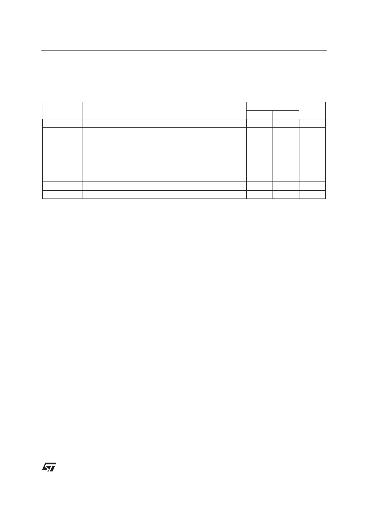
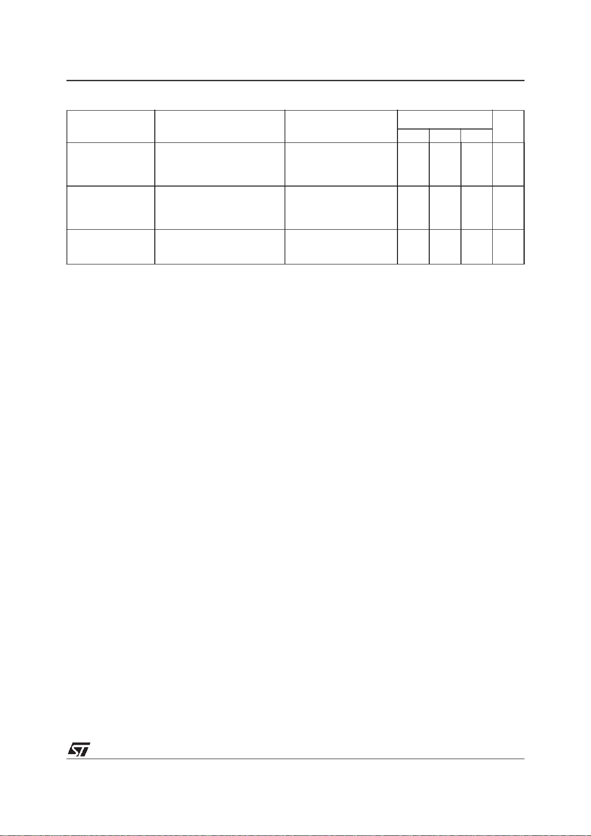
5 - ABSOLUTE MAXIMUM RATINGS
All voltages are given with respect to ground.
Currents flowing from the device (sourced)are signed negative. Currents flowing tothe device aresigned
positive.
Symbol Parameter
V
CC
Supply voltage (pin Vcc) -0.4 13.5 V
Pins HEHTIn, VEHTIn, XRay, HOut, BOut
Pins H/HVSyn, VSyn, SCL, SDA
V
(pin)
Pins HLckVBk, CO, RO, HPLL1F, HPosF, HMoiré, BRegIn, BISense, VAGCCap, VCap, VDyCor, HOscF, VOscF
Pin HPLL2C
Pin HFly
V
T
ESD
stg
T
j
ESD susceptibility
(human body model: discharge of 100pF through 1.5kΩ) -2000 2000 V
Storage temperature -40 150 °C
Junction temperature 150 °C
Value
Min Max
V
V
5.5
V
RefO
RefO
V
RefO
CC
-0.4
-0.4
-0.4
-0.4
-0.4
Unit
V
V
V
/2
V
V
7/45
TDA9115
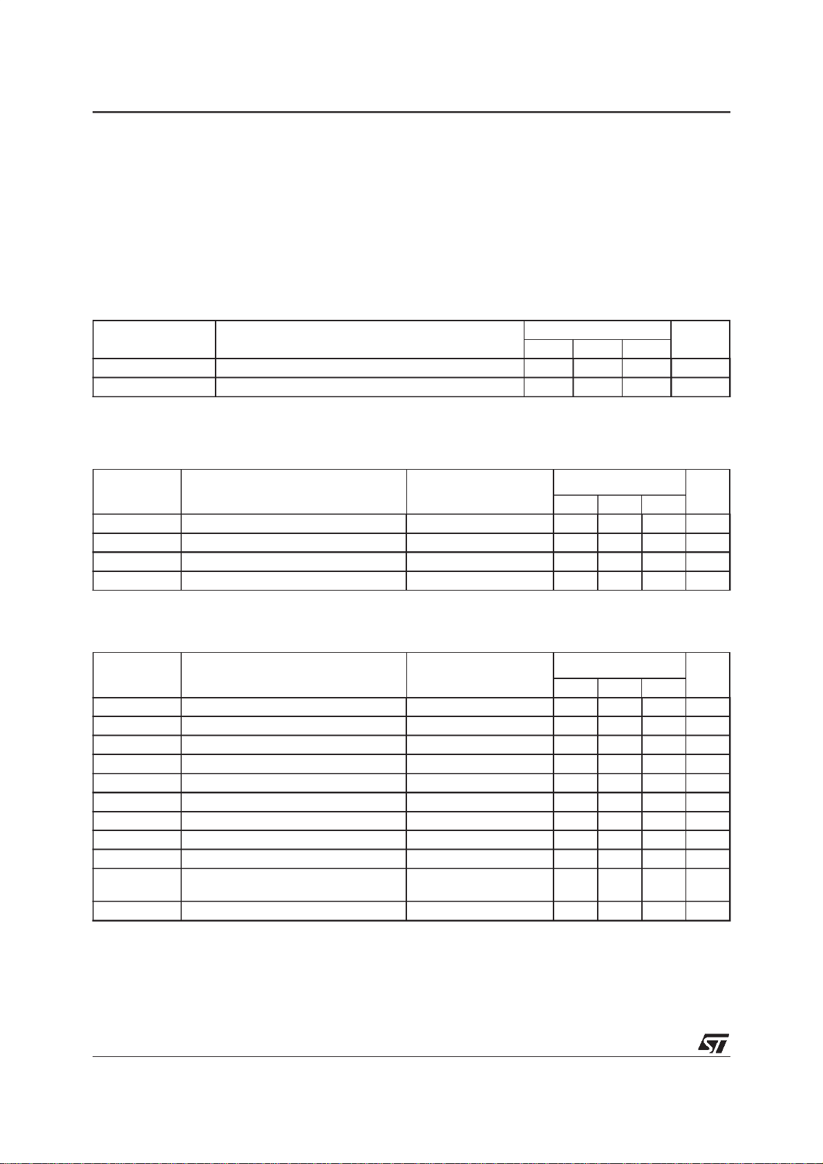
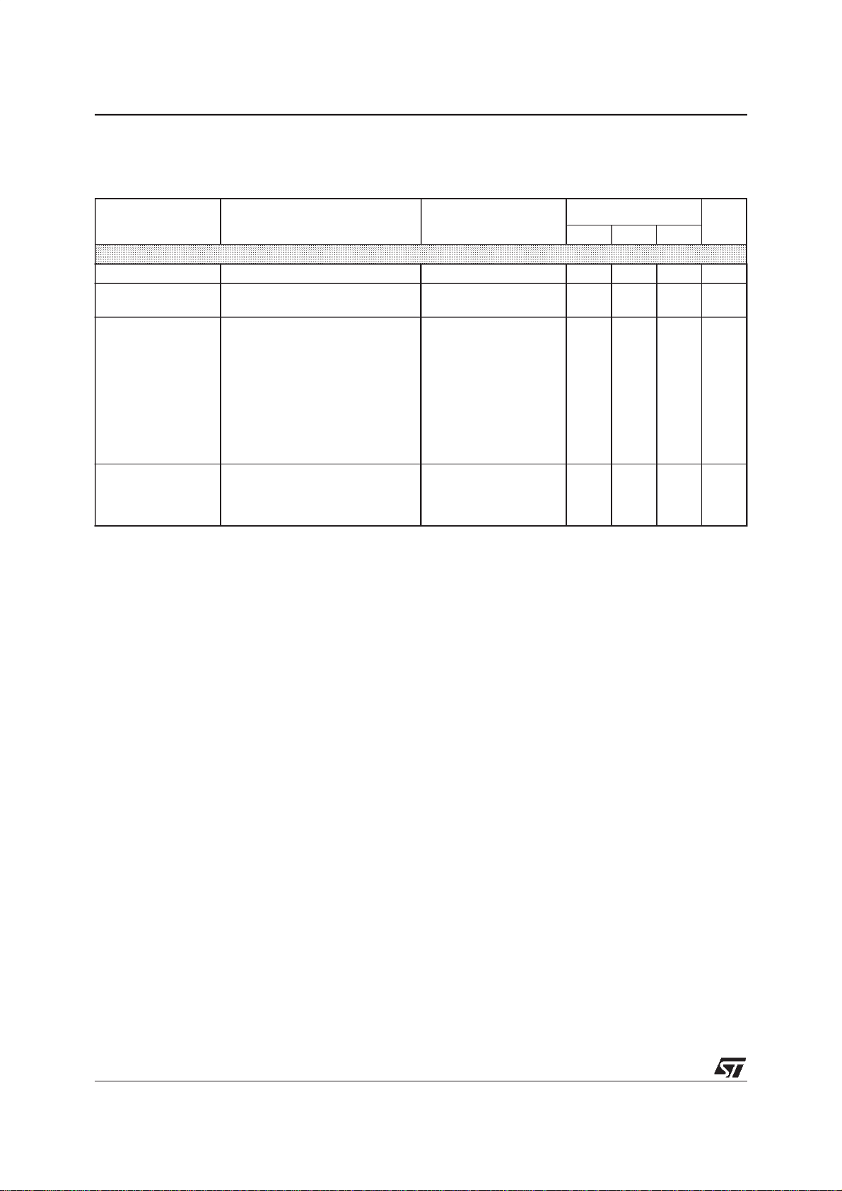
6 - ELECTRICAL PARAMETERS AND OPERATING CONDITIONS
Medium (middle) value of an I2C Bus control or adjustment register composed of bits D0, D1,...,Dn isthe
one having Dn at ”1” and all other bits at ”0”. Minimum value is the one with all bits at 0, maximum value
is the one with all at ”1”.
Currents flowing from the device (sourced)are signed negative. Currents flowing tothe device aresigned
positive.
THis period of horizontal deflection.
6.1 THERMAL DATA
Symbol Parameter
T
R
amb
th(j-a)
Operating ambient temperature 0 70 °C
Junction-ambience thermal resistance 65 °C/W
6.2 SUPPLY AND REFERENCE VOLTAGES
T
=25°C
amb
Symbol Parameter Test Conditions
V
V
I
RefO
CC
I
CC
RefO
Supply voltage at Vcc pin 10.8 12 13.2 V
Supply current to Vcc pin VCC=12V 55 mA
Reference output voltage at RefOut pin VCC=12V,I
Current sourced by RefOutoutput -5 0 mA
6.3 SYNCHRONIZATION INPUTS
Vcc = 12V, T
Symbol Parameter Test Conditions
V
LoH/HVSyn
V
HiH/HVSyn
V
LoVSyn
V
HiVSyn
R
PdSyn
t
PulseHSyn
t
PulseHSyn/TH
t
PulseVSyn
t
PulseVSyn/TV
t
extrV/TH
t
HPolDet
=25°C
amb
LOW level voltage on H/HVSyn 0 0.8 V
HIGH level voltage on H/HVSyn 2.2 5 V
LOW level voltage on VSyn 0 0.8 V
HIGH level voltage on VSyn 2.2 5 V
Internal pull-down on H/HVSyn, VSyn 100 175 250 kΩ
H sync. pulse duration on H/HVSyn pin 0.5 µs
Proportion of H sync pulse to H period Pin H/HVSyn 0.2
V sync. pulse duration Pins H/HVSyn, VSyn 0.5 750 µs
Proportion of V sync pulse to V period Pins H/HVSyn, VSyn 0.15
Proportion ofsync pulse length to H peri-
od for extraction as V sync pulse
Pin H/HVSyn,
cap. on pin CO = 820pF
Polarity detection time (after change) Pin H/HVSyn 0.75 ms
Value
Value
Min. Typ. Max.
= -2mA 7.4 8 8.6 V
RefO
Value
Min. Typ. Max.
0.21 0.3
Unit
Units
Units
8/45
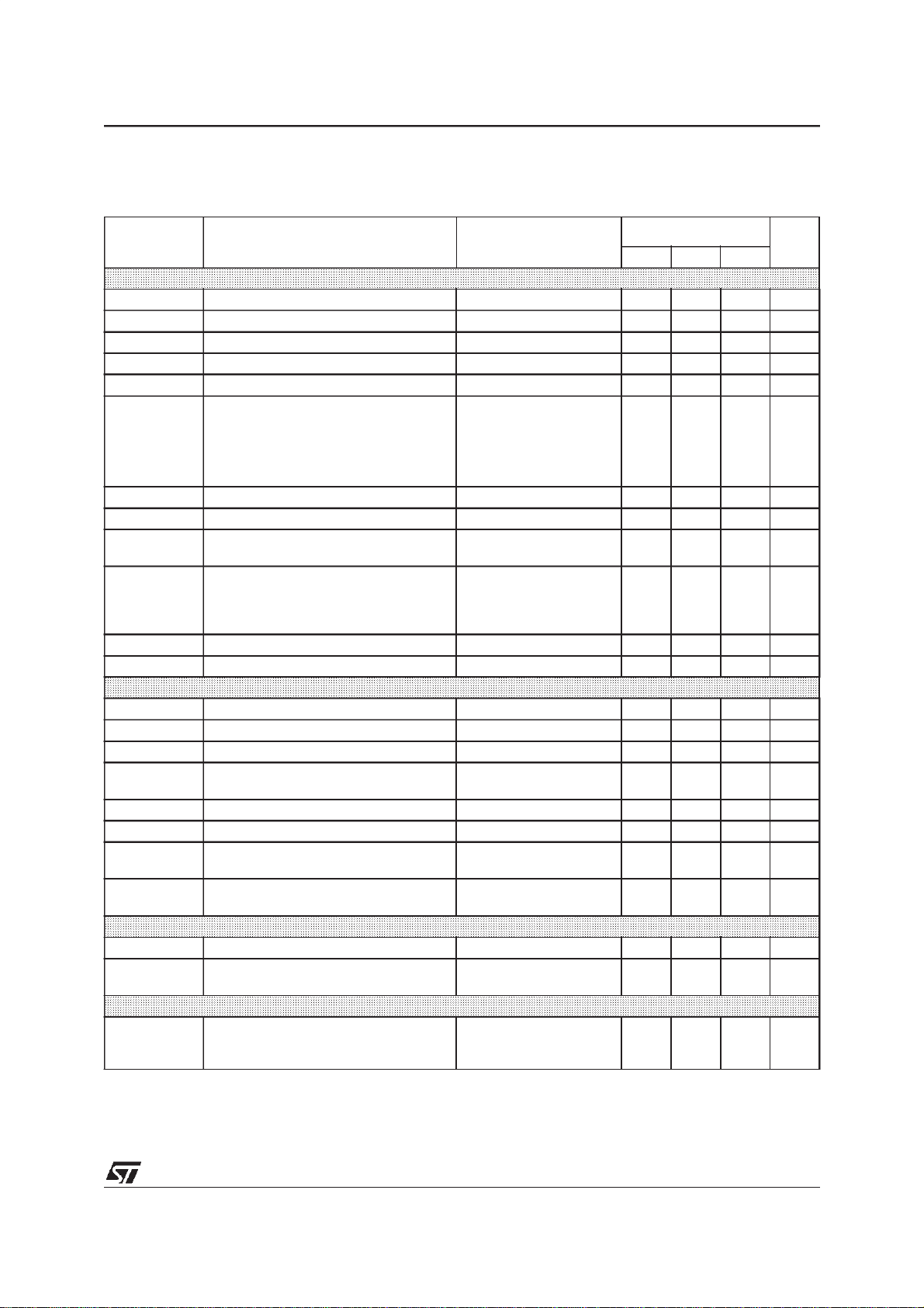
6.4 HORIZONTAL SECTION
TDA9115
Vcc = 12V, T
amb
=25°C
Symbol Parameter Test Conditions
PLL1
I
RO
C
CO
f
HO
f
HO(0)
f
HOCapt
∆
f
HO 0()
-----------------------------
f
HO 0()
∆f
/∆V
HO
V
HO
V
HOThrfr
V
HPosF
Current load on RO pin 1.5 mA
Capacitance on CO pin 390 pF
Frequency of hor. oscillator 150 kHz
Free-running frequency of hor. oscill.
Hor. PLL1 capture frequency
(4)
Temperature drift of free-running freq.
(1)
RRO=5.23kΩ,CCO=820pF 27 28.5 29.9 kHz
f
= 28.5kHz 29 122 kHz
HO(0)
(3)
T∆⋅
Average horizontal oscillator sensitivity f
HO
H. oscill. control voltage on pin HPLL1F V
Threshold on H. oscill. control voltage on
HPLL1F pin for tracking of EW with freq.
Control voltage on HPosF pin
= 28.5kHz 19.6 kHz/V
HO(0)
=8V 1.4 6.0 V
RefO
V
=8V 5.0 V
RefO
HPOS
(Sad01):
11111111b
10000000b
00000000b
V
HOThrLo
V
HOThrHi
Bottom of hor. oscillator sawtooth
Top of hor. oscillator sawtooth
(6)
(6)
PLL2
(6)
(2)
V
(HFly)>VThrHFly
No PLL2 phase modulation
(5)
(5)
Null asym. correction 0 %
Null asym. correction 44 %
R
In(HFly)
I
InHFly
V
ThrHFly
V
S(0)
V
BotHPLL2C
V
TopHPLL2C
(min)/T
t
ph
(max)/T
t
ph
Input impedance on HFly input
Current into HFly input At top of H flyback pulse 5 mA
Voltage threshold on HFly input 0.6 0.7 V
H flyback lock middle point
Low clamping voltage on HPLL2C pin
High clamping voltage on HPLL2C pin
Min. advance of H-drive OFF before
H
middle of H flyback
Max. advance of H-drive OFF before
H
middle of H flyback
(7)
(8)
H-drive output on pin HOut
I
HOut
t
Hoff/TH
Current into HOut output Output driven LOW 30 mA
Duty cycle of H-drive signal
Soft-start/Soft-stopvalue
Picture geometry corrections through PLL1 & PLL2
HPOS
(Sad01):
11111111b
00000000b
t
Hph/TH
H-flyback (center) static phase vs. sync
signal (via PLL1), see Figure 7
Value
Units
Min. Typ. Max.
-150 ppm/°C
2.60
3.30
3.85
2.8
3.4
4.0
3.05
3.55
4.15
1.6 V
6.4 V
300 500 700 Ω
4.0 V
1.6 V
3.75 4.0 4.25 V
48
85
+11
-11
V
V
V
%
%
%
%
9/45

TDA9115
Symbol Parameter Test Conditions
Value
Units
Min. Typ. Max.
PCAC
(Sad11h) full span
t
PCAC/TH
t
ParalC/TH
Contribution of pin cushion asymmetry
correction to phase of H-drive vs. static
phase (via PLL2), measured in corners
Contribution of parallelogram correction
to phase of H-drive vs. static phase (via
PLL2), measured in corners
(9)
(9
VPOS
VSIZE
VSIZE
VSIZE
PARAL
VPOS
VSIZE
VSIZE
VSIZE
VPOS
VSIZE
at medium
at minimum
at medium
at maximum
(Sad12h) fullspan
at medium
at minimum
at medium
at maximum
at max. or min.
at minimum
±1.0
±1.8
±2.8
±1.75
±2.2
±2.8
±1.75
%
%
%
%
%
%
%
Note 1: Frequency at no sync signal condition. For correct operation, the frequency of the sync signal applied must
always be higher than the free-running frequency. The application must consider the spread of values of real
electrical components in R
the free-running frequency is f
and CCOpositions so as to always meet this condition. Theformula to calculate
RO
=0.12125/(RROCCO)
HO(0)
Note 2: Base of NPN transistor with emitter to ground is internally connected on pin HFly through a series resistance of
about 500Ω and a resistance to ground of about 20kΩ.
Note 3: Evaluated and figured out during the device qualification phase. Informative. Not tested on every single unit.
Note 4: This capture range can be enlarged by external circuitry.
Note 5: The voltage on HPLL2C pin corresponds to immediate phase of leading edge of H-drive signal on HOut pin with
respect to internal horizontal oscillator sawtooth. It must be between the two clamping levels given. Voltage
equal to one of the clamping values indicates a marginal operation of PLL2 or non-locked state.
Note 6: Internal threshold. See Figure 7.
Note 7: Thet
(min)/THparameter is fixed by the application. For correct operation of asymmetry corrections through
ph
dynamic phase modulation, this minimum must be increased bymaximum of the total dynamic phase required
in the direction leading to bending of corners to the left. Marginal situation is indicated by reach of V
TopHPLL2C
high clamping level by waveform on pin HPLL2C. Also refer to Note 5 and Figure 7.
Note 8: Thet
(max)/THparameter is fixed by the application. For correct operation of asymmetry corrections through
ph
dynamic phase modulation, this maximum must be reduced by maximum of thetotal dynamic phase required in
the direction leading to bending of corners to the right. Marginal situation is indicated by reach of V
BotHPLL2C
low clamping level by waveform on pin HPLL2C. Also refer to Note 5 and Figure 7 .
Note 9: All other dynamic phase corrections of picture asymmetry set to their neutral (medium) positions.
10/45

6.5 VERTICAL SECTION
TDA9115
VCC= 12V,T
Symbol Parameter Test Conditions
amb
=25°C
Value
Units
Min. Typ. Max.
AGC-controlled vertical oscillator sawtooth; V
R
L(VAGCCap)
V
VOB
V
VOT
t
VODis
f
VO(0)
f
VOCapt
V
∆
VOdev
---------------------------------
V
VOamp
V
∆
--------------------------------
∆
V
--------------------------------
-----------------------------------------
V
VOampfVO
VOS cor–
V
VOamp
VOC cor–
V
VOamp
V
∆
16()
VOamp
∆⋅
Ext. load resistance on
VAGCCap pin
Sawtooth bottom voltage on
VCap pin
(10)
(11)
Sawtooth top voltage on VCap
pin
Sawtooth Discharge time C
Free-running frequency C
AGC loop capture frequency C
Sawtooth non-linearity
(12)
S-correction range
C-correction range
Frequency drift of sawtooth
amplitude
(17)(18)
Vertical output drive signal (on pin VOut);V
V
mid(VOut)
V
amp
V
offVOut
I
VOut
V
VEHT
V
∆
amp
----------------------------------------- -
∆⋅
V
ampVVEHT
Middle point on VOut sawtooth
Amplitude of VOut sawtooth
(peak-to-peak voltage)
Level on VOutpin at V-drive ”off” I2Cbit VOutEn at 0 3.8 V
Current delivered by VOut out-
put
Control input voltage range on
VEHTIn pin
Breathing compensation
RefO
=8V
RefO
∆V
amp/Vamp
No load on VOscF pin
AGC loop stabilized
V sync present
No V sync
VCap
VCap
VCap
AGC loop stabilized,
AGC loop stabilized,
tVR=1/4 T
tVR=3/4 T
AGC loop stabilized,
tVR=1/2 T
CCOR
x0000000b
x1000000b
x1111111b
AGC loop stabilized
f
VOCapt
=8V
VPOS
x0000000b
x1000000b
x1111111b 3.65
VSIZE
x0000000b
x1000000b
x1111111b 3.5
V
VEHT>VRefO
V
VEHT
(R=∞) ≤1% 65 MΩ
(11)
1.8 1.9 2.0 V
5
4.9
V
V
=150nF 80 µs
=150nF 100 Hz
=150nF 50 185 Hz
(15)
VR
VR
(15)
VR
(Sad0A):
(min)≤f
VO≤fVOCapt
(12)
(13)
(14)
(max)
0.5 %
-5
+5
-3
0
+3
200
ppm/Hz
%
%
%
%
%
(Sad08):
3.2
3.5
3.8
3.3 V
V
V
(Sad07):
2.25
3.0
3.75
2.5 V
V
V
-5 5 mA
(min)≤V
VEHT≤VRefO
1 V
0
2.5
RefO
V
%/V
%/V
Note 10: Value of acceptable cumulated parasitic load resistance due tohumidity, AGC storage capacitor leakage, etc.,
for less than 1% of V
amp
change.
11/45
TDA9115
Note 11: The threshold for V
influence the value of V
is generated internally and routed to VOscF pin. Any DC current on this pin will
VOB
VOB
.
Note 12: Maximum of deviation from an ideally linear sawtooth ramp at null
CCOR
(Sad0A at x1000000b). The same rate applies to V-drive signal on VOut pin.
SCOR
Note 13: Maximum
Note 14: Null
Note 15:”t
SCOR
” istime from thebeginning of vertical ramp of V-drive signal on VOut pin.”TVR” isduration of this ramp, see
VR
(Sad09 at x1111111b), null
(Sad09 at x0000000b).
CCOR
(Sad0A at x1000000b).
chapter TYPICAL OUTPUT WAVEFORMSand Figure 19.
Note 16: V
VOamp
= V
VOT-VVOB
Note 17: The same rate applies to V-drive signal on VOut pin.
Note 18: Informative, not tested on each unit.
6.6 EW DRIVE SECTION
VCC= 12V, T
Symbol Parameter Test Conditions
V
EW
I
EWOut
V
HEHT
V
EW-DC
V
∆
EW DC–
-----------------------------
∆
V
HEH T
V
∆
EW DC–
-------------------------------------
V
EW DC–
V
EW-PCC
V
EW PCC–
--------------------------------------------------------
EW PC C–
tvrTVR=[]
=25°C
amb
Output voltage on EWOut pin 1.8 6.5 V
Current sourced by EWOut out-
put
Control voltage range on HEH-
TIn pin
DC component of the EW-drive
signal on EWOut pin
Breathing compensation on
V
Temperature drift of DC component of the EW-drive signal on
T∆⋅
EWOut pin
Pin cushion correction component of the EW-drive signal on
EWOut pin
tvr0=[]
Tracking of PCC component of
the EW-drive signalwith vertical
position adjustment
EW-DC
(19)(20)(21)(28)
tVR=1/2 T
HSIZE
VR
(Sad10h):
00000000b
10000000b
11111111b
(19)((20)
tVR=1/2 T
V
HEHT>VRefO
V
HEHT
(18)(19)(21)(28)
tVR=1/2T
(19)(21)(22)(23)(24)(28)
VSIZE
PCC
VR
(min)≤V
VR
at maximum
(Sad0C):
x0000000b
x1000000b
x1111111b
Tracking with
PCC
at x1000000b
VSIZE
(Sad07):
x0000000b
x1000000b
(19)(22)(25)(27)(28)
PCC
at x1111111b
VPOS
(Sad08):
x0000000b
x1111111b
SCOR
(15)
(15)
HEHT≤VRefO
(15)
VSIZE
(Sad09 at x0000000b) and null
Value
Min. Typ. Max.
-1.5 0 mA
1 V
2
3.25
4.5
0
-0.125
100 ppm/°C
0
0.7
1.5
:
0.25
0.5
0.52
1.92
RefO
Units
V
V
V
V
V/V
V/V
V
V
V
V
V
12/45
TDA9115
Symbol Parameter Test Conditions
Value
Units
Min. Typ. Max.
Keystone correction component
V
EW-Key
V
∆
-------------------------------------------------------- -
VEWf
-----------------------------------------------------
V
EW AC–
Note 19:
Note 20:
Note 21:
Note 22:
EW
⋅
[]
max
V
∆
EW AC–
V
∆⋅
KEYST
PCC
VPOS
HSIZE
∆
HEHT
at minimum value.
of the EW-drive signal on
EWOut pin
Tracking of EW-drive signal with
horizontal frequency
V
HO
Breathing compensation on
(29)
V
EW-AC
at medium (neutral) value.
at medium (neutral) value.
at minimum value.
Note 23: Defined as difference of (voltage at t
Note 24: Defined as difference of (voltage at t
Note 25:
Note 26: Difference: (voltage at t
VSIZE
at maximum value.
=0) minus (voltage at tVR=TVR).
VR
(30)
=0) minus (voltage at tVR=1/2 TVR).
VR
VR=TVR
(20)(21)(22)(25)(26)(28)
KEYST
(Sad0D):
x0000000b
x1111111b
VHO>V
HOThrfr
VHO(min)≤VHO≤V
(23)(24)
V
HEHT>VRefO
V
(min)
HEHT
HOThrfr
V
≤
HEHT≤VRefO
) minus (voltage at tVR=1/2 TVR).
0.4
-0.4
0
20
0
1.75
Note 27: Ratio ”A/B”of parabola component voltage at tVR=0 versus parabola component voltage at tVR=TVR.
See Figure 2.
Note 28: V
Note 29: V
HEHT>VRefO
EW-AC
, V
VEHT>VRefO
is the sum ofall components other than V
(contribution of PCC and keystone correction).
EW-DC
Note 30: More precisely tracking with voltage on HPLL1F pin which itself depends on frequency at a rate given by
external components on PLL1 pins. V
[fmax] is the value at condition VHO>V
EW
HOThrfr
.
V
V
%/V
%/V
%/V
%/V
13/45
TDA9115
6.7 DYNAMIC CORRECTION OUTPUTS SECTION
VCC= 12V, T
Symbol Parameter Test Conditions
Vertical Dynamic Correction output VDyCor
I
VDyCor
V
VD-DC
IV
VD-V
V
VD V–tvr
------------------------------------------------- -
V
VD V–tvrTVR
Note 31: Ratio ”A/B”of vertical parabola component voltage at tVR=0 versus vertical parabola component voltage at
t
VR=TVR
=25°C
amb
Current sunk from VDyCor output -1.5 -0.1 mA
DC component of the drive signal
on VDyCor output
I
=[]
Amplitude ofV-parabola on VDyCor output
0=[]
Tracking of V-parabola on VDyCor
output with vertical position
.
(21)
(31)
R
L(VDyCor)
VSIZE
at medium
VDC-AMP
xxxxxx00
xxxxxx01
xxxxxx10
xxxxxx11
VDC-AMP
VSIZE
(Sad07):
x0000000b
x1111111b
VDC-AMP
VPOS
(Sad08):
x0000000b
x1111111b
Value
Min. Typ. Max.
=10kΩ 4V
(Sad15h):
0.25
0.50
0.75
1.00
at maximum
0.6
1.6
at maximum
0.52
1.92
Units
V
V
V
V
V
V
14/45

6.8 DC/DC CONTROLLER SECTION
TDA9115
VCC= 12V, T
amb
=25°C
Symbol Parameter Test Conditions
R
B+FB
A
OLG
f
UGBW
I
RI
I
BComp
A
BISense
V
ThrBIsCurr
I
BISense
I
BOut
V
BOSat
V
BReg
Ext. resistance applied between
BComp output and BRegIn input
Open loop gain of error amplifier
on BRegIn input
Unity gain bandwidth of error am-
Low frequency
(18)
plifier on BRegIn input
Bias current delivered by regula-
tion input BRegIn
Output current capability of BComp
output.
Voltage gain on BISense input 3
Threshold voltage on BISense input
corresponding to current limitation
Input current sourcedby BISense input -1 µA
Output current capability of BOut
output
Saturation voltage of the internal output
transistor on BOut
Regulation reference for BRegIn
(33)
voltage
HBOutEn = ”Enable”
HBOutEn = ”Disable”
I
=10mA 0.25 0.35 V
BOut
V
=8V 4.7 4.8 5.0 V
RefO
Delay of BOut “Off-to-On” edge after
t
BTrigDel/TH
middle of flyback pulse, as part of T
(34)
BOutPh = ”0” 16 %
H
(18)
Value
Min. Typ. Max.
5kΩ
100 dB
6 MHz
-0.2 µA
-0.5
(32)
0.5
1.98 2.1 2.22 V
010mA
Units
2.0 mA
mA
Note 32: A current sink is provided by the BComp output while BOut is disabled:
Note 33: Internal reference related to V
. The same values to be found on pin BRegIn, while regulation loop is
RefO
stabilized.
Note 34: Only applies to configuration specified in ”Testconditions” column, i.e. synchronization of BOut “Off-to-On”
edge with horizontal flyback signal. Refer to chapter ”DC/DC controller” for more details.
15/45

TDA9115
6.9 MISCELLANEOUS
VCC= 12V, T
Symbol Parameter Test Conditions
amb
=25°C
Value
Units
Min. Typ. Max.
Vertical blanking and horizontal lock indication composite output HLckVBk
I
SinkLckBk
Sink current to HLckVBk pin
(35)
100 µA
V.blank H.lock
V
OLckBk
Output voltage on HLckVBk output
No Yes
Yes Yes
No No
Yes No
0.1
1.1
5
6
Horizontal moiré canceller
Rext=10kΩ
V
AC-HMoiré
V
DC-HMoiré
H-moiré pulse amplitude on HMoiré pin
HMOIRE
x0000000b
x1111111b
DC level on HMoiré pin Rext=10kΩ 0.1 V
(Sad02):
0.1
2.1
Vertical moiré canceller
V
V-moiré
Amplitude of modulation of V-drive signal on VOut pin by vertical moiré.
VMOIRE
x0000000b
x1111111b
(Sad0Bh):
0
3
mV
mV
Protection functions
V
ThrXRay
t
XRayDelay
V
CCEn
V
CCDis
Input threshold on XRayinput
Delay time between XRay detection
event and protection action
VCCvalue for start of operation at V
ramp-up
VCCvalue for stop of operation at V
ramp-down
(37)
(37)
Control voltages on HPosF pin for Soft start/stop operation
V
HOn
V
BOn
V
HBNorm f
Threshold for start/stop of H-drive signal
Threshold for start/stop of B-drive signal
Threshold for full operational duty cycle
of H-drive and B-drive signals
(36)
CC
CC
(18)
7.65 7.9 8.2 V
2T
H
8.5 V
6.5 V
1V
1.7 V
2.4
Normal operation
V
HPos
Voltage on HPosF pin asfunction of adjustment of
HPOS
register
HPOS
(Sad01)
00000000b
11111111b
3.85
2.60
4.0
2.8
4.15
3.05
Note 35: Current sunk by the pin if the external voltage is higher than one the circuit tries to force.
Note 36: The threshold is equal to actual V
RefO
.
Note 37: In the regions of VCCwhere the device’s operation is disabled, the H-drive, V-drive and B+-drive signals on
2
HOut, VOut and BOut pins, resp., are inhibited, the I
C Bus does not accept any data.
V
V
V
V
V
V
V
V
16/45

7 - TYPICAL OUTPUT WAVEFORMS
Note (38)
Function Sad Pin Byte Waveform Effect on Screen
V
x0000000
Vertical Size 07 VOut
x1111111
amp(min)
V
amp(max)
V
mid(VOut)
V
mid(VOut)
TDA9115
Vertical
Position 08 VOut
S-correction 09 VOut
C-correction 0A VOut
x0000000
x1000000
x1111111
x0000000:
Null
x1111111:
Max.
x0000000
x1000000 :
Null
V
VOamp
V
VOamp
V
VOamp
V
VOamp
V
mid(VOut)
V
VOS-cor
0 1/4T
VR
0 1/2T
V
mid(VOut)
V
mid(VOut)
3/4 T
V
VOC-cor
VR
VRTVR
T
VR
3.5V
3.5V
3.5V
t
VR
t
VR
x1111111
V
VOamp
0 1/2T
V
VOC-cor
VR
T
VR
t
VR
17/45

TDA9115
Function Sad Pin Byte Waveform Effect on Screen
V
amp
(n-1)T
V
amp
(n-1)T
V
EW-DC(min)
V
EW-DC(max)
V
V
0 1/2T
0 1/2T
nT
nT
(n+1)T
V
V
VR
VR
V
V-moiré
(n+1)T
V
t
V
t
T
t
VR
VR
T
VR
t
VR
Vertical moiré
amplitude
0B VOut
Horizontal size 10h EWOut
x0000000:
Null
x1111111:
Max.
00000000
11111111
Keystone
correction
Pin cushion
correction
Parallelogram
correction
Pin cushion
asymmetry
correction
0D EWOut
0C EWOut
12h
Internal
11h
Internal
x0000000
x1111111
x0000000
x1111111
x0000000
x1111111
x0000000
x1111111
V
EW-key
V
EW-key
V
EW-PCC(min)
0 1/2 T
V
EW-PCC(max)
0 1/2 T
t
ParalC(min)
0 1/2T
t
ParalC(max)
0 1/2T
t
PCAC(max)
0 1/2 T
t
PCAC(max)
0 1/2 T
V
EW-DC
V
EW-DC
VR
VR
static phase
VR
static phase
VR
VR
VR
T
VR
T
VR
T
T
T
VR
T
VR
VR
VR
static
H-phase
static
H-phase
t
VR
t
VR
t
VR
t
VR
t
VR
t
VR
18/45

TDA9115
Function Sad Pin Byte Waveform Effect on Screen
VR
VR
VDyCorPo
V
VD-DC
T
t
VR
VR
V
VD-DC
T
VR
t
VR
Application dependent
V
VD-V(max)
Vertical
dynamic
correction
amplitude
15h VDyCor
xxxxxx11
0 1/2 T
V
VD-V(max)
xxxxxx00
0 1/2 T
Note 38: For any H and V correction component of the waveforms on EWOut and VOut pins and for internal waveform
for corrections of H asymmetry,displayed in the table, weight of the other relevant components is nullified
(minimum for parabola, S-correction, medium for keystone, all corner corrections, C-correction, parallelogram,
parabola asymmetry correction, written in corresponding registers).
19/45

TDA9115
8-I2C BUS CONTROL REGISTER MAP
The device slave address is 8C in write mode and 8D in read mode.
Bold weight denotes default value at Power-On-Reset.
I2C Bus data in the adjustment register isbuffered and internally applied withdischarge of the vertical oscillator .
In order to ensure compatibility with future devices, all “Reserved” bits should be set to 0.
SadD7 D6D5D4D3D2D1D0
WRITE MODE (SLAVE ADDRESS = 8C)
00 Reserved
01
02
03 Reserved
04 Reserved
05 Reserved
06
07
08
09 Reserved
0A Reserved
0B Reserved
0C Reserved
0D Reserved
0E Reserved
0F Reserved
10
11 Reserved
12 Reserved
13 Reserved
14 Reserved
15 Reserved
1 000000
HMoiré
1: Separated
0: Combined
BOutPol
0: Type N
BOutPh
0: H-flyback
1: H-drive
EWTrHFr
0: No tracking
1 000000
0000000
1000000
1000000
1000000
1000000
0000000
1000000
1000000
1000000
1000000
HPOS (Horizontal position)
HMOIRE (Horizontal moiré amplitude)
VSIZE (Vertical size)
VPOS (Vertical position)
SCOR (S-correction)
CCOR (C-correction)
VMOIRE (Vertical moiré amplitude)
PCC (Pin cushion correction)
KEYST (Keystone correction)
HSIZE (Horizontal size)
PCAC (Pin cushion asymmetry correction)
PARAL (Parallelogram correction)
Reserved
00
Reserved
Reserved
VDC-AMP
20/45

TDA9115
SadD7 D6D5D4D3D2D1D0
XRayReset
16
0: No effect
1: Reset
17
Note 39: The TV,TH, TVM and THM bits are for testing purposes and must be kept at 0 by application.
TV
0:Off
(39)
Description of I2C Bus switches
Write-to bits
VSyncAuto
1:On
TH
(39)
0:Off
VSyncSel
0:Comp
1:Sep
TVM
0:Off
(39)
00
THM
0: Off
(39)
BOHEdge
0: Falling
PLL1Pump
1: Fast
0: Slow
HBOutEn
0: Disable
PLL1InhEn
1:On
VOutEn
0: Disable
HLockEn
1:On
BlankMode
1: Perm.
Sad02/D7 - HMoiré
Horizontal Moiré characteristics
0: Adaptedto an architecturewith EHTgener-
ated in deflection section
1: Adapted to an architecture with separated
deflection and EHT sections
Sad06/D7 - BOutPol
Polarity of B+ drive signal on BOutpin
0: adapted to N type of power MOS - high
level to make it conductive
1: adaptedto P type ofpower MOS -low level
to make it conductive
Sad07/D7 - BOutPh
Phase of start of B+ drive signal on BOut pin
0: Just after horizontal flyback pulse
1: With one of edges of line drive signal on
HOut pin, selected by BOHEdge bit
Sad08/D7 - EWTrHFr
Tracking of all corrections contained in wave-
form on pin EWOut with Horizontal Frequency
0: Not active
1: Active
Sad16/D2 - PLL1Pump
Horizontal PLL1 charge Pump current
0: Slow PLL1, low current
1: Fast PLL1, high current
Sad16/D5 - VSyncSel
Vertical Synchronization input Selection be-
tween the one extracted from composite HV signal on pin H/HVSyn and the one on pin VSyn.
No effect if VSyncAuto bit is at 1.
0: V.sync extractedfromcomposite signal on
H/HVSyn pin selected
1: V. sync applied on VSyn pin selected
Sad16/D6 - VSyncAuto
Vertical Synchronization input selection Auto-
matic mode. If enabled, the device automatically
selects between the vertical sync extracted from
composite HV signal on pin H/HVSyn and the
one on pin VSyn, based on detection mechanism. If both are present, the one coming first is
kept.
0: Disabled, selection done according to bit
VSyncSel
1: Enabled, the bit VSyncSel has no effect
Sad16/D0 - HLockEn
Enable of output of Horizontal PLL1 Lock/unlock
status signal on pin HLckVBk
0: Disabled, vertical blanking only on the pin
HLckVBk
1: Enabled
Sad16/D1 - PLL1InhEn
Enable of Inhibition of horizontal PLL1 during
extracted vertical synchronization pulse
0: Disabled, PLL1 is never inhibited
1: Enabled
Sad16/D7 - XRayReset
Reset to 0 of XRay effected with ACK bit of I2C
Bus data transfer into register containing the
XRayReset bit.
0: No effect
1: Reset with automatic return of the bit to 0
This bit is not latched, it will return to 0 byitself.
Sad17/D0 - BlankMode
Blanking operation Mode
0: Blanking pulse starting with detection of
vertical synchronization pulse and ending
with end of vertical oscillator discharge
21/45

TDA9115
(startof verticalsawtooth rampon the VOut
pin)
1: Permanentblanking -high blanking level in
composite signal on pin HLckVBk is permanent
Sad17/D1 - VOutEn
Vertical Output Enable
0: Disabled, V
Vertical section)
offVOut
on VOut pin (see 6.5
1: Enabled,verticalramp with vertical position
offset on VOut pin
Sad17/D2 - HBOutEn
Horizontal and B+ Output Enable
0: Disabled, levels corresponding to “power
transistor off”on HOut and BOut pins(high
for HOut, high or low for BOut, depending
on BOutPol bit).
1: Enabled, horizontal deflection drive signal
on HOut pin providing thatit isnotinhibited
by another internal event (activated XRay
protection). B+ drive signal on BOut pin.
Programming the bit to 1 after prior value of 0,
will initiate soft start mechanism of horizontal
drive and of B+ DC/DC convertor
Sad17/D3 - BOHEdge
Selection of Edge of Horizontal drive signal to
phase B+ drive Output signal on BOut pin. Only
applies if the bit BOutPh is set to 1, otherwise
BOHEdge has no effect.
0: Falling edge
1: Rising edge
Sad17/D4,D5,D6,D7 - THM, TVM, TH, TV
Test bits. They must be kept at 0 level by application S/W.
22/45

TDA9115
9 - OPERATING DESCRIPTION
9.1 SUPPLY AND CONTROL
9.1.1 Power supply and voltage references
The device is designed for a typical value of power
supply voltage of 12 V.
In order to avoid erratic operation of the circuit at
power supply ramp-up or ramp-down, the value of
VCCis monitored. See Figure 1 and electrical
specifications. At switch-on, the device enters a
“normal operation” as the supply voltage exceeds
V
V
ence, a hysteresis to bridge potential noise. Outside the “normal operation”, the signals on HOut,
BOut and VOut outputs are inhibited and the I2C
bus interface is inactive (high impedance on SDA,
SCL pins, no ACK), all I2C bus control registers
being reset to their default values (see chapter I2C
BUS CONTROL REGISTER MAP on page 20).
Figure 1. Supply voltage monitoring
Internal thresholds in all parts of the circuit are derived from a common internal reference supply
V
tering against ground as well as for external use
with load currents limited to I
necessary to minimize interference in output signals, causing adverse effects like e.g. jitter.
9.1.2 I2C Bus Control
The I2C bus isa 2 linebi-directional serial communication bus introduced by Philips. For its general
and stays there until it decreases below
CCEn
. The two thresholds provide, by theirdiffer-
CCDis
V
V
(Vcc)
that is lead out to RefOut pin for external fil-
RefO
CC
V
CCEn
Disabled Disabled
hysteresis
Normal operation
RefO
. The filtering is
V
CCDis
t
description, refer to corresponding Philips I2C bus
specification.
This device is an I2C bus slave, compatible with
fast (400kHz) I2C bus protocol, with write mode
slave address of 8C. Integrators are employed at
the SCL (Serial Clock) input andat the inputbuffer
of theSDA (Serial Data)input/output tofilter off the
spikes of up to 50ns.
The device supports multiple data byte messages
(with automatic incrementation of the I2C bus subaddress) as well as repeated Start Condition for
I2C bus subaddress change inside the I2Cbus
messages. All I2C bus registers with specified I2C
bus subaddress are of WRITE ONLY type.
For the I2C buscontrol register map, refer to chapter I2C BUS CONTROL REGISTER MAP on
page 20.
9.2 SYNC. PROCESSOR
9.2.1 Synchronization signals
The device has two inputs for TTL-levelsynchronization signals, both with hysteresis to avoid erratic
detection and with a pull-down resistor. On H/
HVSyn input, pure horizontal or composite horizontal/vertical signal is accepted. On VSyn input,
only pure vertical sync. signal is accepted. Both
positive and negative polarities may be applied on
either input, see Figure 2. Polarity detector and
programmable inverter are provided on each of
the twoinputs. The signal applied on H/HVSyn pin,
after polarity treatment, is directly lead to horizontal part andto an extractor of vertical sync. pulses,
working on principle of integration, see Figure 3.
The vertical sync. signal applied to thevertical deflection processor is selected between the signal
extracted from the composite signal on H/HVSyn
input and the one applied on VSyn input. The selector is controlled by VSyncSel I2C bus bit.
Besides the polarity detection, the device is capable of detecting the presence of sync. signals on
each of the inputs and at the output of vertical
sync. extractor.The device isequipped withan automatic mode (switched on or off by VSyncAuto
I2C bus bit) that uses the detection information.
23/45

TDA9115
Figure 2. Horizontal sync signal
Positive
T
H
Negative
t
PulseHSyn
Figure 3. Extraction of V-sync signal from H/V-sync signal
H/V-sync
T
Internal
Integration
Extracted
V-sync
H
9.2.2 Automatic sync. selection mode
I2C bus bit VSyncAuto is set to 1. In this mode, the
device itself controls the I2C bus bits switching the
polarity inverters and the vertical sync. signal selector (VSyncSel), using the information provided
by detection circuitry. If both extracted and pure
vertical sync. signals are present, the one already
selected is maintained. No intervention of the
MCU is necessary.
t
PulseHsyn
t
extrV
nent phase offset. On the screen, this offset results inthe change ofhorizontal position of thepicture. The loop, by tuning the VCO accordingly,
gets and maintains in coincidence the rising edge
of inputsync. signal withsignal REF1, which is derived from the VCO ramp by a comparator with
threshold adjustable through
trol. The coincidence is identified and flagged by
lock detection circuit on pin HLckVBk .
The charge pump provides positive and negative
9.3 HORIZONTAL SECTION
9.3.1 General
The horizontal section consists of two PLLs with
various adjustments and corrections, working on
horizontal deflection frequency, then phase shifting and output driving circuitry providing H-drive
signal on HOut pin. Input signal to the horizontal
section is output of the polarity inverter on H/
HVSyn input. The device ensures automatically
that this polarity be always positive.
9.3.2 PLL1
The PLL1 block diagram is in Figure 5. It consists
of a voltage controlled oscillator (VCO), a shaper
with adjustablethreshold, acharge pump withinhibition circuit, a frequency and phase comparator
and timing circuitry. The goal of the PLL1 is to
make theVCO ramp signal match in frequency the
sync. signal and to lock this ramp in phase to the
sync. signal, with a possibility to adjust a perma-
currents charging the external loop filter on HPosF
pin. The loop is independent of the trailing edge of
sync. signal and only locksto its leading edge. By
design, the PLL1 does not suffer from any dead
band even while locked. The speed of the PLL1
depends on the current value provided by the
charge pump. While notlocked, the current is very
low, to slow down the changes of VCO frequency
and thus protect the external power components
at sync. signal change. In locked state, the currents are much higher, two different values being
selectable via PLL1Pump I2C bus bit to provide a
mean to control the PLL1 speed by S/W. Lower
values make the PLL1 slower, but more stable.
Higher values make it faster and less stable. In
general, the PLL1 speed should be higher for high
deflection frequencies. The response speed and
stability (jitter level) depends on the choice of external components making up the loop filter. A
“CRC” filter is generally used (see Figure 4 on
page 25).
HPOS
I2C bus con-
24/45

TDA9115
Figure 4. H-PLL1 filter configuration
HPLL1F
9
R
2
C
2
C
1
The PLL1 is internally inhibited during extracted
vertical sync. pulse (if any) to avoid taking into account missing or wrong pulses on the phase comparator. Inhibitionis obtained byforcing the charge
Figure 5. Horizontal PLL1 block diagram
PLL1
H/HVSyn
1
Sync
Polarity
INPUT
INTERFACE
Extracted
V-sync
LOCK
DETECTOR
COMP
REF1
High
Low
pump output to high impedance state. The inhibition mechanism can be disabled through
PLL1Pump I2C bus bit.
The Figure 7, in its upper part, shows the position
of the VCO ramp signal in relation to input sync.
pulse for three different positions of adjustment of
horizontal position control
PLL1InhEn
2
V-sync (extracted)
C)
PLL
INHIBITION
HPosF
10
SHAPER
Lock
Status
2
(pin & I
CHARGE
PUMP
PLL1Pump
2
(I
C)
(I
C)
HPOS
HPLL1F
9
HPOS
(I
.
R0 C0
86
2
C)
HOscF
4
VCO
HOSC
Figure 6. Horizontal oscillator (VCO) schematic diagram
(PLL1 filter)
HPLL1F
from charge pump
I
0
I
2
V
HO
9
+
-
RO
0
4I
8
0
V
HOThrHi
V
6
4
HOThrLo
CO
HOscF
+
-
-
+
V
HOThrHi
V
HOThrLo
RS
Flip-Flop
VCO discharge
control
25/45

TDA9115
9.3.3 Voltage controlled oscillator
The VCO makes part of both PLL1 and PLL2
loops, being an “output” to PLL1 and “input” to
PLL2. It delivers a linear sawtooth. Figure 6 explains itsprinciple of operation. The linears are obtained bycharging anddischarging an external capacitor on pinCO, with currents proportional to the
current forced through an external resistor on pin
RO, which itself depends on the input tuning voltage VHO(filtered charge pump output). The rising
and falling linears are limited by V
V
HOThrHi
thresholds filtered through HOscF pin.
HOThrLo
and
At no signal condition, the VHOtuning voltage is
clamped to its minimum (see chapter ELECTRICAL PARAMETERS AND OPERATING CONDITIONS, part horizontal section), which corresponds to the free-running VCO frequency f
HO(0)
Refer to Note1 for theformula to calculate this frequency usingexternal components values.The ratio between the frequency corresponding to maximum VHOand the one corresponding to minimum
VHO(free-running frequency) is about 4.5. This
range can easily be increased in the application.
The PLL1 can onlylock to input frequenciesfalling
inside these two limits.
9.3.4 PLL2
The goal of the PLL2 is, by means of phasing the
signal driving the power deflection transistor, to
lock the middle of the horizontal flyback to a certain threshold of the VCO sawtooth. This internal
threshold is affected by geometry phase corrections, like e.g., parallelogram. The PLL2 is much
faster thanPLL1 to be ableto follow the dynamism
of thisphase modulation.The PLL2control current
(see Figure 7) issignificantly increased during discharge of vertical oscillator (during vertical retrace
period) to be able to make up for the difference of
dynamic phase at the bottom and at the top of the
picture. The PLL2 control current is integrated on
the external filter on pin HPLL2C to obtain
smoothed voltage, used, in comparison with VCO
ramp, asa threshold for H-drive risingedge generation.
As both leading and trailing edges of the H-drive
signal in the Figure 7 must fallinside therising part
of the VCO ramp, an optimum middle position of
the threshold has been found to provide enough
margin forhorizontal outputtransistor storage time
as well as for the trailing edge of H-drive signal
with maximum duty cycle. Yet, the constraints
thereof must be taken into account while considering the application frequency range and H-flyback
duration. The Figure 7 also shows regions for rising and fallingedges of theH-drive signal onHOut
pin. As it is forced high during the H-flyback pulse
and lowduring theVCO discharge period, no edge
during these two events takes effect.
The flyback input configuration is in Figure 8.
9.3.5 Dynamic PLL2 phase control
.
The dynamic phase control of PLL2 is used to
compensate for picture asymmetry versus vertical
axis across the middle of the picture. It is done by
modulating the phase of the horizontal deflection
with respect to the incoming video (synchronization). Inside the device, the threshold V
pared with the VCO ramp, the PLL2 locking the
middle of H-flyback to the moment of their match.
The dynamic phase is obtained by modulation of
the threshold by correction waveforms. Refer to
Figure 12 and to chapter TYPICAL OUTPUT
WAVEFORMS. The correction waveforms have
no effect in vertical middle of the screen (for middle verticalposition).As they are summed, their effect onthe phase tends to reachmaximum span at
top and bottom of the picture. As all the components of the resulting correction waveform (linear
for parallelogram correction and parabola of 2nd
order for Pin cushion asymmetry correction) are
generated from the outputvertical deflection drive
waveform, they both track with real vertical amplitude and position (including breathing compensation), thus being fixed on the screen. Refer to I2C
BUS CONTROL REGISTER MAP on page 20 for
details on I2C bus controls.
S(0)
iscom-
26/45

TDA9115
Figure 7. Horizontal timing diagram
t
H-sync
(polarized)
PLL1 lock
REF1
(internal)
V
HPosF
max.
H-Osc
(VCO)
H-flyback
PLL2
control
control
current
H-drive
(on HOut)
H-drive
region
H-drive
region
t
: HOTstorage time
S
med.
min.
ON
t
ph(max)
Hph
min max
t
S
+
V
S(0)
7/8T
H
T
H
V
ThrHFly
-
OFF
t
Hoff
forced high forced low
inhibited
ON
V
HOThrHi
V
HPOS
(I2C)
max.
med.
min.
HOThrLo
PLL1
Figure 8. HFly input configuration
~500Ω
HFly
12
~20kΩ
int.ext.
GND
9.3.6 Output section
The H-drive signal is inhibited (high level) during
flyback pulse, and also when VCCis too low, when
I2C bus bit HBOutEn is set to 0 (default position).
The PLL2 is followed by a rapid phase shifting
which accepts the signal from H-moiré canceller
(see sub chapter Horizontal moiré cancellation on
page 27)
The output stage consists of a NPN bipolar transistor, the collector of which is routed to HOut pin
(see Figure 9).
Figure 9. HOut configuration
26
HOut
int. ext.
Non-conductive state of HOT (Horizontal Output
Transistor) must correspond to non-conductive
state of the device output transistor.
9.3.7 Soft-start and soft-stop on H-drive
PLL2
The soft-start and soft-stop procedure is carried
out at each switch-on or switch-off of the H-drive
signal via HBOutEn I2C bus bit to protect external
power components.By itssecond function, the external capacitor on pin HPosF is used to time out
this procedure, during which the duty cycle of Hdrive signal starts at its maximum (“t
Hoff/TH
start/stop” in electrical specifications) and slowly
decreases. This is controlled by voltage on pin
HPosF. See Figure 10 and sub chapter Safety
functions on page 33.
9.3.8 Horizontal moiré cancellation
The horizontalmoiré cancelleris intended toblur a
potential beat between the horizontal video pixel
period and the CRT pixel width, which causes visible moiré patterns in the picture.
On pinHMoiré, it generates a square line-synchronized waveform with amplitude adjustable through
HMOIRE
I2C bus control.
The behaviour of horizontal moiré is to be optimised fordifferent deflectiondesign configurations
using HMoiré I2C bus bit.This bit is to be kept at0
for common architecture (B+ and EHT common
regulation) and at 1 forseparated architecture (B+
and EHT each regulated separately).
for soft
27/45

TDA9115
Figure 10. Control of HOut and BOut at start/stop at nominal V
V
VOB
HPosMin
Normal operation
threshold.
VOT
VAGCCap. Onthe screen,this corresponds tostabilized vertical size of picture. After a change of
frequency on the sync. input, thestabilization time
depends on the frequency difference and on the
capacitor value. The lower its value, the shorter
the stabilization time, but on the other hand, the
lower the loop stability. A practical compromise is
a capacitance of 470nF. The leakage current of
this capacitor results in difference in amplitudebetween low and high frequencies. The higher its
parallel resistance R
ference.
When the synchronization pulse is not present, the
charging current is fixed. As a consequence, the
free-running frequency f
value of the capacitor on pin VCap. It can be
roughly calculated using the following formula
V
(HPosF)
V
HPosMax
V
HBNorm
V
BOn
V
HOn
HOut
H-duty cycle
BOut (positive)
B-duty cycle
Soft start
Start
HOut
Start
BOut
9.4 VERTICAL SECTION
9.4.1 General
The goal of the vertical section is to drive vertical
deflection output stage. It delivers a sawtooth
waveform with an amplitude independent of deflection frequency, on whichvertical geometry corrections of C- and S-type are superimposed (see
chapter TYPICAL OUTPUT WAVEFORMS).
Block diagram is inFigure 11. The sawtooth is obtained by charging an external capacitor on pin
VCap with controlled current and by discharging it
via transistor Q1. This is controlled by the CONTROLLER. The charging starts when the voltage
across the capacitor drops below V
The discharging starts either when it exceeds V
threshold or a short time after arrival of synchronization pulse. This time is necessary for the AGC
loop to sample the voltage at the top of the sawtooth. The V
reference is routed out onto VO-
VOB
f
VO(0)
=
scF pin in order to allow for further filtration.
The charging current influences amplitude and
shape of the sawtooth. Just before the discharge,
the voltage across the capacitor on pin VCap is
sampled and stored on a storage capacitor connected on pinVAGCCap. During the following vertical period, this voltage is compared to internal
reference REF (V
ling thegain of the transconductance amplifierpro-
), the result thereof control-
VOT
viding the charging current. Speed of this AGC
loop depends on the storage capacitance on pin
The frequency range in which the AGC loop can
regulate the amplitude also depends on this capacitor.
The C- and S-corrections of shape serve to compensate for the vertical deflection system non-linearity. They are controlled via
I2C bus controls.
Shape-corrected sawtooth with regulated amplitude is lead to amplitude control stage. The dis-
cc
150nF
C
(VCap)
minimum value
HPOS
(I2C)
range
maximum value
Soft stop
Stop
BOut
Stop
HOut
L(VAGCCap)
VO(0)
.
100Hz
t
100%
0%
, the lower this dif-
only depends on the
CCOR
and
SCOR
28/45

TDA9115
charge exponential is replaced by V
VOB
level,
which, under control of the CONTROLLER, creates a rapid falling edge and a flat part before beginning of new ramp. Mean value of the waveform
output on pin VOut is adjusted by means of
I2C bus control, its amplitude through
VPOS
VSIZE
I2C
bus control. Vertical moiré is superimposed.
The biasing voltage for external DC-coupled verti-
cal power amplifier is to be derived from V
RefO
voltage provided on pin RefOut, usinga resistor divider, this to ensure the same temperature drift of
mean (DC) levels on both differential inputsand to
Figure 11. Vertical section block diagram
OSC
Cap.
Discharge
VSyn
2
Synchro
Polarity
Controller
compensate for spread of V
value (and so
RefO
mean output value) between particular devices.
9.4.2 Vertical moiré
To blur the interaction of deflection lines with CRT
mask grid pitch that can generate moiré pattern,
the picture position is to bealternated at frame frequency. For this purpose, a square waveform at
half-frame frequency is superimposed on the output waveform’s DC value. Its amplitude is adjustable through
VCap
22
Q1
VMOIRE
Chargecurrent
Sampling
I2C bus control,.
Transconductanceamplifier
REF
20
VAGCCap
Sampling
Capacitance
S-correction
SCOR
CCOR
CCOR
(I2C)
2
C)
(I
19
VOscF
9.5 EW DRIVE SECTION
The goal of the EW drive section is to provide, on
pin EWOut, a waveform which, used by an external DC-coupled power stage, serves to compensate for those geometry errors of the picture that
are symmetric versus vertical axis across the middle of the picture.
The waveform consistsof an adjustable DCvalue,
corresponding tohorizontal size,a parabola of 2nd
order for “pin cushion” correction and a linear for
“keystone” correction. All of them are adjustable
via I2C bus, see I2C BUS CONTROL REGISTER
MAP on page 20.
C-correction
18
23
VEHTIn
VOut
V
VOB
VMOIRE
VPOS
sawtooth
discharge
(I2C)
(I2C)
VSIZE
(I2C)
Refer to Figure 12, Figure 13 and to chapter TYPICAL OUTPUT WAVEFORMS. The correction
waveforms have no effect in the vertical middle of
the screen (if the
VPOS
control is adjusted to its
medium value). As they are summed, the resulting
waveform tends to reach its maximum span at top
and bottom of the picture. The voltage at the
EWOut is top and bottom limited (see parameter
VEW). According to Figure 13, especially the bot-
tom limitation seems to be critical for maximum
horizontal size (minimum DC). Actually it is not
critical sincethe parabola componentmust always
be applied. As all the components of the resulting
correction waveform are generated from the out-
29/45

TDA9115
put vertical deflection drive waveform, they all
track with real vertical amplitude and position (including breathing compensation), thus being fixed
vertically on the screen. They are also affected by
C- andS-corrections. The sum of components other than DC is affected by value in
HSIZE
I2Cbus
control in reversedsense. Refer to electrical specifications for value. The DC value, adjusted via
HSIZE
control, is also affected by voltage on HEHTIn input, thus providing a horizontal breathing
compensation (see electrical specifications for value). The resulting waveform is conditionally multiplied with voltage on HPLL1F, which depends on
frequency. Refer to electrical specifications for value and moreprecision. This tracking with frequency provides a rough compensation of variation of
picture geometry with frequency and allows to fix
the adjustmentranges of I2C buscontrols throughout the operating range of horizontal frequencies.
It can be switched off by EWTrHFr I2C bus bit (off
by default).
The EW waveform signal is buffered by an NPN
emitter follower, the emitter of which is directly
routed to EWOut output,with nointernal resistorto
ground. It is to be biased externally.
Figure 12. Geometric corrections’ schematic diagram
Controls:
one-quadrant
two-quadrant
V
mid(VOut)
2
VOut
23
VDC-AMP
2
C)
(I
VDyCor
32
Vertical ramp
PCC
KEYST
2
(I
C)
2
C)
(I
PCAC
PARAL
Tracking
HEHTIn/HSize
Tracking
with Hor
Frequency
(I2C)
To horizontal
dyn. phase control
(I2C)
24
HSize
17
HEHTIn
EWOut
30/45

Figure 13. EWOut output waveforms
V
(EWOut)
V
EW-Key
V
EW-PCC
V
EW-DC
non-authorized region
V
EW
HSIZE
m
ini
m
edium
m
m
i
ax
m
VEW(min)
(max)
(I2C)
um
um
TDA9115
operating range
EW
V
Keystone PCC
alonealone
V
V
(VCap)
(VCap)
T
0
0
T
0
0
VR
VR
9.6 DYNAMIC CORRECTION OUTPUT
SECTION
9.6.1 Vertical Dynamic Correction output
VDyCor
A parabola at vertical deflection frequencyis available onpin VDyCor. Its amplitude isadjustable via
VDC-AMP
I2C bus control. It tracks with real vertical amplitude and position (including breathing
compensation). It is also affected by C- and S-corrections.
The use of this correction waveform is up to the
application (e.g. dynamic focus).
9.7 DC/DC CONTROLLER SECTION
The section is designed to control a switch-mode
DC/DC converter. A switch-mode DC/DC convertor generates a DC voltage from a DC voltage of
different value (higher or lower) with little power
losses. The DC/DC controller is synchronized to
Breathing
compensation
V
(min)
V
(min)
HEHT
HEHT
Vertical sawtooth
T
T
VR
VR
t
t
VR
VR
horizontal deflection frequency to minimize potential interference into the picture.
Its operation is similar to that of standardUC3842.
The schematic diagram of the DC/DC controller is
in Figure 14. The BOut output controls an external
switching circuit (a MOS transistor) delivering
pulses synchronized on horizontal deflection frequency, the phase of which depends on I2C bus
configuration, seethe table at theend of this chapter. Their duration depends on feedbackprovided
to the circuit, generally a copy of DC/DC converter
output voltage and a copy of current passing
through theDC/DC converter circuitry (e.g. current
through external power component). The polarity
of the output can becontrolled byBOutPol I2C bus
bit. ANPN transistor open-collectoris routedout to
the BOut pin.
During the operation, a sawtooth is to be found on
pin BISense, generated externally by the application. According to BOutPh I2C bus bit, the R-S flipflop is set either at H-drive signal edge (rising or
falling, depending on BOHEdge I2C bus bit), or a
V
V
RefO
RefO
V
(HEHT)
31/45

TDA9115
certain delay (t
BTrigDel/TH
back. The output is set On at the end of a short
pulse generated by the monostable trigger.
Timing of reset of the R-S flip-flop affects duty cycle of the output square signal and so the energy
transferred from DC/DC converter input to its output. A reset edge is provided by comparator C2 if
the voltage on pin BISense exceeds the internal
threshold V
ThrBIsCurr
tation if a voltage proportional to the current
through the power component or deflection stage
) after middle of H-fly-
. This represents current limi-
compared, and the reset signal generated by the
comparator C1. The error amplifier amplifies (with
a factor defined by external components) the difference between the input voltage proportional to
DC/DC convertoroutput voltage and internal reference V
Both step-up (DC/DC converter output voltage
higher than its input voltage) and step-down (output voltage lower than input) are possible.
DC/DC controller Off-to-On edge timing
is available on pin BISense. This threshold is affected by thevoltage onpin HPosF, which rises at
soft start and descends at soft stop. This ensures
self-contained soft control of duty cycle of the output signalon pinBOut. Referto Figure 10. Another
condition for the reset of the R-S flip-flop, OR-ed
with the one described before, is that the voltage
on pin BISense exceeds the voltage VC1, which
depends on the voltage applied on input BISense
of the error amplifier O1. The two voltages are
Figure 14. DC/DC converter controller block diagram
BOHEdge
2
C)
BOutPh
2
C)
(I
Monostable
~500ns
(I
H-drive edge
H-flyback
(+delay)
.
BReg
BOutPh
(Sad07/
D7)
BOHEdge
(Sad17/
D3)
0 don’t care Middle of H-flyback plus t
1 0 Falling edge of H-drive signal
1 1 Rising edge of H-drive signal
I1
Timing of Off-to-On transition
on BOut output
V
CC
BTrigDel
Feedback
V
BReg
BRegIn
BComp
V
ThrBIsCurr
HPosF
+
O1
-
Soft start
2R
R
BIsense
I2
N type
V
C1
-
C1
+
-
C2
+
S
Q
R
HBOutEn
XRayAlarm
P type
BOutPol
(I
2
(I
C)
I3
2
C)
BOut
32/45

TDA9115
9.8 MISCELLANEOUS
9.8.1 Safety functions
The safety functions comprise supply voltage
monitoring with appropriate actions, soft start and
soft stop features on H-drive and B-drive signals
on HOut and BOut outputs and X-ray protection.
For supply voltage supervision, refer to paragraph
Power supply and voltage references on page 23
and Figure 1. A schematic diagram putting together all safety functions and composite PLL1 lock
and V-blanking indication is in Figure 15.
9.8.2 Soft start and soft stop functions
For softstart and soft stop features for H-drive and
B-drive signal, refer to paragraph Soft-start and
soft-stop on H-drive on page 27 and sub chapterDC/DC CONTROLLER SECTION on page 31, respectively. See also the Figure 10. Regardless
why the H-drive or B-drive signal are switched on
or off (I2C bus command, power up or down, X-ray
protection), the signals always phase-in and
phase-out in the way drawn in the figure, the first
to phase-inand last to phase-outbeing theH-drive
signal, which isto better protect the power stages
at abrupt changes like switch-on and off. The timing of phase-in and phase-out only depends on
the capacitance connected to HPosF pin which is
virtually unlimited for thisfunction. Yet it has adual
function (see paragraph PLL1 on page 24), so a
compromise thereof is to be found.
9.8.3 X-ray protection
The X-ray protection is activatedif the voltage level onXRay inputexceeds V
consequence, the H-drive and B-drive signals on
ThrXRay
threshold. As a
HOut and BOut outputs are inhibited (switched off)
after a 2-horizontal deflection line delay provided
to avoid erratic excessive X-ray condition detection at short parasitic spikes.
This protectionis latched;it may be reset eitherby
VCCdrop or by I2C bus bit XRayReset (see chap-
ter I2C BUS CONTROL REGISTER MAP on
page 20).
33/45

TDA9115
Figure 15. Safety functions - block diagram
HBOutEn
2
I
C
V
CCEn
V
CCDis
29
Vcc
XRayReset
2
C
I
XRay
25
V
ThrXRay
HFly
12
V
ThrHFly
VOutEn
2
C
I
VCCsupervision
+
_
+
_
H-VCO
+
discharge
control
_
In Out
:2
R
RSQ
HPosF
(timing)
10
SOFT START
& STOP
B-drive inhibit
H-drive inhibit
H-drive inhibition
(overrule)
V-drive inhibition
BlankMode
2
C
I
HlockEn
2
C
I
H-lock detector
V-sawtooth
discharge
V-sync
B-drive inhibition
L1=No blank/blank level
Σ
HLckVbk
L3=L1+L2
3
L2=H-lock/unlock level
R
Q
S
2
C3I2C bit
I
Int. signal
Pin
34/45

TDA9115
9.8.4 Composite output HLckVBk
The composite output HLckVBk provides, at the
same time, information about lock state of PLL1
and early vertical blanking pulse. As both signals
have two logical levels, a four level signal is used
to define the combination of the two. Schematic diagram putting together all safety functions and
composite PLL1 lock and V-blanking indication is
in Figure 15, the combinations, their respective
levels andthe HLckVBk configuration in Figure 16.
The early vertical blanking pulse is obtained by a
logic combination of vertical synchronization pulse
and pulse corresponding to vertical oscillator discharge. Thecombination correspondsto the drawing in Figure 16.The blanking pulse is started with
Figure 16. Levels on HLckVBk composite output
V
CC
HLckVBk3
I
SinkLckBlk
the leading edge of any of the two signals, whichever comes first. The blanking pulse is ended with
the trailing edge of vertical oscillator discharge
pulse. The device has no information about the
vertical retrace time. Therefore, it does not cover,
by the blanking pulse, the whole vertical retrace
period. By means of BlankMode I2C bus bit, when
at 1 (default), the blanking level (one of two according to PLL1 status) is made available on the
HLckVBk permanently. The permanent blanking,
irrespective of the BlankMode I2C bus bit, is also
provided if the supply voltage is low (under V
or V
tive or if the V-drive signal is disabled by VOutEn
thresholds), if the X-ray protection is ac-
CCDis
CCEn
I2C bus bit.
L1 - No blank/blank level
L2 - H-lock/unlock level
L1
+L2
(H)
(H)
L1
+L2
(L)
(H)
V
OLckBlk
V-early blanking
HPLL1 locked
L1
(L)
Yes
+L2
(L)
L1
+L2
(H)
(L)
YesNo
Yes No
No Yes
No
35/45

TDA9115
Figure 17. Ground layout recommendations
1
2
TDA9115
3
4
5
6
7
8
9
10
11
12
13
14
15
32
31
30
29
28
27
26
25
24
23
22
21
20
19
18
16 17
General Ground
36/45

10 - INTERNAL SCHEMATICS
Figure 18.
TDA9115
Figure 21.
Pins 1-2
H/HVSyn
VSyn
Figure 19.
HLckVBkl
5V
3
200Ω
12V
13
RefOut
5
HPLL2C
Figure 22.
12V
6
C0
12V
RefOut
13
RefOut
13
Figure 20.
HOSCF
Pin 4
12V
Pin 13
Figure 23.
8
R0
12V
RefOut
13
37/45

TDA9115
Figure 24.
HPLL1F
Figure 25.
HPosF
Figure 27.
9
HFly
12V
12
Figure 28.
RefOut
12V
10
BComp
14
Figure 26.
HMoiré
38/45
12V 5V 5V
11
Figure 29.
BRegIn
12V
15

TDA9115
Figure 30.
BISense
16
Figure 31.
18 VEHTIn
17
HEHTIn
12V
12V
Figure 33.
VAGCCap
Figure 34.
12V
22
VCap
12V
20
Figure 32.
VOSCF
19
12V
Pin 13
Figure 35.
23
VOut
12V
39/45

TDA9115
Figure 36.
24 EWOut
32 VDyCor
Figure 37.
XRay
Figure 39.
12V
30 SCL
31SDA
12V
25
Figure 38.
26 HOut
28 BOut
40/45
12V

11 - PACKAGE MECHANICAL DATA
32 PINS - PLASTIC SHRINK
TDA9115
E
E1
A2
B1B
D
32 17
1
Dimensions
A 3.556 3.759 5.080 0.140 0.148 0.200
A1 0.508 0.020
A2 3.048 3.556 4.572 0.120 0.140 0.180
B 0.356 0.457 0.584 0.014 0.018 0.023
B1 0.762 1.016 1.397 0.030 0.040 0.055
C .203 0.254 0.356 0.008 0.010 0.014
D 27.43 27.94 28.45 1.080 1.100 1.120
E 9.906 10.41 11.05 0.390 0.410 0.435
E1 7.620 8.890 9.398 0.300 0.350 0.370
e 1.778 0.070
eA 10.16 0.400
eB 12.70 0.500
L 2.540 3.048 3.810 0.100 0.120 0.150
Min. Typ. Max. Min. Typ. Max.
Millimeters Inches
e
16
A
A1
L
Stand-off
C
eA
eB
41/45

TDA9115
12 - GLOSSARY
AC Alternate Current
ACK ACKnowledge bit of I2C-bus transfer
AGC Automatic Gain Control
COMP COMParator
CRT Cathode Ray Tube
DC Direct Current
EHT Extra High Voltage
EW East-West
H/W HardWare
HOT Horizontal Output Transistor
I2CInter-Integrated Circuit
IIC Inter-Integrated Circuit
MCU Micro-Controller Unit
NAND Negated AND (logic operation)
NPN Negative-Positive-Negative
OSC OSCillator
PLL Phase-Locked Loop
PNP Positive-Negative-Positive
REF REFerence
RS, R-S Reset-Set
S/W SoftWare
TTL Transistor Transistor Logic
VCO Voltage-Controlled Oscillator
42/45

Revision follow-up
PRODUCT PREVIEW
June 2000 version 2.0
Document created (issued from TDA9112)
Work on figures and text; version finalized and displayed on Intranet.
July 2000 version 2.1
Sentence modified in first page : The internal sync processor.;.” replaced by :”the device only requires..;”
Bloc diagram : addition of Hsize under E/W correction
Quick Reference Data: Addition of parrallelogram
Register Map: subaddress 08: 0:No tracking
Few corrections in text.
PRELIMINARY DATA
September 2000 version3:0
Uniformity in the writing of cross references for notes.
In internal schematics, correction of figure for pin 11.
In bloc diagram: the line between PLL2 and HMoiré controller has been deleted
In Horizontal Moiré Cancellation: 1 sentence changed
VDC AMP replaced by VDC-AMP
In electrical parameters:
∆V
Addition of V
HMoiré
becomes ∆V
DC-HMoiré
AC-HMoiré
,.
January 11, 2001 version 3.1
page 6: value for autosync frequency ratio replaced : 4.28 instead of 4.5 previously.
April 19, 2001 version 3.2
page 16 Section 6.9 .Vtrh-XRay: new values 7.65 min, 7.9 typ., 8.2 max.
DATASHEET
July 18, 2001 version 4.0
Section 9.4.1 right column”The higher its value,...” ---> ”The lower its value”
Section 9.5 .”...at the vertical middle...” ---> ”...in the vertical middle...”
Section 6.6 : addition of[fmax] toparameter ”∆VEW/VEW[fmax].∆VHO” .andchanged its
value to 20
Note 28: added: “VEW[fmax] is the value at condition VHO>VHOThrfr”.
Section 6.4 : addition of min and max valuesfor V
Section 6.5 addition ofmin and max values for V
VOB
and V
HPosF
+ correction of typ. value
TopHPLL2C
2

Section 6.8 addition of min and max values for V
for V
BOSat
Section 6.9 addition of min and max values for V
ThrBlsCurr
HPos
and V
, max value added
BReg
Section 9.4 “stabilizing time” changed to “stabilization time” (twice)
Section 6.9 : max valuesfor vertical moiré cancellers moved to typ. values

TDA9115
Information furnished isbelieved tobe accurate and reliable. However, STMicroelectronics assumes no responsibility for the consequences of use of such information nor for any infringement of patents or other rights of
third parties which may result from its use. No license is granted by implication or otherwise under any patent
or patent rights of STMicroelectronics. Specifications mentioned in this publication are subject to change without notice. This publication supersedes and replaces all information previously supplied. STMicroelectronics
products are not authorized for use as critical components in life support devices or systems without the express written approval of STMicroelectronics.
The ST logo is a registered trademark of STMicroelectronics
2001 STMicroelectronics - All Rights Reserved.
Purchase of I
components inan I
2
C Components by STMicroelectronics conveys a license under thePhilips I2C Patent. Rights touse these
2
C system is granted provided that the system conforms tothe I2C Standard Specification as defined
by Philips.
STMicroelectronics Group of Companies
Australia - Brazil -China -Finland - France -Germany - Hong Kong - India - Italy - Japan - Malaysia -Malta -Morocco -
Singapore - Spain Sweden - Switzerland - United Kingdom - U.S.A.
http://www.st.com
45/45
 Loading...