

TDA9110
LOW-COST DEFLECTIONPROCESSOR
FOR MULTISYNC MONITORS
PRODUCT PREVIEW
HORIZONTAL
.
EXTREMELY LOWJITTERLEVEL
.
SELF-ADAPTATIVE
.
DUALPLL CONCEPT
.
150kHzMAXIMUM FREQUENCY
.
X-RAYPROTECTION INPUT
.
I2C CONTROLS : HORIZONTAL DUTY-CYCLE,
H-POSITION
VERTICAL
.
VERTICALRAMPGENERATOR
.
50 TO 165Hz AGC LOOP
.
GEOMETRYTRACKING WITH V-POS & AMP
.
I2C CONTROLS:
V-AMP,V-POS, S-CORR, C-CORR
.
DC BREATHINGCOMPENSATION
2
I
C GEOMETRYCORRECTIONS
.
VERTICALPARABOLAGENERATOR
(Pincushion,Keystone)
.
HORIZONTALSIZE CONTROL (Amplitude)
.
HORIZONTALDYNAMICPHASE
(SidePin Balance & Parallelogram)
.
HORIZONTALAND VERTICALDYNAMIC FOCUS (Horizontal Focus Amplitude, Horizontal
FocusSymmetry, VerticalFocus Amplitude)
GENERAL
.
SYNCHROPROCESSOR
.
12V SUPPLYVOLTAGE
.
8V REFERENCE VOLTAGE
.
HOR.& VERT. LOCKUNLOCK OUTPUTS
.
READ/WRITE I2C INTERFACE
.
HORIZONTALAND VERTICALMOIRE
DESCRIPTION
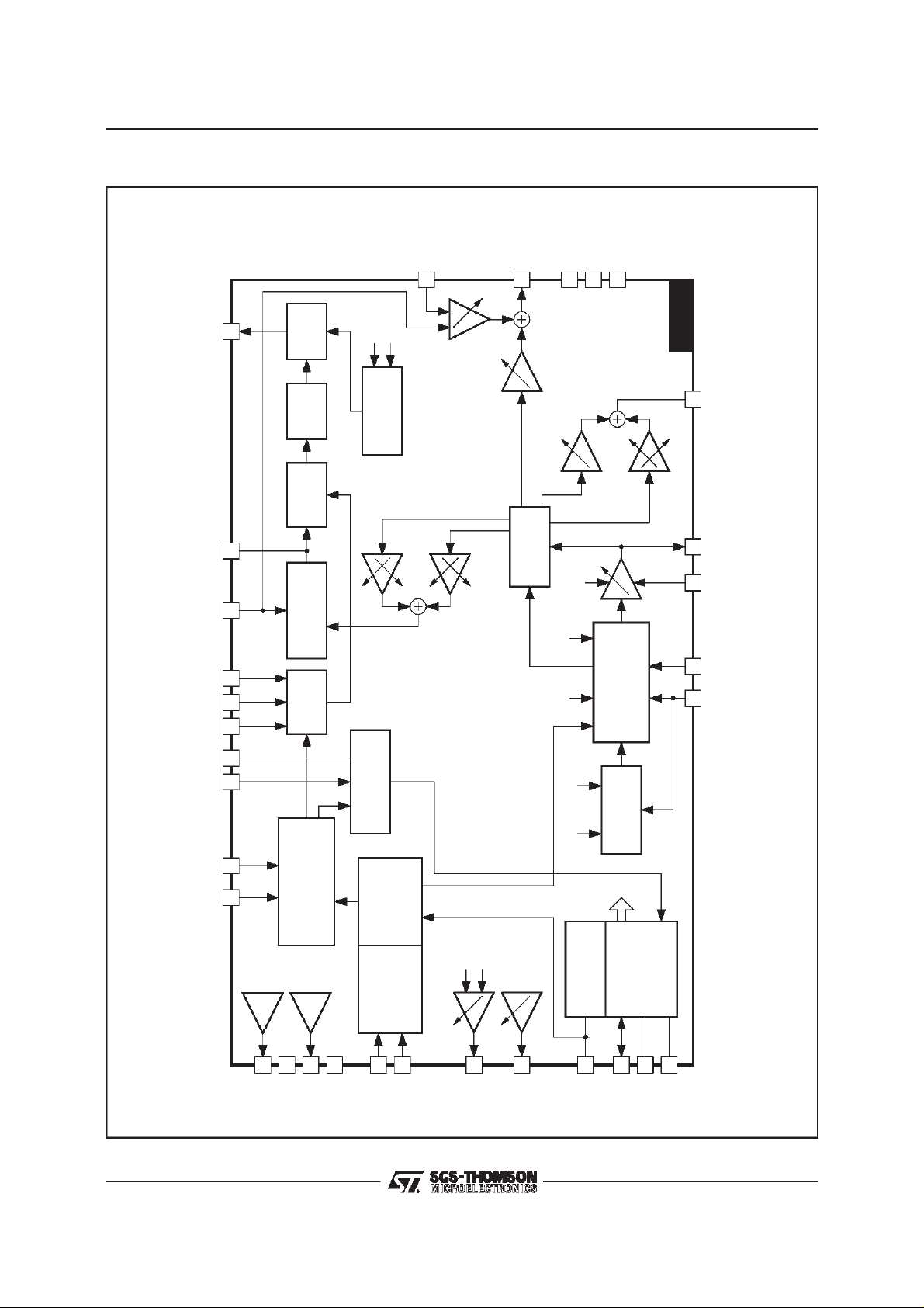
The TDA9110 is a monolithicintegrated circuit assembledin 32-pin shrunkdual in line plasticpackage.This IC controlsall thefunctionsrelatedto the
horizontal and vertical deflection in multimode or
multi-frequencycomputerdisplaymonitors.
Theinternalsynchroprocessor, combinedwith the
very powerful geometrycorrectionblock make the
TDA9110suitablefor very high performancemonitorswith very few externalcomponents.
Thehorizontal jitter level is extremelylow.(Typical
standarddeviation : 300ps @ 31kHz).
Itisparticularlywellsuitedforhigh-end15” and 17”
monitors.
Combined with ST7275 Microcontroller family,
TDA9206 (Video preamplifier) and STV942x
(On-Screen Display controller) the TDA9110
allows to built fully I
display monitors, with a reduce number of external components.
ORDER CODE :
PIN CONNECTIONS
H/HVIN
VSYNC-IN
HMOIRE
HLOCKOUT
PLL2C
FC1
C0
R0
PLL1F
HPOS
HGND
HFLY
HREF
HLOCKCAP
HVFOCUS
HFOCUSCAP
2
C bus controlled computer
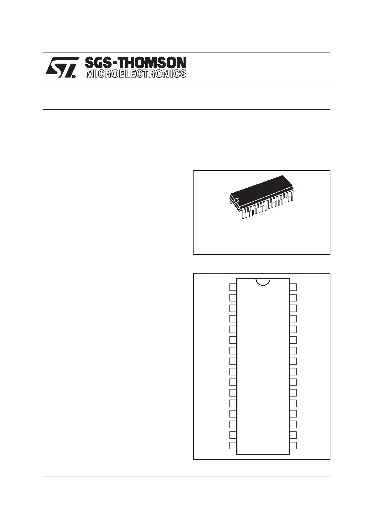
SHRINK32
(Plastic Package)
TDA9110
1
2
3
4
5
6
7
8
9
10
11
12
13
14
15
16
32
31
30
29
28
27
26
25
24
23
22
21
20
19
18
17
5V
SDA
SCL
V
CC
HSIZE
GND
HOUT
XRAY
EWOUT
VOUT
VCAP
V
REF
VAGCCAP
VGND
DCBREATH
GND
9110-01.EPS
December 1997
This isadvance information on a new product now in development or undergoingevaluation. Detailsare subject to change without notice.
1/29
TDA9110
PIN CONNECTIONS
Pin Name Function
1 H/HVIN TTL compatible Horizontal Synchro Input
2 VSYNCIN TTL compatible Vertical Synchro Input (for separated H&V)
3 HMOIRE Horizontal Moire Output (to be connected to PLL2C through a resistordivider)
4 HLOCKOUT First PLL Lock/Unlock Output (0V unlocked -5V locked)
5 PLL2C Second PLL Loop Filter
6 FC1 High Threshold VCO Decoupling Filter
7 C0 Horizontal Oscillator Capacitor
8 R0 Horizontal Oscillator Resistor
9 PLL1F First PLL Loop Filter
10 HPOS Horizontal Position Decoupling Filter
11 HGND Horizontal Section Ground
12 HFLY Horizontal Flyback Input (positive polarity)
13 HREF Horizontal Section Reference Voltage (to be filtered)
14 HLOCKCAP First PLL Lock/Unlock Time Constant Capacitor
15 FOCUSOUT Mixed Horizontal and VerticalDynamic Focus Output
16 HFOCUSCAP Horizontal Dynamic Focus Oscillator Capacitor
17 GND Ground (related internal reference)
18 BREATH DC Breathing Input Control
19 VGND Vertical Section Ground
20 VAGCCAP Memory Capacitor for Automatic Gain Control Loop in Vertical Ramp Generator
21 V
REF
22 VCAP Vertical Sawtooth Generator Capacitor
23 VOUT Vertical Ramp Output (with frequency independantamplitude andSorC Corrections if any).
24 EWOUT East/West Pincushion Correction Parabola Output
25 XRAY X-RAY protection input (with internal latch function)
26 HOUT Horizontal Drive Output (int. trans. open collector)
27 GND General Ground (referenced to V
28 HSIZE DC HSize Control Output
29 V
CC
30 SCL I
31 SDA I
32 5V Supply Voltage(5V Typ.)
Vertical Section Reference Voltage (to be filtered)
It is mixed withvertical position reference voltage output andvertical moire.
)
CC
Supply Voltage (12V Typ)
2
C Clock Input
2
C Data Input
9110-01.TBL
2/29

TDA9110
QUICK REFERENCEDATA
Parameter Value Unit
Horizontal Frequency 15 to 150 kHz
Autosynch Frequency (forgiven R0 and C0) 1 to 4.5 F0
± Horizontal Synchro Polarity Input YES
Polarity Detection (on both Horizontal and Vertical Sections) YES
TTL Composite Synchro YES
Lock/Unlock Identification (on both Horizontal 1st PLL and Vertical Section) YES
2
C Control for H-Position ± 10 %
I
XRay Protection YES
2
C Horizontal Duty Adjust 30 to 60 %
I
2
C Free Running Adjustment NO
I
Stand-by Function YES
Two Polarities H-Drive Outputs NO
Supply Voltage Monitoring YES
PLL1 Inhibition Possibility NO
Horizontal Blanking Output YES
Vertical Frequency 35 to 200 Hz
Vertical Autosync (for 150nF) 50 to 150 Hz
Vertical S-Correction YES
Vertical C-Correction YES
Vertical Amplitude Adjustment YES
DC Breathing Control on Vertical Amplitude YES
Vertical Position Adjustment YES
East/West Parabola Output YES
Pin Cushion Correction Amplitude Adjustment YES
Keystone Adjustment YES
Internal Dynamic HorizontalPhase Control YES
Side Pin Balance Amplitude Adjustment YES
Parallelogram Adjustment YES
Tracking of Geometric Corrections YES
Reference Voltage (both on Horizontal and Vertical) YES
Dynamic Focus (both Horizontal and Vertical) YES
2
C Horizontal Dynamic Focus Amplitude Adjustment YES
I
2
C Horizontal Dynamic Focus Keystone Adjustment YES
I
2
C Vertical Dynamic Focus Amplitude Adjustment YES
I
Type of Input Synchro Detection (suppliedby 5VDigital Supply) YES
Vertical Moiré Output YES
2
C Controlled V-Moiré Amplitude YES
I
Frequency Generator for Burn-in NO
2
C Read/Write 400 kHz
Fast I
Horizontal Moiré Output YES
2
C controlled H-Moiré Amplitude YES
I
DC HSize OutputAmplitude Control YES
9110-02.TBL
3/29
TDA9110
BLOCKDIAGRAM
HOUT
HOUT
BUFFER
CC
V
XRAY
HFOCUSCAP
16
2
X
15 HVFOCUS
CC
17 GND
XRAY
25
V
29
TDA9110
PLL2C
HFLY
FC1
C0
R0
HLOCKCAP
HLOCKOUT
HPOS
PLL1F
5127
6
8914 26
4
10
(5 bits)
H-DUTY
SAFETY
PROCESSOR
PHASE
SHIFTER
2
X
PHASE
COMPARATOR
VCO
LOCK/UNLOCK
IDENTIFICATION
COMPARATOR
H-PHASE (7 bits)
PHASE/FREQUENCY
SYNC
2
X
6 bits
Spin Bal
PROCESSOR
Amp (7bits)
Kest (5 bits)
Key Bal
6 bits
2
X
6 bits
VFOCUS
PCC
7 bits
TRACKING
GEOMETRY
VAMP
7 bits
VPOS
5 bits
VMOIRE
6 bits 6 bits
2
X
7 bits
X
6 bits
Keyst.
VERTICAL
OSCILLATOR
RAMP GENERATOR
S AND C
CORRECTION
20
24
18
22 23
OUT
CAP
V
AGCCAP
V
V
EWOUT
DCBREATH
4/29
REF
V
13
HREF
11
HGND
REF
V
21
VREF
19
VGND
SELECT
SYNC INPUT
1
H/HVIN
(1 bit)
2
VSYNCIN
5 bits
HFLY
VSYNC
3
HMOIRE
28 7 bitsHSIZE
RESET
GENERATOR
31
32
5V
SDA
C INTERFACE
2
I
30
27
SCL
GND
9110-02.EPS
TDA9110
ABSOLUTE MAXIMUMRATINGS
Symbol Parameter Value Unit
V
CC
V
DD
V
IN
VESD ESD susceptibility Human Body Model,100pFDischarge through 1.5kΩ
HSize Cur Max. Sourced Current (Pin 28)
T
stg
T
T
oper
THERMAL DATA
Symbol Parameter Value Unit
R
th (j-a)
SYNCHROPROCESSOR
OperatingConditions
Symbol Parameter Test Conditions Min. Typ. Max. Unit
HsVR Horizontal Synchro Input Voltage Pin 1 0 5 V
MinD Minimum Horizontal Input Pulses Duration Pin 1 0.7 µs
Mduty Maximum Horizontal Input Signal Duty Cycle Pin 1 25 %
VsVR Vertical Synchro Input Voltage Pin 2 0 5 V
VSW Minimum Vertical Synchro Pulse Width Pin 2 5 µs
VSmD Maximum Vertical Synchro Input Duty Cycle Pin 2 15 %
VextM Maximum Vertical Synchro Width on TTL H/Vcomposite Pin 1 750 µs
Supply Voltage (Pin 29) 13.5 V
Supply Voltage (Pin 32) 5.7 V
Max Voltage on Pin12
Pin5
Pin16
Pin7
Pins8, 9, 14, 20,22
Pin15, 18, 23, 24, 25, 26, 28
Pins1, 2, 3, 4, 30, 31
EIAJ Norm,200pF Dischargethrough 0Ω
Max. Sunk Current (Pin 28)
Storage Temperature -40, +150
Junction Temperature +150
j
Operating Temperature 0, +70
Junction-ambient Thermal Resistance Max. 65
(V
DD
=5V,T
amb
=25oC)
1.8
4.0
5.5
6.4
8.0
V
CC
V
DD
2
300
2.5
100
kV
mA
µA
o
o
o
o
C/W
V
V
V
V
V
V
V
V
C
C
C
9110-03.TBL
9110-04.TBL
ElectricalCharacteristics
(V
DD
=5V,T
amb
=25oC)
Symbol Parameter Test Conditions Min. Typ. Max. Unit
VINTH Horizontaland Vertical Input Threshold Voltage
(Pins 1, 2)
Low Level
High Level 2.2
0.8 V
RIN Horizontaland Vertical Pull-Up Resistor Pins 1, 2 200 kΩ
VOut Output Voltage (Pin 4) Low level
High Level
0
5
TfrOut Falling and Rising Output CMOS Buffer Pin 4, Cout = 20pF 200 ns
VHlock Horizontal 1st PLL Lock Output Status (Pin 4) Locked
Unlocked
VoutT Extracted Vsync Integration Time (% of T
Composite
) on H/V
H
C0 = 820pF 26 35 %
0
5
I2C READ/WRITE
ElectricalCharacteristics
Symbol Parameter Test Conditions Min. Typ. Max. Unit
2
C PROCESSOR
I
Fscl Maximum Clock Frequency Pin 30 400 kHz
Tlow Low period of the SCL Clock Pin 30 1.3 µs
Thigh Highperiod of the SCL Clock Pin 30 0.6 µs
Vinth SDA and SCL Input Threshold Pins 30,31 2.2 V
VACK Acknowledge Output Voltage onSDA input with 3mA Pin31 0.4 V
See also I2CTable Control and I2C Sub Address Control
(V
DD
=5V,T
amb
=25oC)
V
V
V
V
V
9110-05.TBL
5/29
TDA9110
HORIZONTALSECTION
OperatingConditions
Symbol Parameter Test Conditions Min. Typ. Max. Unit
VCO
R
0(Min.)
C
0(Min.)
F
(Max.)
OUTPUT SECTION
I12m Maximum Input Peak Current Pin 12 2 mA
HOI Horizontal Drive Output Maximum Current Pin 26, Sunk
Minimum Oscillator Resistor Pin 8 4 kΩ
Minimum Oscillator Capacitor Pin 7 390 pF
Maximum Oscillator Frequency 150 kHz
30 mA
current
ElectricalCharacteristics
(V
CC
=12V,T
amb
=25oC)
Symbol Parameter Test Conditions Min. Typ. Max. Unit
SUPPLY AND REFERENCE VOLTAGES
V
V
I
I
V
REF-H
V
REF-V
I
REF-H
I
REF-V
Supply Voltage Pin 29 10.8 12 13.2 V
CC
Supply Voltage Pin 32 4.5 5 5.5 V
DD
Supply Current Pin 29 50 mA
CC
Supply Current Pin 32 5 mA
DD
Horizontal Reference Voltage Pin13, I = 5mA 7.4 8 8.6 V
Vertical Reference Voltage Pin 21, I = 5mA 7.4 8 8.6 V
Max. SourcedCurrent on V
Max. SourcedCurrent on V
REF-H
REF-V
Pin 13 5 mA
Pin 21 5 mA
1st PLL SECTION
HpolT Polarity Integration Delay 0.75 ms
V
VCO ControlVoltage (Pin9) V
VCO
Vcog VCO Gain (Pin 9) R
=8V
REF-H
f
0
fH(Max.)
= 5.9kΩ,C0= 820pF,
0
dF/dV = 1/11R
0C0
V
/6
REF-H
6.2
18.8 kHz
Hph HorizontalPhase Adjustment % of Horizontal Period ±10 %
Hphmin
Hphtyp
Hphmax
f
0
Minimum Value
Typical Value
Maximum Value
Free Running Frequency R0= 5.9kΩ,C0= 820pF,
dF0/dT FreeRunning FrequencyThermal Drift
Horizontal Phase Setting Value
Sub-Address 01
Byte x1111111
Byte x1000000
Byte x0000000
2.6
3.2
3.8
25 kHz
= 0.97/8R0C
f
0
0
See Note -150 ppm/C
(No drift on external components)
CR PLL1 Capture Range R
Note : This parameter is not tested on eachunit. It is measured during our internalqualification.
= 6.49kΩ,C0= 820pF,
0
+0.5kHz to 4.5F
from f
0
fH(Min.)
(Max.)
f
H
Component accuracy :
= 2%, R0=1%
C
0
0
28 kHz
100
V
V
V
V
V
kHz
9110-05.TBL
6/29

TDA9110
HORIZONTALSECTION (continued)
ElectricalCharacteristics
Symbol Parameter Test Conditions Min. Typ. Max. Unit
2nd PLL SECTION AND HORIZONTAL OUTPUT SECTION
FBth Flyback Input Threshold Voltage (Pin12) 0.65 0.75 V
Hjit Horizontal Jitter Horizontal Freq. = 31kHz 60 ppm
Horizontal Drive Output Duty-Cycle
HDmin
HDmax
XRAYth X-RAY Protection Input Threshold Voltage Pin 25 8 V
Vphi2 Internal Clamping Levels on 2nd PLL Loop
VSCinh Threshold Voltage To Stop H-Out,V-Out
HDvd Horizontal Drive Output (low level) Pin 26I
HORIZONTAL DYNAMIC FOCUS FUNCTION
HDFst Horizontal Dynamic Focus Sawtooth
HDFdis Horizontal Dynamic Focus Sawtooth
HDFstart Internal fixed Phase Advance versus Hfly
HDFDC Bottom DC Output Level R
TDHDF DC Output Voltage Thermal Drift 200 ppm/C
HDFamp Horizontal Dynamic Focus Amplitude
HDFKeyst Horizontal Dynamic Focus Keystone
VERTICAL DYNAMIC FOCUS FUNCTION (positive parabola)
AMPVDF Vertical Dynamic FocusParabola (added
VDFAMP Parabola Amplitude Function of VAMP
VHDFKeyt Parabola Assymetry Function of VPOS
Notes :
(Pin 26) (see Notes 1 & 2)
Low Level
High Level
Filter (Pin5)
when V
< VSCinh
CC
Minimum Level
Maximum Level
Discharge Width
Middle
Min Byte x1111111
Typ Byte x1000000
Max Byte x0000000
Min A/B Byte xxx11111
Typ Byte xxx10000
Max A/B Byte xxx00000
to horizontal one) Amplitude with VOUT
and VPOS Typical
Min. Byte 000000
Typ. Byte 100000
Max. Byte 111111
(tracking between VAMP and VDF) with
VPOS Typ.
(see Figure 1 and Note 3)
Control (tracking between VPOS and VDF)
with VAMP Max.
1. DutyCycle is theratio of power transistor OFF time period. Power transistor is OFF when output transistor is OFF.
2. Initial Conditionfor Safe Operation Start Up
3. S and C correction are inhibitedso the output sawtooth has a linear shape.
(V
CC
=12V,T
=25oC) (continued)
amb
Sub-Address 00
Byte xxx11111
Byte xxx00000
Low Level
High Level
Pin 29 7.5 V
HfocusCap = C
TH=TBD, Pin 16 2
Start by HDFstart 400 ns
Fixed for each frequency
(Pin 16)
LOAD
Sub-Address 03, Pin 15,
FH = 50kHz, Keystone Typ 1.1
Sub-Address 04,
FH = 50kHz, TypAmp
B/A
A/B
A/B
Sub-Address 0F
Sub-Address 05
Byte 10000000
Byte 11000000
Byte 11111111
Sub-Address 06
Byte x0000000
Byte x1111111
30
60
1.6
3.7
= 30mA 0.4 V
OUT
= 820pF,
0
4.7
860 ns
= 10kΩ, Pin 15 2 V
1.7
3.5
2.5
1.0
2.5
0
0.5
1
0.6
1
1.5
0.52
0.52
%
%
V
V
V
V
V
PP
V
PP
V
PP
V
PP
V
PP
V
PP
V
PP
V
PP
V
PP
9110-05.TBL
7/29
TDA9110
VERTICALSECTION
OperatingConditions
Symbol Parameter Test Conditions Min. Typ. Max. Unit
OUTPUTS SECTION
VEWM Maximum EW Output Voltage Pin24 6.5 V
VEWm MinimumEW Output Voltage Pin24 1.8 V
R
LOAD
Minimum Load for less than 1% Vertical Amplitude Drift Pin 20 65 MΩ
ElectricalCharacteristics
(V
CC
=12V,T
amb
=25oC)
Symbol Parameter Test Conditions Min. Typ. Max. Unit
VERTICAL RAMP SECTION
VRB Voltage at Ramp Bottom Point V
VRT Voltage at Ramp TopPoint(withSynchro)V
REF-V
VRTF Voltage at Ramp Top Point (without Synchro) Pin 22 VRT-
=8V, Pin 22 2 V
REF-V
Pin 22 5 V
V
0.1
VSTD Vertical Sawtooth Discharge Time Duration (Pin
With 150nF Cap 70 µs
22)
VFRF Vertical FreeRunning Frequency
(see Notes 4 & 5)
ASFR AUTO-SYNC Frequency C
RAFD Ramp Amplitude Drift versus Frequency at
Maximum Vertical Amplitude
Rlin Ramp Linearity on Pin 22 (seeNotes 4 & 5) 2.5 < V
Vpos Vertical Position Adjustment Voltage
(Pin23 - VOUT centering)
VOR Vertical Output Voltage
(peak-to-peak on Pin 23)
C
OSC (Pin22)
Measured on Pin22
22
See Note 6
C
22
50Hz < f and f < 165Hz
= 150nF
= 150nF ±5%
= 150nF
and V22<4.5V 0.5 %
22
Sub Address 06
Byte x0000000
Byte x1000000
Byte x1111111 3.65
Sub Address 05
Byte x0000000
Byte x1000000
Byte x1111111 3.5
100 Hz
50 165 Hz
200 ppm/Hz
3.2
3.3 V
3.5
3.8
2.25
2.5 V
3
3.75
V
V
V
V
VOI Vertical Output Maximum Current (Pin23) ±5mA
dVS Max Vertical S-Correction Amplitude
x0xxxxxx inhibits S-CORR
x1111111 gives max S-CORR
Ccorr Vertical C-Corr Amplitude
x0xxxxxx inhibits C-CORR
Notes : 4. With Register07 at Byte x0xxxxxx (VerticalS-Correction Control) then the S correction is inhibited, consequentlythe sawtooth has
a linear shape.
5. WithRegister 08 at Byte x0xxxxxx (VerticalC - Correction Control) then the C correction is inhibited, consequently the sawtooth
has a linear shape.
6. It is the frequency range for which the VERTICAL OSCILLATOR will automaticallysynchronize, using a single capacitor value on
Pin 22 and with a constant ramp amplitude.
Subaddress 07
PP
PP
at T/4
at 3T/4
∆V/V
∆V/V
SubAddress 08
Byte x1000000
Byte x1100000
Byte x1111111
-4
+4
-3
%
%
%
0
3
%
%
9110-05.TBL
8/29

VERTICALSECTION(continued)
ElectricalCharacteristics
Symbol Parameter Test Conditions Min. Typ. Max. Unit
EAST/WEST FUNCTION
EW
DC
TDEW
EWpara Parabola Amplitude with Vamp Max,
EWtrack ParabolaAmplitude Function of V-AMP Control
KeyAdj KeystoneAdjustment Capabilitywith Typ Vpos,
KeyTrack Intrinsic Keystone Function of V-POS Control
DC HSIZE OUTPUTCONTROL
HSize out DC HSize Output Level (Pin28) Subaddress 0B
INTERNAL HORIZONTAL DYNAMIC PHASE CONTROL FUNCTION
SPBpara SidePin Balance ParabolaAmplitude(Figure 3)
SPBtrack Side Pin Balance Parabola Amplitude function
ParAdj ParallelogramAdjustmentCapability with Vamp
Partrack IntrinsicParallelogram FunctionofVposControl
VERTICAL MOIRE
VMOIRE Vertical Moire (measuredon VOUTDC) (Pin23) Subaddress 0C
BREATHING COMPENSATION
BRADj Vertical Output Variation versus DC Breathing
Notes :
7. These parameters are not tested on each unit. They are measured during our internalqualification
8. Refersto Notes 4 & 5 from last section.
9. TH is the Horizontal PLL Period Duration.
DC Output Voltage with Typ Vpos,Keystone,
Corner and Corner Balance Inhibited
DC Output Voltage Thermal Drift See Note 7 100 ppm/C
DC
V-Pos Typ, Keystone Inhibited
(tracking between V-AMP and E/W) with Typ
Vpos, Keystone, EW Typ Amplitude
(see Note 8)
EW Inhibited and Vertical Amplitude Max.
(see Note 8 and Figure 4)
(tracking between V-POS and EW) with EW
Max Amplitude and Vertical Amplitude Max.
(see Note 8)
A/B Ratio
B/A Ratio
with Vamp Max, V-POS Typand Parallelogram
Inhibited (see Notes 8 & 9)
of Vamp Control (tracking between Vamp and
SPB) w ith SPB Max, V-POS Typ and
Parallelogram Inhibited (see Notes 8 & 9)
Max, V-POS Typ and SPB Max
(see Notes 8 & 9)
(trackingbetween V-Pos andDHPC)withVamp
Max, SPB Max and Parallelogram Inhibited
(see Notes 8 & 9)
A/B Ratio
B/A Ratio
Control (Pin 23)
(V
CC
=12V,T
=25oC) (continued)
amb
Pin 24, see Figure 2 2.5 V
Subaddress 0A
Byte 11111111
Byte 10100000
Byte 10000000
2.5
1.25
0
Subaddress 05
Byte 10000000
Byte 11000000
Byte 11111111
0.45
0.8
1.25
Subaddress 09
Byte 1x000000
Byte 1x111111
0.9
0.9
Subaddress 06
Byte x0000000
Byte x1111111
Byte 00000000
Byte 01000000
Byte 01111111
0.52
0.52
0.5
2.5
4.5
Subaddress 0D
Byte x1111111
Byte x1000000
+1.4
-1.4
Subaddress 05
Byte 10000000
Byte 11000000
Byte 11111111
0.5
0.9
1.4
Subaddress 0E
Byte x1111111
Byte x1000000
+1.4
-1.4
Subaddress 06
Byte x0000000
Byte x1111111
0.52
0.52
Byte 01x11111 6 mV
V
18>VREF-V
V18=V
V18=V
REF-V
REF-V
-4V
0
0
-10
TDA9110
V
V
V
V
V
V
V
PP
V
PP
V
V
V
%TH
%TH
%TH
%TH
%TH
%TH
%TH
%
%
%
9110-05.TBL
9/29

TDA9110
Figure1 : VerticalDynamic Focus Function
VDF
VDF
DC
AMP
A
Figure3 :
DynamicHorizontal Phase Control
Output
B
A
SPB
PARA
DHPC
Figure2 : E/W Output
EW
B
9110-03.EPS
A
Figure4 :
EW
DC
KeystoneEffect on E/WOutput
PARA
B
9110-04.EPS
(PCC Inhibited)
Keyadj
DC
9110-05.EPS
9110-06.EPS
10/29

TYPICALVERTICAL OUTPUT WAVEFORMS
Function
Vertical Size 05 23
Sub
Address
Pin Byte Specification Picture Image
10000000
11111111
V
V
OUTDC
OUTDC
TDA9110
2.25V
3.75V
Vertical
Position
DC
Control
Vertical
S
Linearity
Vertical
C
Linearity
06 23
07 23
08 23
x0000000
x1000000
x1111111
0xxxxxxx
Inhibited
1x111111
1x000000
1x111111
3.2V
3.5V
3.8V
∆V
V
PP
∆V
=4%
V
PP
V
PP
V
PP
∆V
∆V
∆V
=3%
V
PP
∆V
=3%
V
PP
9110-06.TBL/ 9110-07.EPS TO 9110-13.EPS
11/29

TDA9110
GEOMETRY OUTPUT WAVEFORMS
Function
Sub
Address
Pin Byte Specification Picture Image
EWamp
Inhibited.
1X000000
0.9V
2.5V
Trapezoid
Control
Pin Cushion
Control
Parrallelogram
Control
Side Pin
Balance
Control
09 24
0A 24
0E Internal
0D Internal
1X111111
Keystone
Inhibited
10000000
11111111
SPB
Inhibited
1x000000
1x111111
Parallelogram
Inhibited
1x000000
1x111111
0.9V
2.5V
3.7V
3.7V
3.7V
3.7V
2.5V
0V
2.5V
1.4% TH
1.4% TH
1.4% TH
1.4% TH
Vertical
Dynamic
Focus
with Horizontal
12/29
32
2V
9110-07.TBL/ 9110-14.EPS TO 9110-22.EPS

TDA9110
I2C BUSADDRESS TABLE
SubAddress Definition
Slave Address (8C) : Write Mode
D8 D7 D6 D5 D4 D3 D2 D1
0 x x x x 0 0 0 0 Horizontal Drive Selection / Horizontal Duty Cycle
1 x x x x 0 0 0 1 Horizontal Position
2 x x x x 0 0 1 0 Horizontal Moiré Control
3 x x x x 0 0 1 1 Synchro Priority / Horizontal Focus Amplitude
4 x x x x 0 1 0 0 Refresh / Horizontal Focus Keystone
5 x x x x 0 1 0 1 Vertical Ramp Amplitude
6 x x x x 0 1 1 0 Vertical Position Adjustment
7 x x x x 0 1 1 1 S Correction
8 x x x x 1 0 0 0 C Correction
9 x x x x 1 0 0 1 E/W Keystone
A x x x x 1 0 1 0 E/W Amplitude
B x x x x 1 0 1 1 Horizontal Size Control
C x x x x 1 1 0 0 Vertical Moiré
D x x x x 1 1 0 1 Side Pin Balance
E x x x x 1 1 1 0 Parallelogram
F x x x x 1 1 1 1 Vertical Dynamic Focus Amplitude
Slave Address (8D) :
D8 D7 D6 D5 D4 D3 D2 D1
0 x x x x 0 0 0 0 Synchro and Polarity Detection
ReadMode
13/29

TDA9110
2
C BUSADDRESS TABLE (continued)
I
D8 D7 D6 D5 D4 D3 D2 D1
WRITE MODE
00
01
02
03
04
05
06
07
08
09
0A
0B
0C
0D
0E
0F
READ MODE
00
[] initial value
Xray
1, reset
[0]
HMoire
1, on
[0], off
Sync
0, Comp
[1], Sep
Detect
Refresh
[0], off
Vramp
0, off
[1], on
S Select
1, on
[0]
C Select
1, on
[0]
EW Key
0, off
[1]
EW Sel
0, off
[1]
Test H
1, on
[0], off
Test V
1, on
[0], off
SPB Sel
0, off
[1]
Parallelo
0, off
[1]
Hlock
0, on
[1], no
HDrive
0, off
[1], on
[1] [0] [0] [0] [0] [0] [0]
[1] [0] [0] [0] [0] [0] [0]
[1] [0] [0] [0] [0] [0] [0]
[1] [0] [0] [0] [0] [0] [0]
[1] [0] [0] [0] [0] [0]
[1] [0] [0] [0] [0] [0]
[1] [0] [0] [0] [0] [0]
[1] [0] [0] [0] [0] [0] [0]
[1]
Moire
1, on
[0]
Vlock
0, on
[1], no
[0] [0] [0] [0] [0] [0]
[1] [0] [0] [0] [0] [0]
[1] [0] [0] [0] [0] [0]
[1] [0] [0] [0] [0] [0]
Xray
1, on
[0], off
Horizontal Duty Cycle
[0] [0] [0] [0] [0]
Horizontal Phase Adjustment
Horizontal Moire Amplitude
[0] [0] [0] [0] [0]
Horizontal Focus Amplitude
Horizontal Focus Keystone
[1] [0] [0] [0] [0]
Vertical Ramp Amplitude Adjustment
Vertical Position Adjustment
S Correction
C Correction
East/West Keystone
East/West Amplitude
HSize Control
Vertical Moire
[0] [0] [0] [0] [0]
Side Pin Balance
Parallelogram
Vertical Dynamic FocusAmplitude
Polarity Detection Synchro Detection
H/V pol
[1], negative
V pol
[1], negative
Vext det
[0], no det
H/V det
[0], no det
V det
[0], no det
Dataare transferredwith vertical sawtooth retrace.
14/29

OPERATINGDESCRIPTION
I - GENERAL CONSIDERATIONS
I.1 - Power Supply
The typical values of the power supply voltages
V
and VDDare12Vand 5V respectively. Perfect
CC
operation is obtained for V
13.2Vand V
between4.5 and 5.5V.
DD
between 10.8 and
CC
In order to avoid erratic operation of the circuit
during transient phase of V
the value of V
is monitored and the outputs of
CC
the circuit are inhibited if V
switchingon, or off,
CC
is less than 7.5V
CC
typically.
Similarly,V
until V
DD
is monitored and internally set-up
DD
reaches 4V (see I2C Control Table for
poweron reset).
Inordertohaveaverygoodpowersupplyrejection,
the circuit is internallysuppliedby severalvoltage
references(typicalvalue:8V).Twoofthesevoltage
references are externally accessible, one for the
vertical and one forthe horizontalpart. If needed,
these voltage references can be used (if I
LOAD
less than 5mA). It is necessary to filter the a.m.
voltage references by external capacitors connected to ground, in order to minimize the noise
and consequently the ”jitter” on vertical and horizontaloutput signals.
2
C Control
I.2 - I
TDA9110belongsto the I
2
Ccontrolleddevice family. Insteadof being controlled by DC voltages on
dedicated control pins, each adjustment can be
donevia the I
2
C bus is a serial buswith a clockand a data
TheI
2
C Interface.
input.Thegeneralfunctionandthebusprotocolare
specifiedin the Philips-bus data sheets.
The interface (Data and Clock) is TTL-level compatible. The internal threshold level of the input
comparatoris 2.2V (when V
is 5V). Spikes (up
DD
to 50ns) are filtered by an integratorand the clock
speedis limited to 400kHz.
Thedataline(SDA)canbeusedbidirectionally(i.e.
in read-mode the IC clocks out a reply information
(1 byte) to themicro-processor).
The bus protocol prescribes always a full-byte
transmission.Thefirst byte after the start condition
is used to transmit theIC-address(7 bits-8C) and
the read/writebit (0write - 1 read).
I.3 - Write Mode
In write mode the second byte sent contains the
subaddress of the selected function to adjust (or
controlsto affect)andthe thirdbytethecorresponding data byte.Itis possibleto send more than one
databyteto the IC.If afterthe thirdbyteno stop or
start condition is detected, the circuit increments
automaticallyby onethemomentarysubaddressin
the subaddress counter (auto-increment mode).
So it is possible to transmit immediately the next
data bytes without sending the IC address or
subaddress.It canbeusefultoreinitializethewhole
controls very quickly (flash manner). This procedure can be finishedby a stop condition.
Thecircuithas16adjustmentcapabilities: 2forthe
Horizontal part, 4 for the Vertical, 2 for the E/W
correction, 2 for the Dynamic Horizontal phase
control,2for the Moire options,3 for the Horizontal
and Vertical Dynamic Focus and 1 for the HSize
amplitudecontrol.
15 bits are also dedicated to several controls
(ON/OFF, SynchroPriority, Detection Refreshand
Xray reset).
I.4 - Read Mode
During the read mode the second byte transmits
the reply information.
The reply bytecontainsthe Horizontaland Vertical
Lock/Unlockstatus, the Xray activationstatusand,
is
theHorizontaland Verticalpolaritydetection.It also
contains the Synchro detection status which is
used by theMCU to assignthe Synchro priority.
Astopconditionalwaysstopsallthe activitiesof the
bus decoderand switchesto high impedanceboth
for the data and the clock line (SDA and SCL).
2
C Subaddressand controltables.
See I
I.5 - SynchroProcessor
TheinternalSynchroProcessorallowstheTDA9110
toacceptany kind of input synchrosignals:
- separated Horizontal & Vertical TTL-compatible
synchrosignals,
- composite Horizontal &Vertical TTL-compatible
synchrosignals.
I.6 - SynchroIdentificationStatus
The MCU can choose via the I
2
C the synchro
priority thanks to the system identification status
provided by the TDA9110. The extracted Vertical
synchro pulse is available when this identification
status has been received and when the 12V is
supplied.EveninPowermanagementmodethe IC
isabletoinformtheMCUthatsynchrosignalswere
detected due to its 5V supply. We recommend to
use the device as following : first, refresh the synchrodetectionby I
det and Vdet by I
2
C, thencheckthe status of H/V
2
C read.
Sync priority choice should be :
Vext
H/V
det
detVdet
No Yes Yes 1 1 Separated H & V
Yes Yes No 0 1 Composite TTL
Sync priority
Subaddress 03
D8 D7 Synchro type
H&V
TDA9110
Comment
15/29

TDA9110
OPERATINGDESCRIPTION(continued)
Ofcourse,whenthechoiceisdone,wecanrefresh
thesynchrodetectionsandverifythattheextracted
Vsyncis present and thatno synchro typechange
have occured.
Synchro processor is also giving synchro polarity
information.
I.7 - IC status
TheICcaninformthe MCUaboutthe1stHorizontal
PLL or Verticalsection status (locked or not), and
aboutthe Xray protection(activatedor not).
ResettingtheXrayinternallatchcan bedoneeither
by decreasingthe V
via the I
2
C interface.
I.8 - Synchro Inputs
Both H/HVin and Vsyncin inputs are TTL compatible triggers with Hysterisis to avoid erratic detection. It includes pull up resistor to V
I.9 - Synchro ProcessorOutput
ThesynchroprocessordeliverstheHlockoutsignal
on a TTL-compatible CMOS output.
HlockoutistheHorizontal1stPLLstatus(5Vwhen
locked).It allows the MCU tocheck the Horizontal
IC locking.
II - HORIZONTAL PART
II.1 - Internal Input Conditions
A digital signal (Horizontal synchro pulse or TTL
composite)is sentby thesynchro processorto the
horizontalpart.
Positive or negative signal can be applied to the
Horizontalpart input (see Figure 6).
Using internal integration,both signals are recognized if Z/T < 25%. Synchronization occurs on the
leading edge of the internal synchro signal. The
minimumvalue of Z is0.7µs.
supplyor directlyresetting
CC
.
DD
Figure 7
C
TRAMEXT
dd
The last feature performed is the removing of
equalizing pulses to avoid parasitic pulses on
phase comparator input (which is sensitive to
wrongor missingpulses).
II.2 - PLL1
ThePLL1consistsof a phasecomparator,anexternalfilteranda voltagecontrol oscillator(VCO).
Thephase comparatoris a ”phasefrequency”type
designedin CMOS technology. This kind of phase
detector avoids locking on false frequencies. It is
followed by a ”charge pump”, composed of two
currentsourcessunkandsourced(TypicallyI =1mA
when locked and I = 140µA when unlocked). This
difference between lock/unlock permits a smooth
catching of the horizontal frequency by the PLL1.
This effectis reinforced by an internaloriginal slow
downsystemwhenthePLL1is locked,avoidingthe
Horizontalfrequencyto changetoofast.
The dynamic behaviour of thePLL1 is fixedby an
external filter which integrates the current of the
chargepump. A”CRC”filter is generallyused(see
Figure 8).
Figure 8
PLL1F
7
9110-24.EPS
Figure6
Anotherintegrationisable to extractverticalpulse
of composite synchro if duty cycle is higher than
25%(typicallyd =35%) (see Figure 7).
16/29
ThePLL1isinternall yinhibit edduringextractedver ti c al
synchro (if any) to avoid taking in account missing
pulses or wr ong pulses on phase compar ator.The
inhibition resultsfrom theopening of a switc hlocated
betweenthechargepumpandthefilter(seeFigure9).
TheVCO usesan externalRC network. It delivers
9110-23.EPS
a linearsawtooth obtained by the chargeand the
discharge of the capacitor, with a current proportionnal to the current in the resistor. The typical
thresholdsof the sawtoothare 1.6Vand 6.4V.
9110-25.EPS

OPERATINGDESCRIPTION(continued)
Figure9 : Principle Diagram
H-LOCKCAP
TDA9110
8
LOCK/UNLOCK
STATUS
PLL1F R0 C0
765
LOCKDET
HSYNC
INPUT
INTERFACE
TRAMEXT
COMP1
E2
Figure10 : Detailsof VCO
I
0
2
I
0
Loop
7
Filter
4I
(1.3V < V < 6V)
7
6
R0
The control voltageof the VCO is between 1.33V
and 6V (see Figure 10). The theorical frequency
range of this VCO is in the ratio of 1 to 4.5. The
effectivefrequency range has to be smaller (1 to
4.2)duetoclampinterventiononfilterlowestvalue.
Inorder toincrease this effectivefrequencyrange,
toapossiblerangeof1to6.0onecanadda resistor
fromPin 6 to Href leading.
Thesynchrofrequencymustalwaysbe higherthan
the free running frequency. For example, when
usinga synchro range between31kHz and 96kHz,
thesuggestedfree running frequencyis 25kHz.
The PLL1 ensures the coincidence between the
leading edge of the synchro signal and a phase
reference obtained by comparison between the
sawtooth of the VCO and an internal DC voltage
whichis I
2
C adjustablebetween 2.65V and 3.75V
(correspondingto ± 10%)(see Figure 11).
TRAMEXT
High
Low
0
CHARGE
PUMP
6.4V
1.6V
6.4V
10
C0
1.6V
Figure 11 :
0 0.875T
PLL
INHIBITION
I2C
PHASE
ADJUST
T
H
FLIP FLOP
HPOS
Adj.
RS
PLL1TimingDiagram
VCO
H Osc
Sawtooth
7/8T
H
1/8T
H
2.60V<Vb<3.80V
Phase REF1
H Synchro
Phase REF1is obtainedby comparisonbetween thesawtoothand
a DC voltage adjustable between 2.60V and 3.80V. The PLL1
ensures the exact coincidence between the signals phase REF
and HSYNS. A ± T/10 phase adjustment is possible.
OSC
9110-26.EPS
9110-27.EPS
6.4V
Vb
1.6V
9110-28.EPS
17/29

TDA9110
OPERATINGDESCRIPTION(continued)
Figure12 : LOCK/UNLOCKBlock Diagram
From
Phase
Comparator
NOR1
A
TheTDA9110also includes a Lock/Unlockidentificationblockwhich senses in realtime whetherthe
thePLL1is lockedornotontheincominghorizontal
synchro signal. The resulting information is available on Hlockout (see Synchro Processor). The
blockfunction is described in Figure 12.
The NOR1 gate receive the phase comparator
output pulses (whichalso drive the charge pump).
Whenthe PLL1islocked,wehaveonpointAavery
small negative pulse (about 100ns) at each horizontal cycle, so after the RC filter, there is a high
levelon Pin 14 whichforcesHlockouttohigh level.
The hysterisis comparator detects locking when
Pin 14 reachs 6.5V and unlocking when Pin 14
decreasesto 6.0V.
When the PLL1 is unlocked, the 100ns negative
pulseon Abecomesmuchlargerandconsequently
the average level on Pin 14 decreases. It forces
Hlockoutto low level.
ThePin 14 status is approximatelythe following:
- near0V when there is no H-Sync
- between0 and 4V withH-Sync frequencydifferent from VCO
- between4 to 8 V when VCO frequencyreaches
H-Sync one (but not already in phase)
- near8V when PLL1 is locked.
It is important to notice that Pin 14 is not an
output pin but is only used for filtering purpose
(see Figure 12).
The lock/unlock information is also available
throughthe I
2
C read.
II.3 - PLL2
The PLL2 ensures a constant position of the
shapedflybacksignal in comparisonwith the sawtoothof the VCO (Figure13).
The phase comparator of PLL2 (phase type comparator) is followed by a charge pump (typical
output current: 0.5mA).
The flyback input consists of an NPN transistor.
This input must be current driven. The maximum
20kΩ
220nF
5V
H-Lock CAP
6V
B
3 HLOCKOUT
8
6.5V
recommanded input current is 5mA (see Figure 14).
Theduty cycle is adjustablethrough I
2
to60%. For Start Up safe operation, the initial duty
cycle(afterPoweronreset)is 60% inordertoavoid
to have a toolong conductionof theBU transistor.
Themaximumstoragetimeisabout38%(T
Typically,T
isaround20%whichmeansthat
FLY/TH
Tsmax is around28%.
Figure 13 :
Flyback
Internally
Shaped
H Drive
The duty cycle of H-drive is adjustable between 30% and 60%.
PLL2TimingDiagram
H Osc
Sawtooth
Flyback
7/8T
Ts
Duty Cycle
H
1/8T
H
Figure 14 : Flyback Input Electrical Diagram
400Ω
HFLY
12
20kΩ
GND 0V
Q1
C from30%
/2.TH).
FLY
6.4V
3.7V
1.6V
9110-29.EPS
9110-30.EPS
9110-31.EPS
18/29

OPERATINGDESCRIPTION(continued)
II.4 - Output Section
The H-drive signal is sent to theoutput through a
shaping block ensuring Ts and H-drive duty cycle
(I2Cadjustable)(seeFigure13).In orderto secure
the scanning power part operation, the output is
inhibitedin the followingcases :
- whenV
is too low,
CC
- whenthe Xray protectionis activated,
- duringthe Horizontal flyback,
- whenthe HDrive I
2
C bit controlis off.
Theoutputstageconsistsofa NPNbipolartransistor.Onlythe collectoris accessible(seeFigure15).
Figure15
V
CC
H-DRIVE26
The output NPN is in off-state when the power
scanningtransistoris alsoin off-state.
The maximum output current is 30mA, and the
correspondingvoltagedrop of theoutput V
CEsat
0.4V typically.
Obviouslythe powerscanningtransistorcannotbe
directlydrivenby theintegratedcircuit.Aninterface
hasto beaddedbetweenthe circuitand the power
transistoreitherof bipolar or of MOS type.
II.5 - X-RAYProtection
TheX-Ray protection is activatedby applicationof
a highlevel on theX-Rayinput (8Von Pin25).The
consequenciesof X-Ray protectionare :
- inhibitionof H-Driveoutput
- activationof vertical blankingoutput.
This protection is reseteither by V
2
C (see Figure 16).
by I
CC
II.6 - Horizontal and VerticalDynamic Focus
TheTDA9110 deliversa horizontalparabolawhich
is added on a vertical parabola waveform on Pin
15. This horizontal parabola comes from a sawtooth. The phase advance versus Horizontal flyback middle is kept constant for each frequency
(about 860ns). This sawtooth is present on Pin 16
where the horizontal focus capacitor is the same
as C0 to obtain a controlled amplitude (from 2 to
4.7Vtypically).
9110-32.EPS
Symmetry(keystone)andamplitudeareI
able(seeFigure 17).The Verticaldynamicfocusis
trackedwithVPOSand VAMP.Itsamplitudecanbe
adjusted.It is also affectedby S andC corrections.
Thispositivesignal has tobeconnectedtotheCRT
is
focusinggrids.
TDA9110
switch off or
2
Cadjust-
Figure16 : SafetyFunctions Block Diagram
V
Checking
CC
V
CC
Ref
XRAYProtection
XRAY
VCCoff or I2C Reset
Horizontal Flyback
0.7V
S
Q
R
2
C Drive on/off
I
2
I
C Ramp on/off
HORIZONTAL
OUTPUT
INHIBITION
VERTICAL
OUTPUT
INHIBITION
9110-33.EPS
19/29

TDA9110
OPERATINGDESCRIPTION(continued)
Figure17
Horizontal Flyback
Internal Trigged
Horizontal Flyback
Horizontal Focus
Cap Sawtooth
Horizontal Dynamic
Focus Parabola
Output
II.7 - Moire Output
The moire output is intented to correct a beat
betweenthe horizontalvideo pixel period and the
currentCRT pixel width.
Themoiresignalisa combinationof theHorizontal
and the Verticalfrequencysignals.
To achieve a moire cancellation, the moire output
has to be connected to any point of the chassis
controllingthe horizontalposition.We recommend
to introduce this “ Horizontal Controlled Jitter” on
MoireOutput
860ns
4.7V
400ns
2V
2V
the relative ground of PLL2 capacitor where this
“controlled jitter” frequency type will directly affect
the horizontalposition.
2
The amplitude of the signal is I
C adjustable.
If theH-Moirefeature is not necessaryin theapplication, the H-Moire output (Pin3) can be usedas
a 5bits DAC output(0.3V to 2.2V). If the H-Moire
outputisnotusedat all,so the Pin3 must beeither
kept to highimpedanceor grounded via a resistor.
9110-34.EPS
20/29

OPERATINGDESCRIPTION(continued)
III - VERTICAL PART
III.1- Geometric Corrections
Theprinciple is representedon Figure20.
Startingfrom the verticalramp, a parabolashaped
current is generated for E/W correction, dynamic
horizontal phase control correction, and vertical
dynamicFocus correction.
The parabola generator is made by an analog
multiplier, the output current of which is equal to :
∆
I=k⋅(V
OUT-VDCOUT
2
)
where Vout is the vertical output ramp (typically
between 2 and 5V) and Vdcout is the vertical DC
output adjustablein the range 3.2V to 3.8V which
generate a dissymetric parabola if needed (keystoneadjustment).
In order to keep a good screen geometry for any
enduserpreferencesadjustment,weimplemented
the ”geometry tracking”.
Due to large output stages voltage range (E/W,
FOCUS),thecombinationof trackingfunctionwith
maximum vertical amplitude max or min vertical
position and maximum gain on the DAC control
mayleadto the outputstagessaturation.This must
Figure20 :
GeometricCorrections Principle
TDA9110
be avoided by limiting the output voltage with apropriateI
FortheE/Wpartandthe DynamicHorizontalphase
controlpart, a sawtoothshaped differentialcurrent
in the followingform is generated:
Then ∆I and ∆I’ are addedandconverted into voltage for the E/W part.
Each of the two E/W components or the two DynamicHorizontalphasecontrolonesmaybeinhibited by theirown I
The E/W parabola is available on Pin 24 via an
emitter follower which has to be biased by an
externalresistor(10kΩ). It canbe DCcoupled with
externalcircuitry.
The VerticalDynamic Focus is combinedwith the
Horizontalone on Pin15.
ThedynamicHorizontalphasecontrolcurrentdrives
internallytheH-position,movingtheHflypositionon
the Horizontal sawtooth in the range of ± 1.4%T
bothon SidePinBalanceandParallelogram.
2
C registersvalues.
∆
I’ = k’⋅(V
OUT-VDCOUT
2
C select bit.
)
H
VDCOUT
VerticalRamp V
OUT
AMP
2
Internal Vertical
Dynamic Focus
added to
Horizontal one
EW amp
VDCIN
EW Output
Keystone
Sidepin amp
VDCOUT
To Horizontal
Phase
Sidepin Balance
Output Current
Parallelogram
9110-37.EPS
21/29

TDA9110
OPERATINGDESCRIPTION(continued)
Figure21 : VerticalPartBlock Diagram
V_SYNC
2
SYNCHRO OSCILLATOR
POLARITY
PARABOLA
GENERATOR
EW_CENT
SUB0A/6bits
DISCH.
22
EW_AMP
SUB09/7bits
OSC
CAP
24
EW_OUT
SAMPLING
Vlow
TRANSCONDUCTANCE
AMPLIFIERCHARGE CURRENT
REF
20
SAMP.
CAP
S CORRECTION
VS_AMP
SUB07/6bits
COR_C
SUB08/6bits
Sawth.
Disch.
C CORRECTION
23
18
VERT_AMP
SUB05/7bits
V
MOIRE
SUB0C/5bits
V
POSITION
SUB06/7bits
VERT_OUT
BREATH
PARAL
SUB0E/6bits
SPB_AMP
SUB0D/6bits
AMP 6bits
III.2- EW
EWOUT= 2.5V+ K1 (V
+K2(V
OUT-VDCOUT
OUT-VDCOUT
K1is adjustableby theEW amplitude I
K2is adjustableby theKeystoneI
)
)
2
C register
2
2
C register
III.3- DC HSizeOutput Control
A7 bits D/A converter is availableon Pin 28. The
output is a NPN transistor emitter follower output
withan internal100mAcurrent source from output
to ground (max. sunk current). The Max. current
the output is able to source is 2.5mA. The output
level is between 0.5V to 4.5V. This DAC can be
used to control the H-Size.
III.4- Dynamic Horizontal Phase Control
=K5(V
I
OUT
OUT-VDCOUT
K5isadjustablebytheSidePinBalanceI
)2+K6(V
OUT-VDCOUT
2
C register
SPB_OUT
InternalSignal to PLL2
V_FOCUS
InternalSignal added
to H_FOCUS
K6 is adjustableby the ParallelogramI
III.5 - Function
Whenthe synchronizationpulse is not present,an
internal current source sets the free running frequency.For an externalcapacitor,C
the typicalfree runningfrequencyis 106Hz.
The typical free running frequency can be calculated by :
(Hz)=1.6 e−5⋅
f
0
C
1
OSC
A negative or positive TTL level pulse applied on
Pin2(VSYNC)aswellasa TTLcompositesynchro
on Pin 1 can synchronize the ramp in the range
[fmin,fmax].Thisfrequencyrangedependson the
externalcapacitorconnectedonPin22.Acapacitor
)
in the range[150nF,220nF]±5%is recommanded
forapplicationinthefollowingrange:50Hzto120Hz.
2
C register
= 150nF,
OSC
9110-38.EPS
22/29

OPERATINGDESCRIPTION(continued)
Typicalmaximumand minimumfrequency,at25oC
and without any correction (S correction or C correction),can be calculatedby :
f
= 2.5 x f0and f
(Max.)
(Min.)
= 0.33 x f
0
If S or C corrections are applied, these values are
slightyaffected.
If a synchronization pulse is applied, the internal
oscillatoris automaticalycaught but theamplitude
is no moreconstant. An internal correction is activatedto adjust it in lessthan a half a second: the
highest voltage of the ramp Pin 22 is sampled on
the sampling capacitor connected on Pin 20 at
eachclockpulse and a transconductanceamplifier
generatesthe charge current of the capacitor.The
rampamplitude becomes again constant.
Theread status register enablesto have the vertical Lock-Unlock and the vertical Synchro Polarity
informations.
We recommand to use a AGC capacitor with low
leakagecurrent. Avalue lowerthan 100nAis mandatory.
A good stability of the internal closed loop is
reached by a 470nF ± 5% capacitor value on
Pin20 (VAGC).
2
III.6- I
C ControlAdjustments
Then, S and C correctionshapes can be added to
this ramp. These frequenceindependentS and C
corrections are generated internally. Their amplitudesare adjustableby their respective I
2
C regis-
ter.They can also be inhibited by their Select bit.
Finally, the amplitude of this S and C corrected
ramp can be adjusted by the vertical ramp amplitudecontrol register.
TDA9110
The adjustedramp is availableon Pin 23 (V
drive an external power stage.
The gain of this stage is typically 25%depending
on its register value.
The DC valueof this rampis drivenby itsown I
register (vertical Position). Its value is
V
The V
V
= 7/16⋅V
CDOUT
voltageis correlatedwith DC value of
DCOUT
. It increasesthe accuracywhen temperature
OUT
REF
±
300mV.
varies.
By using the vertical moire, V
DCOUT
canbe modulatedfromframetoframe.Thisfunctionis intended
to correct slightly the vertical video line to line
period from actualCRT line to line width.
III.7 - Basic Equations
In firstapproximation,the amplitudeof therampon
Pin 23 (Vout)is :
V
OUT-VMID
with V
MID
=(V
= 7/16⋅V
OSC-VMID
REF
) ⋅ (1 + 0.25 (V
; typically3.5V,the middle
value of theramp on Pin 22
V
OSC=V22
V
AMP
, rampwith fixed amplitude
is -1 for minimum vertical amplitude register
value and +1for maximum
On V
, the voltage (in volts)is calculated by :
DCOUT
V
DCOUT=VMID
+0.3 (VPOS)
with VPOSequals-1 for minimum verticalposition
registervalue and +1for maximum
The current availableon Pin 22 is :
3
=
with C
I
OSC
: capacitor connectedon Pin22
OSC
⋅ V
8
REF
⋅
C
OSC
⋅
f
f : synchronizationfrequency
OUT
AMP
)to
2
C
))
23/29

TDA9110
INTERNAL SCHEMATICS
Figure22
Figure23
Pins 1 -2
H/HVIN
VSYNC-IN
Figure24
5V
5V
200
Ω
4
HLOCKOUT
5V
20kΩ
3HMOIRE
9110-39.EPS
9110-40.EPS
Figure25
PLL2C
12V
5
HREF
13
Figure26
FC
9110-41.EPS
9110-42.EPS
Figure27
C0
12V
7
12V
HREF
13
6
9110-43.EPS
HREF
13
9110-44.EPS
24/29

INTERNAL SCHEMATICS (continued)
Figure28
HREF HREF
13 13
12V
8
R0
TDA9110
Figure29
9PLL1F
Figure30
HPOS
Figure32
HLOCKCAP
10
12V
14
12V
HREF
13
HREF
13
9110-45.EPS
Figure31
9110-47.EPS
Figure33
HFLY
9110-46.EPS
HREF
13
12V
12
9110-48.EPS
12V
12V
HFOCUS
9110-49.EPS
15
9110-50.EPS
25/29

TDA9110
INTERNAL SCHEMATICS (continued)
Figure34
HREF
13
12V
Figure35
12V
HFOCUS
CAP
Figure36
VAGCCAP
Figure38
20
16
12V
9110-51.EPS
Figure 37
9110-53.EPS
Figure39
18BREATH
9110-52.EPS
12V
22VCAP
9110-54.EPS
VOUT
26/29
23
12V
12V
24EWOUT
9110-55.EPS
9110-56.EPS

INTERNAL SCHEMATICS (continued)
Figure40
12V
25
XRAY
TDA9110
Figure41
12V
26HOUT
Figure42
9110-57.EPS
9110-58.EPS
Figure43
12V
12V
Pins 30-31
28HSIZE
SDA - SCL
9110-59.EPS
9110-60.EPS
27/29

TDA9110
DEMONSTRATION BOARD
HSYNC
TP13
+12V
C27
47µF
PC1
47kΩ
R25
1kΩ
C60
100nF
VSYNC
TP17
R29
10ΩC722nF
R23
5.9kΩ
1%
C31
4.7µF
+12V
PC2
47kΩ
ICC1 - MC14528
CC4
1
TA1
47pF
2
+12V
TA2
3
CDA
4
IA
5
IA
6
QA
7
QA
89
GND QB
R35
10kΩ
J8
1
HFLY
J9
DYNAMIC
1
FOCUS
R73
1MΩ
R75
TP8
10kΩ
EHT
COMP
33pF
C22
R76
47kΩ
CC1
100nF
TB1
TB2
CDB
10kΩ
V
QB
CC
IB
IB
R10
10kΩ
CC2
10µF
16
CC3
15
47pF
14
+12V
13
12
11
10
C25
33pF
HOUT
R8
10kΩ
+12V
R74
10kΩ
P1
R77
15kΩ
J11
J12
10kΩ
TP10
100nF
820pF
C13 10nF
R36 1.8kΩ
C62 1µF
220pF
C33
100nF
R24
10kΩ
C34
820pF
R28
C61
C28
5%
220nF
5%
C16
HREF
C17
TP1
TP16
H/HVIN
1
2 VSYNCIN
MOIRE
3
HLOCKOUT
4
PLL2C
5
FC1
6
C0
7
R0
8
PLL1F
9
10
HGND
11
HFLY
12
HREF
13
HLOCKCAP
14
HVFOCUS
15
HFOCUSCAP
16
IC2
TDA9110
VAGCCAP
DCBREATH
+5V
SDA
SCL
HSIZE
GND
HOUT
XRAYIN
EWOUT
VOUTHPOS
VCAP
VREF
VGND
GND
J151J16
+5V
32
100µF
31
30
29V
CC
100µF
28
27
26
C49
100nF
25
24
23
22
150nF
21
20
470nF
19
18
17
L1 10µH
C32
C30
100nF
C6
C5
100nF
+12V
C12
C15
100nF
R53
1kΩ
C48
10µF
R45 33kΩ
R7 10kΩ
C2
560Ω
1N4148
TP14
R56
C3
47µF
D2
+5V
+12V
VERTICAL
DEFLECTION
STAGE
R40
36k
12kΩ
R39
4.7kΩ
+12V
R34
1kΩ
R33
4.7kΩ
Ω
R2
5.6kΩ
100nF
R1
C41
470pF
J141
R29
4.7kΩ
C4
1
R37
27kΩ
470Ω
R42
100Ω
R9
7
TDA8172
1
R5
5.6kΩ
432
BC557
1N4004
2
IC1
-12V
22pF
R31 27kΩ
R15
1kΩ
Q2Q1
D1
6
3
4
C39
R41
100Ω
470µF
C10
C40
22pF
R17
270kΩ
R18
39kΩ
C14
470µF
C18
100µF 36V
5
E/W POWER STAGE
R38
R19
2.2Ω 1W
270kΩ
C11
220pF
Q3
TIP122
C9
+12V
100nF
-12V
TP8
TP7
R11
R3
220Ω
1.5Ω
1/2W
C1
220nF
R4
1Ω
C8
1/2W
100nF
J1
1
E/W
HOUT
1
J17
J2
1
1
J3
J18
1
2
3
V YOKE
9110-61.EPS
28/29

PACKAGE MECHANICALDATA
32 PINS - PLASTICSHRINK DIP
TDA9110
Dimensions
Min. Typ. Max. Min. Typ. Max.
Millimeters Inches
A 3.556 3.759 5.080 0.140 0.148 0.200
A1 0.508 0.020
A2 3.048 3.556 4.572 0.120 0.140 0.180
B 0.356 0.457 0.584 0.014 0.018 0.023
B1 0.762 1.016 1.397 0.030 0.040 0.055
C 0.203 0.254 0.356 0.008 0.010 0.014
D 27.43 27.94 28.45 1.080 1.100 1.120
E 9.906 10.41 11.05 0.390 0.410 0.435
E1 7.620 8.890 9.398 0.300 0.350 0.370
e 1.778 0.070
eA 10.16 0.400
eB 12.70 0.500
L 2.540 3.048 3.810 0.100 0.120 0.150
Informationfurnished is believed to be accurate and reliable.However, SGS-THOMSONMicroelectronics assumes no responsibility
for theconsequences of use of such informationnor for any infringementof patentsor other rights of third parties whichmay result
from itsuse. No licence isgrantedby implication orotherwise underany patent or patent rights of SGS-THOMSONMicroelectronics.
Specifications mentioned in this publication are subject to change without notice. This publication supersedes and replaces all
informationpreviouslysupplied. SGS-THOMSON Microelectronicsproducts are not authorized for use as criticalcomponents inlife
support devices or systemswithout express written approval of SGS-THOMSON Microelectronics.
1997 SGS-THOMSON Microelectronics - AllRights Reserved
PMSDIP32.EPS
SDIP32.TBL
Purchase of I2C Components of SGS-THOMSON Microelectronics, conveys a license under the Philips
2
C Patent. Rights to use these components in a I2C system,is granted provided that the system conforms to
I
Australia - Brazil- Canada - China- France - Germany - Italy - Japan - Korea - Malaysia - Malta- Morocco
The Netherlands - Singapore - Spain - Sweden- Switzerland - Taiwan - Thailand - UnitedKingdom - U.S.A.
2
the I
C StandardSpecifications as defined by Philips.
SGS-THOMSON Microelectronics GROUP OF COMPANIES
29/29
 Loading...