

TDA9109/S
LOW-COST DEFLECTION PROCESSOR
FOR MULTISYNC MONITORS
June 1998
PRELIMINARY DATA
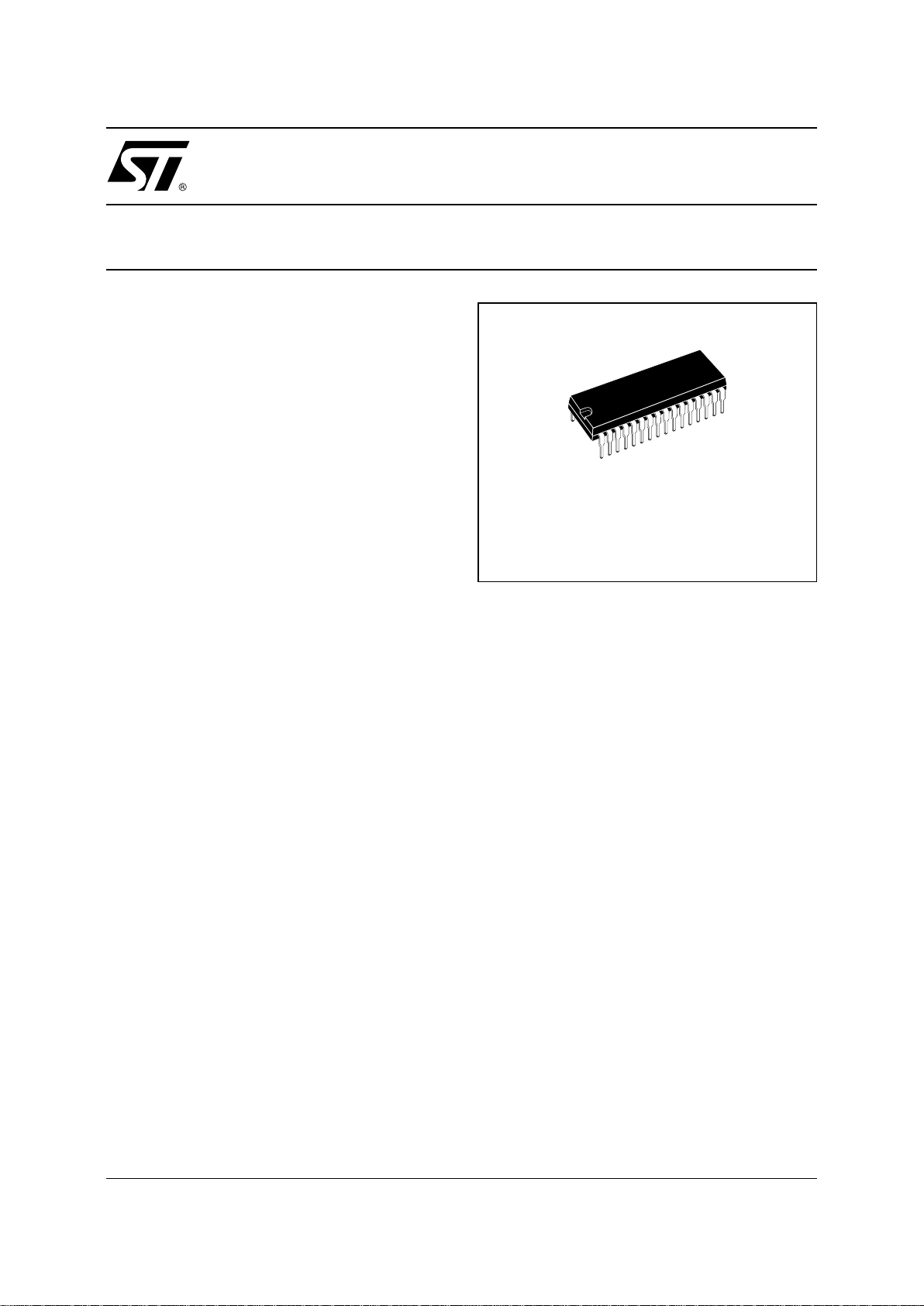
SHRINK32
(Plastic Package)
ORDER CODE : TDA9109/S
HORIZONTAL
.
SELF-ADAPTATIVE
.
DUAL PLL CONCEPT
.
150kHz MAXIMUM FREQUENCY
.
X-RAY PROTECTION INPUT
.
I2C CONTROLS :
HORIZONTAL DUTY-CYCLE, H-POSITION,
FREE RUNNING FREQUENCY, FREQUENCY
GENERATOR FOR BURN-IN MODE
VERTICAL
.
VERTICAL RAMP GENERATOR
.
50 TO 185Hz AGC LOO P
.
GEOMETRY TRACKING WITH VPOS & VAMP
.
I2C CONTROLS :
VAMP, VPOS, S-CORR, C-CORR
.
DC BREATHING COMPENSATION
I
2
C GEOMETRY CO RRE CTIONS
.
VERTICAL PARABO LA GENERATOR
(Pin Cushion - E/W, Keystone, Corner)
.
HORIZONTAL DYNAMIC PHASE
(Side Pin Balance & Parallelogram)
.
VERTICAL DYN AM IC FOCUS
(Ver tical Focus Amplitude)
GENERAL
.
SYNC PR O CESSOR
.
12V SUPPLY VOL TAGE
.
8V REFERENCE VOLT A G E
.
HOR. & VERT. LOCK/UNLOCK OUTPUTS
.
READ/WRITE I2C INTERFAC E
.
HORIZONTAL AND V ER TIC AL MOI RE
.
B+ REGULATOR
- INTERNAL PWM GENERATOR FOR B+
CURRENT MODE STEP -UP CO NV ER TER
- SOFT START
-I
2
C ADJUSTAB LE B+ REFERENCE VOL T AGE
- OUTPUT PULSES SYNCHRONIZED ON
HORIZONTAL FREQUENCY
- INTERNAL MAXIMUM CURRENT LIMITA TION
.
COMPARED WITH THE TDA9109,
THE TDA9109/S HAS :
- CORNER CORRECTION,
- HORIZONTAL MOIRÉ,
- B+ SOFT START,
- INCREASED MAX. VE RTICAL FREQUENCY,
- NO HORIZONTAL FOCUS,
- NO STEP DOWN OPTION FOR DC/DC CONVERTER.
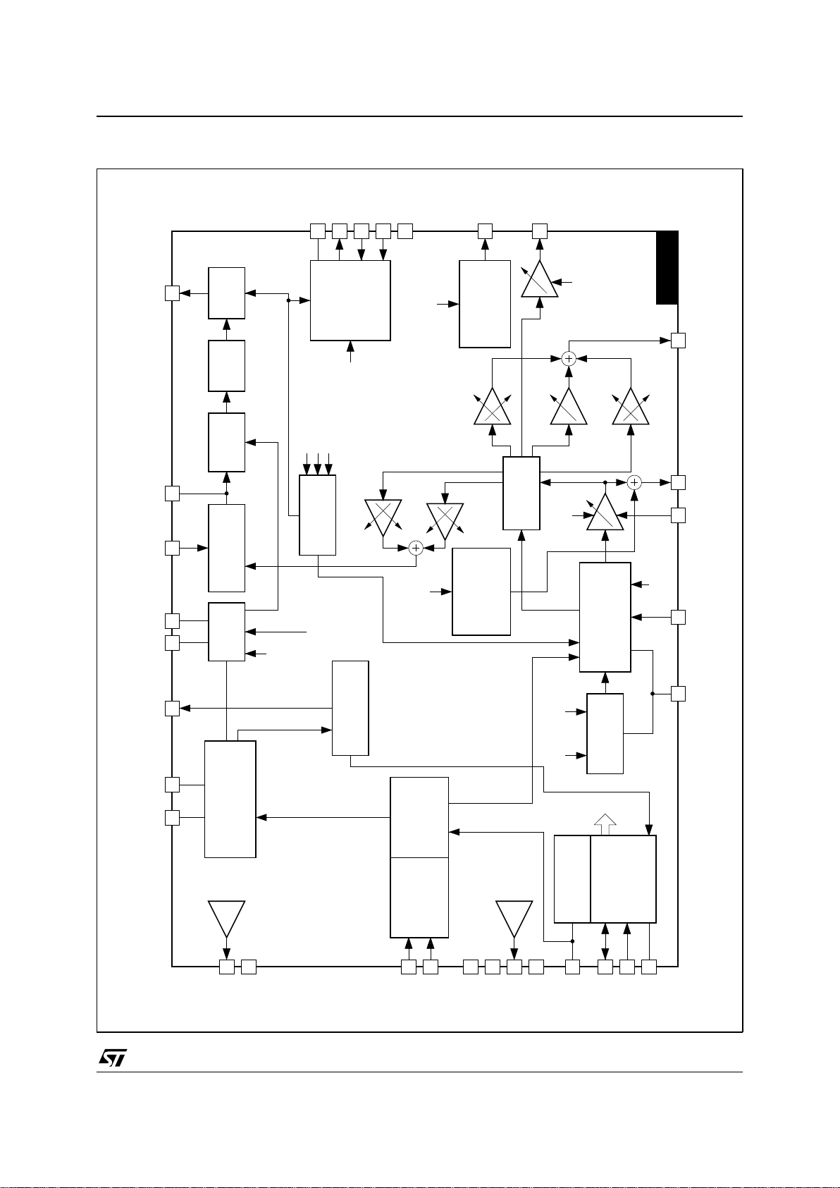
DESCRIPTION
The TDA9109/S is a monolithic integrated circuit
assemb led in 32-pi n shr ink dual i n line pl astic pac kage. This IC controls al l t he functions rela ted t o the
horizontal and vertical deflection in multimode or
multi-frequency comput er dis play monitors .
The intern al sync proc essor , combined with the very
powerful geometry correction block make the
TDA9109/S suitable for very high performance
monitors , u si ng v er y few ex t ern al c omponents.
The horizontal jitter level is very low . It is particularly
well suited for high-end 15" and 17" monitors.
Combined with the ST7275 Microcontroller family, TDA9206 (Video preamplifier) and STV942x
(On-Screen Display controller) the TDA9109/S
allows fully I
2
C bus cont rolled computer di splay
monitors to be built with a reduced number of
external components.
This is advance information on a new product now in development or undergoing evaluation. Details are subject to change without notice.
1/30
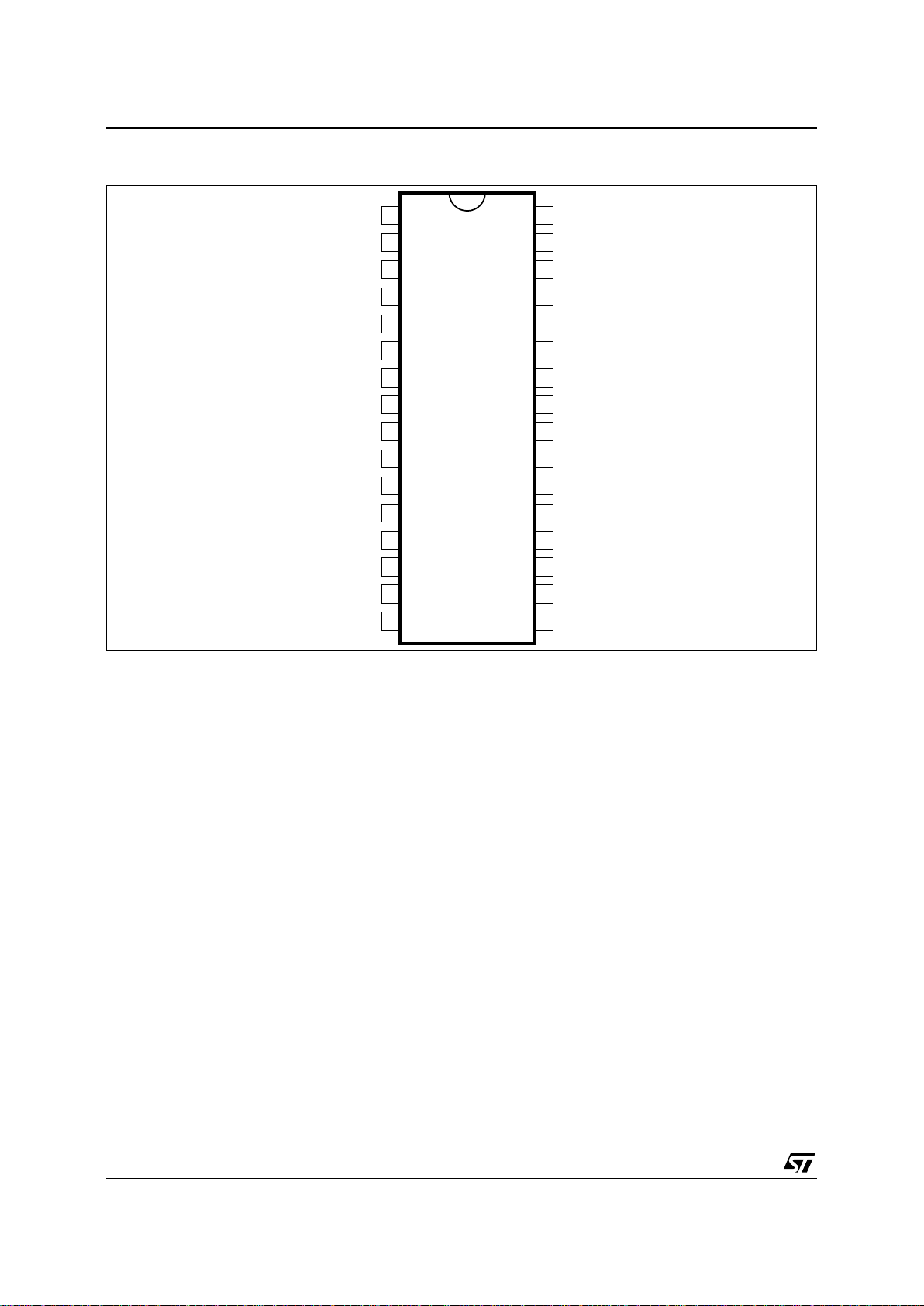
1
2
3
4
5
6
7
8
9
10
11
12
13
14
15
16
22
23
24
25
26
21
20
19
18
17
5V
SDA
SCL
V
CC
GND
HOUT
XRAY
EWOUT
VOUT
VCAP
V
REF
VAGCCAP
VGND
BREATH
B+GNDI
SENSE
REGIN
COMP
HREF
HFLY
HGND
FOCUS-OUT
HMOIRE
HPOSITION
PLL1F
R0
C0
PLL2C
HLOCKOUT
H/HVIN
VSYNCIN
32
31
30
29
28
27
BOUT
9109S-01.EPS
PIN CONNECTIONS
TDA9109/S
2/30
PIN CONNECTIONS
Pin Name Function
1 H/HVIN TTL compatible Horizontal sync Input (separate or composite)
2 VSYNCIN TTL compatible Vertical sync Input (for separated H&V)
3 HLOCKOUT First PLL Lock/Unlock Output (0V unlocked - 5V locked)
4 PLL2C Second PLL Loop Filter
5 C0 Horizontal Oscillator Capacitor
6 R0 Horizontal Oscillator Resistor
7 PLL1F First PLL Loop Filter
8 HPOSITION Horizontal Position Filter (capacitor to be connected to HGND)
9 HMOIRE Horizontal Moiré Output (to be connected to PLL2C through a resistor divider)
10 FOCUSOUT Vertical Dynamic Focus Output
11 HGND Horizontal Section Ground
12 HFLY Horizontal Flyback Input (positive polarity)
13 HREF Horizontal Section Reference Voltage (to be filtered)
14 COMP B+ Error Amplifier Output for frequency compensation and gain setting
15 REGIN Regulation Input of B+ control loop
16 I
SENSE
Sensing of external B+ switching transistor current
17 B+GND Ground (related to B+ reference adjustment)
18 BREATH DC Breathing Input Control (compensation of vertical amplitude against EHV variation)
19 VGND Vertical Section Ground
20 VAGCCAP Memory Capacitor for Automatic Gain Control Loop in Vertical Ramp Generator
21 V
REF
Vertical Section Reference Voltage (to be filtered)
22 VCAP Vertical Sawtooth Generator Capacitor
23 VOUT Vertical Ramp Output (with frequency independant amplitud e and S or C Corrections if any).
It is mixed with vertical position voltage and vertical moiré.
24 EWOUT Pin Cushion - E/W Correction Parabola Output
26 HOUT Horizontal Drive Output (internal transistor, open collector)
25 XRAY X-RAY protection input (with internal latch function)
27 GND General Ground (referenced to V
CC
)
28 BOUT B+ PWM Regulator Output
29 V
CC
Supply Voltage (12V typ)
30 SCL I
2
C Clock Input
31 SDA I
2
C Data Input
32 5V Supply Voltage (5V typ.)
9109S-01.TBL
TDA9109/S
3/30
QUICK REFERENCE DATA
Parameter Value Unit
Horizontal Frequency 15 to 150 kHz
Autosynch Frequency (for given R0 and C0) 1 to 4.5 f0
± Horizontal Sync Polarity Input YES
Polarity Detection (on both Horizontal and Vertical Sections) YES
TTL Composite Sync YES
Lock/Unlock Identification (on both Horizontal 1st PLL and Vertical Section) YES
I
2
C Control for H-Position ± 10 %
XRAY Protection YES
I
2
C Horizontal Duty Cycle Adjust 30 to 60 %
I
2
C Free Running Frequency Adjustment 0.8 to 1.3 f0
Stand-by Function YES
Dual Polarity H-Drive Outputs NO
Supply Voltage Monitoring YES
PLL1 Inhibition Possibility NO
Blanking Outputs NO
Vertical Frequency 35 to 200 Hz
Vertical Autosync (for 150nF on Pin 22 and 470nF on Pin 20) 50 to 185 Hz
Vertical S-Correction YES
Vertical C-Correction YES
Vertical Amplitude Adjustment YES
DC Breathing Control on Vertical Amplitude YES
Vertical Position Adjustment YES
East/West (E/W) Parabola Output (also known as Pin Cushion Output) YES
E/W Correction Amplitude Adjustment YES
Keystone Adjustment YES
Corner Correction YES
Internal Dynamic Horizontal Phase Control YES
Side Pin Balance Amplitude Adjustment YES
Parallelogram Adjustment YES
Tracking of Geometric Corrections with Vertical Amplitude and Position YES
Reference Voltage (both on Horizontal and Vertical) YES
Vertical Dynamic Focus YES
I
2
C Horizontal Dynamic Focus Amplitude Adjustment NO
I
2
C Horizontal Dynamic Focus Symmetry Adjustment NO
I
2
C Vertical Dynamic Focus Amplitude Adjustment YES
Detection of Input Sync Type YES
Vertical Moiré Output YES
Horizontal Moiré Output YES
I
2
C Controlled Moiré Amplitude YES
Frequency Generator for Burn-in YES
Fast I
2
C Read/Write 400 kHz
B+ Regulation adjustable by I
2
C YES
B+ Soft Start YES
9109S-02.TBL
TDA9109/S
4/30
V
REF
4
131211
53
1
67 26
2
HSYNC
HORIZONTAL
MOIRE CANCEL
5 BITS+ON/OFF
9
HMOIRE
HREF
HGND
SYNC
PROCESSOR
SYNC INPUT
SELECT
(1 bit)
B+
CONTROLLER
LOCK/UNLOCK
IDENTIFICATION
PHASE
COMPARATOR
PHASE
SHIFTER
H-DUTY
(5 bits)
HOUT
BUFFER
VCO
Forced
Frequency
2 bits
Free Running
5 bits
VAMP
7 bits
21
22 23
30
19
24
32
31
27
V
REF
VGND
5V
SDA
SCL
GND
V
REF
S AND C
CORRECTION
VERTICAL
OSCILLATOR
RAMP GENERATOR
GEOMETRY
TRACKING
6 bits 6 bits
Keyst.
6 bits
E/W
7 bits
TDA9109/S
PLL1F
HLOCKOUT
HPOSITION
R0
C0
HFLY
PLL2C
HOUT
V
CAP
V
AGCCAP
V
OUT
VSYNCIN
H/HVIN
EWOUT
X
2
X
25
29
XRAY
V
CC
RESET
GENERATOR
I
2
C INTERFACE
VPOS
7 bits
20
AMPVDF
6 bits
10
FOCUS
Parallelogram
6 bits
Spin Bal
6 bits
X
2
X
VSYNC
SAFETY
PROCESSOR
XRAY
V
CC
17
BGND
16
I
SENSE
15
REGIN
28
B+OUT
14
COMP
B+ Adjust
7 bits
18
BREATH
PHASE/FREQUENCY
COMPARATOR
H-PHASE (7 bits)
8
VERTICAL
MOIRE
CANCEL
5 BITS+ON/OFF
5V
Corner
7 bits
X
4
9109S-02.EPS
BLOCK DIAGRAM
TDA9109/S
5/30
ABSOL UT E MAXIMUM RATINGS
Symbol Parameter Value Unit
V
CC
Supply Voltage (Pin 29) 13.5 V
V
DD
Supply Voltage (Pin 32) 5.7 V
V
IN
Max Voltage on Pin 4
Pin 5
Pins 6, 7, 8, 14, 15, 16, 20, 22
Pins 9, 10, 18, 23, 24, 25, 26, 28
Pins 1, 2, 3, 30, 31
4.0
6.4
8.0
V
CC
V
DD
V
V
V
V
V
VESD ESD susceptibility Human Body Model,100pF Discharge through 1.5kΩ
EIAJ Norm, 200pF Discharge through 0Ω
2
300
kV
V
T
stg
Storage Temperature -40, +150
o
C
T
j
Junction Temperature +150
o
C
T
oper
Operating Temperature 0, +70
o
C
9109S-03.TBL
THERMAL DATA
Symbol Parameter Value Unit
R
th (j-a)
Junction-Ambient Thermal Resistance Max. 65
o
C/W
9109S-04.TBL
SYNC PROC ESSOR
Operating Conditions
(V
DD
= 5V , T
amb
= 25oC)
Symbol Parameter Test Conditions Min. Typ. Max. Unit
HsVR Voltage on H/HVIN Input Pin 1 0 5 V
MinD Minimum Horizontal Input Pulses Duration Pin 1 0.7 µs
Mduty Maximum Horizontal Input Signal Duty Cycle Pin 1 25 %
VsVR Voltage on VSYNCIN Pin 2 0 5 V
VSW Minimum Vertical Sync Pulse Width Pin 2 5 µs
VSmD Maximum Vertical Sync Input Duty Cycle Pin 2 15 %
VextM Maximum Vertical Sync Width on TTL H/Vcomposite Pin 1 750 µs
I
HLOCKOUT
Sink and Source Current Pin3 250 µA
Electrical Characteristics
(V
DD
= 5V, T
amb
= 25oC)
Symbol Parameter Test Conditions Min. Typ. Max. Unit
VINTH Horizontal and Vertical Input Logic Level
(Pins 1, 2)
Low Level
High Level 2.2
0.8 V
V
RIN Horizontal and Vertical Pull-Up Resistor Pins 1, 2 200 kΩ
TfrOut Fall and Rise Time, Output CMOS Buffer Pin 3, C
OUT
= 20pF 200 ns
VHlock Horizontal 1st PLL Lock Output Status (Pin 3) Locked, I
LOCKOUT
= -250µA
Unlocked, I
LOCKOUT
= +250µA4.405
0.5 V
V
VoutT Extracted Vsync Integration Time (% of T
H
)
on H/V Composite (see Note 1)
C0 = 820pF 26 35 %
Note 1 :
T
H
is the horizontal period.
I2C READ/WRITE
(see Note 2)
Electrical Characteristics
(V
DD
= 5V,T
amb
= 25oC)
Symbol Parameter Test Conditions Min. Typ. Max. Unit
I
2
C PROCESSOR
Fscl Maximum Clock Frequency Pin 30 400 kHz
Tlow Low period of the SCL Clock Pin 30 1.3 µs
Thigh High period of the SCL Clock Pin 30 0.6 µs
Vinth SDA and SCL Input Threshold Pins 30,31 2.2 V
VACK Acknowledge Output Voltage on SDA input with 3mA Pin 31 0.4 V
Note 2 :
See also I
2
C Table Control and I2C Sub Address Control.
9109S-05.TBL
TDA9109/S
6/30
HORIZONTAL SECTION
Operating Conditions
Symbol Parameter Test Conditions Min. Typ. Max. Unit
VCO
R
0(Min.)
Minimum Oscillator Resistor Pin 6 6 kΩ
C
0(Min.)
Minimum Oscillator Capacitor Pin 5 390 pF
F
(Max.)
Maximum Oscillator Frequency 150 kHz
OUTPUT SECTION
I12m Maximum Input Peak Current Pin 12 5 mA
HOI Horizontal Drive Output Maximum Current Pin 26, Sunk current 30 mA
Electrical Characteristics
(V
CC
= 12V, T
amb
= 25oC)
Symbol Parameter Test Conditions Min. Typ. Max. Unit
SUPPLY AND REFERENCE VOLTAGES
V
CC
Supply Voltage Pin 29 10.8 12 13.2 V
V
DD
Supply Voltage Pin 32 4.5 5 5.5 V
I
CC
Supply Current Pin 29 50 mA
I
DD
Supply Current Pin 32 5 mA
V
REF-H
Horizontal Reference Voltage Pin 13, I = -2mA 7.4 8 8.6 V
V
REF-V
Vertical Reference Voltage Pin 21, I = -2mA 7.4 8 8.6 V
I
REF-H
Max. Sourced Current on V
REF-H
Pin 13 5 mA
I
REF-V
Max. Sourced Current on V
REF-V
Pin 21 5 mA
1st PLL SECTION
HpolT Delay Time for detecting polarity change
(see Note 3)
Pin 1 0.75 ms
V
VCO
VCO Control Voltage (Pin 7) V
REF-H
= 8V f
0
fH(Max.)
1.3
6.2
V
V
Vcog VCO Gain (Pin 7) R
0
= 6.49kΩ, C0 = 820pF,
dF/dV = 1/11R0C
0
17.1 kHz/V
Hph Horizontal Phase Adjustment (see Note 4) % of Horizontal Period ±10 %
Vbmin
Vbtyp
Vbmax
Horizontal Phase Setting Value (Pin 8) (see Note 4)
Minimum Value
Typical Value
Maximum Value
Sub-Address 01
Byte x1111111
Byte x1000000
Byte x0000000
2.8
3.4
4.0
V
V
V
IPll1U
IPll1L
PLL1 Filter Current Charge PLL1 is Unlocked
PLL1 is Locked
±140
±1
µA
mA
f
0
Free Running Frequency
Sub-Address 02 - Byte xxx10000
R0 = 6.49kΩ, C0 = 820pF,
f0 = 0.97/8R0C
0
22.8 kHz
df0/dT Free Running Frequency Thermal Drift
(No drift on external components) (see Note 5)
-150 ppm/C
f
0
(Min.)
f0(Max.)
Free Running Frequency Adjustment
Minimum Value
Maximum Value
Sub-Address 02
Byte xxx11111
Byte xxx00000
0.8
1.3
f0
f0
CR PLL1 Capture Range R
0
= 6.49kΩ, C0 = 820pF,
from f0+0.5kHz to 4.5f
0
f0 adjsusted to 22.8kHz
fH(Min.)
fH(Max.) 100
23.5 kHz
kHz
FF Forced Frequency FF1 Byte 11xxxxxx
FF2 Byte 10xxxxxx
Sub-Address 02 2f0
3f0
Notes :
3. This delay is mandatory to avoid a wrong detection of polarity change in the case of a composite sync.
4. See Figure 10 for explanation of reference phase.
5. These parameters are not tested on each unit. They are measured during our internal qualification.
9109S-05.TBL
TDA9109/S
7/30
HORIZONTAL SECTION
(continued)
Electrical Characteristics
(V
CC
= 12V, T
amb
= 25oC) (continued)
Symbol Parameter Test Conditions Min. Typ. Max. Unit
2nd PLL SECTION AND HORIZONTAL OUTPUT SECTION
FBth Flyback Input Threshold Voltage (Pin 12) 0.65 0.75 V
Hjit Horizontal Jitter At 31.4kHz 70 ppm
HDmin
HDmax
Horizontal Drive Output Duty-Cycle
(Pin 26) (see Note 6)
Sub-Address 00
Byte xxx11111
Byte xxx00000 (see Note 7)
30
60
%
%
XRAYth X-RAY Protection Input Threshold V oltage Pin 25, see Note 8 8 V
Vphi2 Internal Clamping Levels on 2nd PLL
Loop Filter (Pin 4)
Low Level
High Level
1.6
4.0
V
V
VSCinh Threshold Voltage to Stop H-Out,V-Out,
B-Out and Reset XRAY
when V
CC
< VSCinh (see Note 8)
Pin 29 7.5 V
VSDinh Threshold Voltage to Stop H-Out,V-Out,
B-Out and Reset XRAY
when V
DD
< VSDinh
Pin 32 4.0 V
HDvd Horizontal Drive Output (low level) Pin 26, I
OUT
= 30mA 0.4 V
VERTICAL DYNAMIC FOCUS FUNCTION (positive parabola)
HDFDC Bottom DC Output Level R
LOAD
= 10kΩ, Pin 10 2 V
TDHDF DC Output Voltage Thermal Drift (see
Note 5)
200 ppm/C
AMPVDF Vertical Dynamic Focus Parabola
Amplitude with VAMP and VPOS Typical
Min. Byte 000000
Typ. Byte 100000
Max. Byte 111111
Sub-Address 0F
0
0.5
1
V
PP
V
PP
V
PP
VDFAMP Parabola Amplitude Function of VAMP
(tracking between VAMP and VDF) with
VPOS Typ. (see Figure 1 and Note 9)
Sub-Address 05
Byte 10000000
Byte 11000000
Byte 11111111
0.6
1
1.5
V
PP
V
PP
V
PP
VHDFKeyt Parabola Asymetry Function of VPOS
Control (tracking between VPOS and VDF)
with VAMP Max.
Sub-Address 06
Byte x0000000
Byte x1111111
0.52
0.52
V
PP
V
PP
Notes :
5. These parameters are not tested on each unit. They are measured during our internal qualification.
6. Duty Cycle is t he ratio betw een the output tran sistor OFF tim e and the period. The pow er transist or is controlled OF F when the
output transistor is OFF.
7. Initial Condition for Safe Operation Start Up
8. See Figure 14.
9. S and C correction are inhibited so the output sawtooth has a linear shape.
9109S-05.TBL
TDA9109/S
8/30
VERTIC AL SECTION
Operating Conditions
Symbol Parameter Test Conditions Min. Typ. Max. Unit
OUTPUTS SECTION
VEWM Maximum E/W Output Voltage Pin 24 6.5 V
VEWm Minimum E/W Output Voltage Pin 24 1.8 V
R
LOAD
Minimum Load for less than 1% Vertical Amplitude Drift Pin 20 65 MΩ
Electrical Characteristics
(V
CC
= 12V, T
amb
= 25oC)
Symbol Parameter Test Conditions Min. Typ. Max. Unit
VERTICAL RAMP SECTION
VRB Voltage at Ramp Bottom Point V
REF-V
= 8V, Pin 22 2 V
VRT Voltage at Ramp Top Point (with Sync) V
REF-V
= 8V, Pin 22 5 V
VRTF Voltage at Ramp Top Point (without Sync) Pin 22 VRT-0.1 V
VSTD Vertical Sawtooth Discharge Time Pin 22, C
22
= 150nF 70 µs
VFRF Vertical Free Running Frequency
(see Note 10)
C
OSC (Pin 22)
= 150nF
Measured on Pin22
100 Hz
ASFR AUTO-SYNC Frequency (see Note 11) C
22
= 150nF ±5% 50 185 Hz
RAFD Ramp Amplitude Drift Versus Frequency at
Maximum Vertical Amplitude (see Note 5)
C
22
= 150nF
50Hz < f and f < 185Hz
200 ppm/Hz
Rlin Ramp Linearity on Pin 22 (see Note 10) 2.5V < V
27
and V27 < 4.5V 0.5 %
VPOS Vertical Position Adjustment Voltage
(Pin23 - VOUT mean value)
Sub Address 06
Byte x0000000
Byte x1000000
Byte x1111111 3.65
3.2
3.5
3.8
3.3 V
V
V
VOR Vertical Output Voltage
(peak-to-peak on Pin 23)
Sub Address 05
Byte x0000000
Byte x1000000
Byte x1111111 3.5
2.25
3
3.75
2.5 V
V
V
VOI Vertical Output Maximum Current (Pin 23) ±5mA
dVS Max Vertical S-Correction Amplitude
(see Note 12)
x0xxxxxx inhibits S-CORR
x1111111 gives max S-CORR
Sub Address 07
∆V/V
PP
at TV/4
∆V/VPP at 3TV/4
-4
+4
%
%
Ccorr Vertical C-Corr Amplitude
x0xxxxxx inhibits C-CORR
Sub Address 08
∆V/V
PP
@ TV/2
Byte x1000000
Byte x1100000
Byte x1111111
-3
0
3
%
%
%
Notes :
5. These parameters are not tested on each unit. They are measured during our internal qualification.
10. With Register 07 at Byte x0xxxxxx (S correction is inhibited) and with Register 08 at Byte x0xxxxxx (C correction is inhibited), the
sawtooth has a linear shape.
11. This is the frequency range for which the vertical oscillator will automatically synchroniz e, using a single capacitor value on Pin 22
and with a constant ramp amplitude.
12. TV is the vertical period.
9109S-05.TBL
TDA9109/S
9/30

VERTIC AL SECTION
(continued)
Electrical Characteristics
(V
CC
= 12V, T
amb
= 25oC) (continued)
Symbol Parameter Test Conditions Min. Typ. Max. Unit
East/West (E/W) FUNCTION
EW
DC
DC Output Voltage with Typ. VPOS, Keystone and
Corner inhibited
Pin 24, see Figure 2 2.5 V
TDEW
DC
DC Output Voltage Thermal Drift See Note 13 100 ppm/C
EWpara Parabola Amplitude with Max. VAMP, Typ. VPOS,
Keystone and Corner inhibited
Subaddress 0A
Byte 11111111
Byte 11000000
Byte 10000000
1.7
0.85
0
V
PP
V
PP
V
PP
EWtrack Parabola Amplitude Function of VAMP Control
(tracking between VAMP and E/W) with Typ. VPOS,
Typ. E/W Amplitude, Keystone and Cor ner inhibi ted
(see Note 10)
Subaddress 05
Byte 10000000
Byte 11000000
Byte 11111111
0.30
0.55
0.85
V
PP
V
PP
V
PP
KeyAdj Keystone Adjustment Capability with Typ. VPOS,
Corner and E/W inhibited and Max. Vertical
Amplitude (see Note 10 and Figure 4)
Subaddress 09
Byte 1x000000
Byte 1x111111
0.65
0.65
V
PP
V
PP
KeyTrack Intrinsic Keystone Function of VPOS Control
(tracking between VPOS and E/W) with Max. E/W
Amplitude,Max. Vertical Amplitude and Corner
inhibited (see Note 13 and Figure 2)
A/B Ratio
B/A Ratio
Subaddress 06
Byte x0000000
Byte x1111111
0.52
0.52
Corner Corner Amplitude with Max. VAMP, Typ. VPOS,
Keystone and E/W inhibited
Subaddress 0B
Byte 11111111
Byte 11000000
Byte 10000000
1.7
0
-1.7
V
PP
V
PP
V
PP
INTERNAL DYNAMIC HORIZONTAL PHASE CONTROL
SPBpara Side Pin Balance Parabola Amplitude (Figure 3) with
Max. VAMP, Typ. VPOS and Parallelogram inhibited
(see Notes 10 & 14)
Subaddress 0D
Byte x1111111
Byte x1000000
+1.4
-1.4
%T
H
%T
H
SPBtrack Side Pin Balance Parabola Amplitude function of
VAMP Control (tracking between VAMP and SPB)
with Max. SPB, Typ. VPOS and Parallelogram
inhibited (see Notes 10 & 14)
Subaddress 05
Byte 10000000
Byte 11000000
Byte 11111111
0.5
0.9
1.4
%T
H
%T
H
%T
H
ParAdj Parallelogram Adjustment Capability with
Max. VAMP, Typ. VPOS and Max. SPB
(see Notes 10 & 14)
Subaddress 0E
Byte x1111111
Byte x1000000
+1.4
-1.4
%T
H
%T
H
Partrack Intrinsic Parallelogram Function of VPOS Control
(tracking between VPOS and DHPC) with
Max. VAMP, Max. SPB and Parallelogram inhibited
(see Notes 10 & 14)
A/B Ratio
B/A Ratio
Subaddress 06
Byte x0000000
Byte x1111111
0.52
0.52
VERTICAL MOIRE
VMOIRE Vertical Moiré (measured on VOUT : Pin 23) Subaddress 0C
Byte 01x11111 6 mV
BREATHING COMPENSATION
BRRANG DC Breathing Control Range (see Note 15) V18 1 12 V
BRADj Vertical Output Variation versus DC Breathing
Control (Pin 23)
V
18
≥ V
REF-V
V18 = 4V
0
-10
%
%
Notes :
10. With Register 07 at Byte x0xxxxxx (S correction is inhibited) and with Register 08 at Byte x0xxxxxx (C correction is inhibited), the
sawtooth has a linear shape.
13. These parameters are not tested on each unit. They are measured during our internal qualification.
14. T
H
is the horizontal period.
15. When not used the DC breathing control pin must be connected to 12V.
9109S-05.TBL
TDA9109/S
10/30

B+ SECTION
Operating Conditions
Symbol Parameter Test conditions Min. Typ. Max. Unit
FeedRes Minimum Feedback Resistor Resistor between Pins 15 and 14 5 kΩ
Electrical Characteristics
(V
CC
= 12V, T
amb
= 25oC)
Symbol Parameter Test conditions Min. Typ. Max. Unit
OLG Error Amplifier Open Loop Gain At low frequency (see Note 16) 85 dB
I
COMP
Sunk Current on Error Amplifier
Output when BOUT is in safety
condition
Pin 14 (see Figure 14) 0.5 mA
UGBW Unity Gain Bandwidth (see Note 13) 6 MHz
IRI Regulation Input Bias Current Current sourced by Pin 15 (PNP base) 0.2 µA
EAOI Error Amplifier Output Current Current sourced by Pin 14
Current sunk by Pin 14
0.52mA
mA
CSG Current Sense Input Voltage Gain Pin 16 3
MCEth Max Current Sense Input Threshold
Voltage
Pin 16 1.2 V
ISI Current Sense Input Bias Current Current sourced by Pin 16 (PNP base) 1 µA
Tonmax Maximum ON Time of the external
power transistor
% of Horizontal period,
f
0
= 27kHz (see Note 17)
100 %
B+OSV B+ Output Saturation Voltage V
28
with I28 = 10mA 0.25 V
IV
REF
Internal Reference Voltage On error amp (+) input for Subaddress 0B
Byte 1000000
4.8 V
V
REFADJ
Internal Reference Voltage
Adjustment Range
Byte 1111111
Byte 0000000
+20
-20
%
%
t
FB+
Fall Time Pin 28 100 ns
Notes :
13. These parameters are not tested on each unit. They are measured during our internal qualification.
16. These para meters are not test ed on each uni t. They are meas ured during our internal qualificat ion procedure which inc ludes
characterization on batches comi ng from corners of our processes and also temperature characterization.
17. The external power transi stor is OFF during about 400ns.
9109S-05.TBL
HDF
DC
A
B
VDF
AMP
9109S-03.EPS
Figure 1 :
Vertical Dynamic Focus Function
DHPC
DC
A
B
SPB
PARA
9109S-05.EPS
Figure 3 :
Dynamic Horizontal Phase Control
Output
EW
DC
A
B
EW
PARA
9109S-04.EPS
Figure 2 :
E/W Output
Keyadj
9109S-06.EPS
Figure 4 :
Keystone Effect on E/W Output
(PCC and Corner Inhibited)
TDA9109/S
11/30

TYPICAL VERTICAL OUTPUT WAVEFORMS
Function
Sub
Address
Pin Byte Specification Effect on Screen
Vertical Size 05 23
10000000
11111111
Vertical
Position
DC
Control
06 23
x0000000
x1000000
x1111111
V
OUTDC
= 3.2V
V
OUTDC
= 3.5V
V
OUTDC
= 3.8V
Vertical
S
Linearity
07 23
0xxxxxxx
Inhibited
1x111111
Vertical
C
Linearity
08 23
1x000000
1x111111
9109S-06.TBL / 9109S-07.EPS TO 9109S-13.EPS
2.25V
3.75V
V
OUTDC
V
OUTDC
V
PP
D
V
D
V
V
PP
= 4%
V
PP
D
V
D
V
V
PP
= 3%
D
V
V
PP
D
V
V
PP
= 3%
TDA9109/S
12/30

GEOMETRY OUTPUT WAVEFORMS
Function
Sub
Address
Pin Byte Specification Effect on Screen
Keystone
(Trapezoid)
Control
09 24
E/W+ Corner
inhibited
1x000000
1x111111
E/W
(Pin Cushion)
Control
0A 24
Keystone +
Corner
inhibited
10000000
11111111
Corner
Control
0B 24
Keystone+
E/W inhibited
11111111
10000000
Parrallelogram
Control
0E Internal
SPB
inhibited
1x000000
1x111111
Side Pin
Balance
Control
0D Internal
Parallelogram
inhibited
1x000000
1x111111
Vertical
Dynamic
Focus
0F 10
9109S-07.TBL / 9109S-14.EPS TO 9109S-24.EPS
1.7V
2.5V
1.7V
1.4% T
H
3.7V
3.7V
1.4% T
H
1.4% T
H
3.7V
1.4% T
H
3.7V
2V
T
V
2.5V
2.5V
0.65V
0.65V
0V
1.7V
2.5V
TDA9109/S
13/30

I2C BUS ADDRESS TABLE
Slave Address (8C) :
Write Mode
Sub Address Definition
D8 D7 D6 D5 D4 D3 D2 D1
000000000Horizontal Drive Selection / Horizontal Duty Cycle
100000001Horizontal Position
200000010Forced Frequency / Free Running Frequency
300000011Sync Priority / Horizontal Moiré Amplitude
400000100Refresh / B+ Reference Adjustment
500000101Vertical Ramp Amplitude
600000110Vertical Position Adjustment
700000111S Correction
800001000C Correction
900001001E/W Keystone
A00001010E/W Amplitude
B00001011E/W Corner Adjustment
C00001100Vertical Moiré Amplitude
D00001101Side Pin Balance
E00001110Parallelogram
F00001111Vertical Dynamic Focus Amplitude
Slave Address (8D) :
Read Mode
No sub address needed.
TDA9109/S
14/30

D8 D7 D6 D5 D4 D3 D2 D1
WRITE MODE
00
HDrive
0, off
[1], on
Horizontal Duty Cycle
[0] [0] [0] [0] [0]
01
Xray
1, reset
[0]
Horizontal Phase Adjustment
[1] [0] [0] [0] [0] [0] [0]
02
Forced Frequency Free Running Frequency
1, on
[0], off
1, f0 x 2
[0], f0 x 3
[0] [0] [0] [0] [0]
03
Sync
0, Comp
[1], Sep
HMoiré
1, on
[0]
Horizontal Moiré Amplitude
[0] [0] [0] [0] [0]
04
Detect
Refresh
[0], off
B+ Reference Adjustment
[1] [0] [0] [0] [0] [0] [0]
05
Vramp
0, off
[1], on
Vertical Ramp Amplitude Adjustment
[1] [0] [0] [0] [0] [0] [0]
06
Vertical Position Adjustment
[1] [0] [0] [0] [0] [0] [0]
07
S Select
1, on
[0]
S Correction
[1] [0] [0] [0] [0] [0]
08
C Select
1, on
[0]
C Correction
[1] [0] [0] [0] [0] [0]
09
E/W Key
0, off
[1]
E/W Keystone
[1] [0] [0] [0] [0] [0]
0A
E/W Amplitude
[1] [0] [0] [0] [0] [0] [0]
0B
E/W Cor
0, off
[1]
E/W Corner Adjustment
[1]
[0] [0] [0] [0] [0] [0]
0C
Test V
1, on
[0], off
VMoiré
1, on
[0]
Vertical Moiré Amplitude
[0] [0] [0] [0] [0]
0D
SPB Sel
0, off
[1]
Side Pin Balance
[1] [0] [0] [0] [0] [0]
0E
Parallelo
0, off
[1]
Parallelogram
[1] [0] [0] [0] [0] [0]
0F
Test H
1, on
[0], off
Vertical Dynamic Focus Amplitude
[1]
[0] [0] [0] [0] [0]
READ MODE
Hlock
0, on
[1], no
Vlock
0, on
[1], no
Xray
1, on
[0], off
Polarity Detection Sync Detection
H/V pol
[1], negative
V pol
[1], negative
Vext det
[0], no det
H/V det
[0], no det
V det
[0], no det
[ ] initial value
Data is transferred with vertical sawtooth retrace.
We recommend to set the unspecified bit to [0] in order to assure the compatibility with future devices.
I
2
C BUS ADDRESS TABLE
(continued)
TDA9109/S
15/30

OPERA TING DESCRIPTION
I - GENERAL CONSIDERATIONS
I.1 - Power Supply
The typical values of the power supply voltages
V
CC
and VDD are 12V and 5V respectively. Opti-
mum operation is obtained for V
CC
between 10.8
and 13.2V and V
DD
between 4.5 and 5.5V.
In order t o avoid erratic o peration of the c ircuit during
the transi ent phase of VCC and VDD switching on, or
off, the value of V
CC
and VDD are moni to re d : if V
CC
is less than 7 .5V typ. or if VDD is less than 4 .0V ty p.,
the outputs of the c ir c uit ar e inh ibited.
Similarly , before VDD reaches 4V , all the I2C register
are reset to their default value.
In order to have very good power supply rejection,
the circuit is internally supplied by several voltage
references (typ. value : 8V). Two of these voltage
references are externally accessible, one for the
vertical and one for the horiz ontal part . They can be
used to bias external circuitry (if I
LOAD
is less than
5mA). It is necess ary to fi lter the voltag e refere nces
by external c apacitors connec ted to ground, in order
to minimize the noise and consequently the "jitter"
on vertica l and horizontal out pu t signals.
I.2 - I
2
C Control
TDA9109/S belongs to the I
2
C controlled device
family. Instead of being controlled by DC voltages
on dedicated control pins, each adjustment can be
done via the I
2
C Interface.
The I
2
C bus is a serial bus with a clock and a data
input. The general function and the bus protocol are
specified in the Philips-bus data sheets.
The interface (Data and Clock) is a comparator with
hysteresis ; the thresholds (less then 2.2V on rising
edge, more than 0.8V on falling edge with 5V
supply) are TTL-compatible. Spikes of up to 50ns
are filtered by an integrator and the maximum clock
speed is limited to 400kHz.
The data line (SDA) can be used bidirectionally.
In read-mode the IC sends reply information
(1 byte) to the micro-processor.
The bus protocol prescribes a full-byte transmission in all cases. The first byte after the start
condition is used to transmit the IC-address
(hexa 8C for write, 8D for read).
I.3 - Write Mode
In write mode the second byte sent contains the
subaddress of the selected function to adjust (or
controls to affect) and the third byte the corresponding data byte. It is possible to send more than one
data byte to the IC. If after the third byte no s top or
start condition is detected, t he circuit increments
automatically by one the momentary subaddress in
the subaddress counter (auto-increment mode).
So it is possible to transmit immediately the following data bytes without sending the IC address or
subaddress. This can be useful to reinitialize all the
controls very quickly (flash manner). This procedure can be finished by a stop condition.
The circuit has 16 adjustment capabilities : 3 for the
horizontal part, 4 for the vertical, 2 for the E/W
correction, 2 for the dynamic horizontal phase control,1 for the Moiré option, 3 for the horizontal and
the vertical dynamic focus and 1 for the B+ reference adjustment.
17 bits are also dedicated to several controls
(ON/OFF, Horizontal Forced Frequency, Sync Priority, Detection Refresh and XRA Y reset).
I.4 - Read Mode
During the read mode the second byte transmits
the reply information.
The reply byte contains the horizontal and vertical
lock/unlock status, the XRA Y activation status and,
the horizontal and vertical polarity detection. It also
contains the sync detection status which is used by
the MCU to assign the sync priority .
A stop condition alway s stops all the activities of the
bus decoder and switches to high impedance both
the data and clock line (SDA and SCL).
See I
2
C subaddress and control tables.
I.5 - Sync Processor
The internal sync processor allows the TDA9109/S
to accept :
- separated horizontal & vertical TTL-compatible
sync signal,
- composite horizontal & vertical TTL-compatible
sync signal.
TDA9109/S
16/30

I.6 - Sync Identification Status
The MCU can read (address read mode : 8D) the
status register via the I
2
C bus, and then select the
sync priority depending on this status.
Among other data this register indicates the pres-
ence of sync pulses on H/HVIN, VSYNCIN and
(when 12V is supplied) whether a Vext has been
extracted from H/HVIN. Both horizontal and vertical
sync are detected even if only 5V is supplied.
In order to choose the right sync priority the MCU
may proceed as follows (see I
2
C Address T able) :
- refresh the status register,
- wait at least for 20ms (Max. vertical period),
- read this status register.
Sync priority choice should be :
Vext
det
H/V
detVdet
Sync priority
Subaddress
03 (D8)
Comment
Sync type
No Yes Yes 1 Separated H & V
Yes Yes No 0 Composite TTL H&V
Of course, when the choice is made, we can refresh
the sync detections and verify that the extracted
Vsync is present and that no sync type change has
occured. The sync processor also gives sync polarity information.
I.7 - IC status
The IC can inform the MCU about the 1st horizontal
PLL and vertical section status (locked or not) and
about the XRAY protection (activated or not).
Resetting the XRAY internal latch can be done
either by decreasing the V
CC
or VDD supply or
directly resetting it via the I
2
C interface.
I.8 - Sync Inputs
Both H/HVIN and VSYNCIN inputs are TTL compatible triggers with hysterisis to avoid erratic
detection. Both inputs inc lude a pull up resistor
connected to V
DD
.
I.9 - Sync Processor Output
The sync processor indicates on the HLOCKOUT
Pin whether 1st PLL is locked to an incoming
horizontal sync. HLOCKOUT is a TTL compatible
CMOS output. Its level goes to high when locked.
In the same time the D8 bit of the s tatus register is
set to 0 .
This information is mainly used to trigger safety
procedures (like reducing B+ value) as soon as a
OPERA TING DESCRIPTION
(continued)
Z
T
Z
9109S-25.EPS
Figure 5
dd
C
TRAMEXT
9109S-26.EPS
Figure 6
change is detected on the incoming sync. Further
to this, it may be used in an automatic procedure
for free running frequency (f0) adjustment :
Sending the desired f0 on the sync input and
progressively decreasing the free running frequency I
2
C register value (address 02), the
HLOCKOUT Pin will go high as soon as t he proper
setting is reached.
Setting the free running frequency this way allows
to fully exploit the TDA9109/S horizontal frequency
range.
II - HORIZONT AL PART
II.1 - Inte rn a l Input Conditions
A digital signal (horizontal sync pulse or TTL
composite) i s sent by the sync pro cessor to the
horizontal input. It may be positive or negative
(see Figure 5).
Using internal integration, both signals are recognized if Z/T < 25%. Synchronization occurs on the
leading edge of the internal sync signal. The minimum value of Z is 0.7µs.
Another integration is able to extract the vertical
pulse from composite sync if the duty cycle is higher
than 25% (typically d = 35%) (see Figure 6).
The last feature performed is the removal of equalization pulses to avoid parasitic pulses on the phase
comparator (which would be disturbed by missing
or extraneous pulses).
TDA9109/S
17/30

6
7
PLL1F
(Loop Filter)
R0
1.6V
6.4V
5
C0
6.4V
1.6V
0 0.875T
HTH
RS
FLIP FLOP
(1.3V < V < 6V)
7
I
0
2
4
I
0
I
0
(0.80 < a < 1.30)
a
I
2
C Free Running
Adjustment
9109S-29.EPS
Figure 9 :
Details of VCO
LOCKDET
COMP1
INPUT
INTERFACE
H/HVIN
High
CHARGE
PUMP
Low
PLL
INHIBITION
VCO
7 6 5
PLL1F R0 C0
PHASE
ADJUST
E2
I2C
HPOS
Adj.
OSC
Tramext
Tramext
I
2
C
Forced
Frequency
Lock/Unlock
Status
8
HPOSITION
1
9109S-28.EPS
Figure 8 :
Block Diagram
OPERA TING DESCRIPTION
(continued)
7
PLL1F
1
m
F
4.7
m
F
1.8k
W
9109S-27.EPS
Figure 7II.2 - PLL1
The P LL1 con sists of a phas e compar ator , an external filter an d a v olt ag e- co nt ro lled os ci llator (VCO).
The phase comp ar at or is a " phas e fre que ncy" type
designed i n CMOS technol ogy. This kind of phase
detector avoids lo cking on wrong freq uencies. It is
followed by a "charge pump", composed of two
current sources : sunk and sourced (typically I = 1mA
when locked and I = 140µA when unlock ed). This
diff erence be tween loc k/unlock allows sm ooth catc hing of the ho rizon t al fr eque ncy by PLL1. This eff ect
is reinforced by an internal original slow down system
when PLL1 is locked, avoiding the horizontal frequency changing too quickly.
The dynamic behaviour of PLL1 is fixed by an external filter whi ch integr ates the curre nt of the charge
pump. A "CRC" filter is generally used (see Figure 7).
The PLL1 is internally inhibited during extracted
vertical sync (if any) to avoid taking in account
missin g pulses or wrong puls es on pha se compa rator.The inhibition is done by a switch located between the char ge pump and the filter (se e Figure 8).
The VCO uses an external RC network. It delivers
a linear sawtooth obtained by the charge and the
discharge of the capacitor, with a current proportional to the current in the resistor. The typical
thresholds of the sawtooth are 1.6V and 6.4V.
The control voltage of the VCO is between 1.33V
and 6V (see Figure 9). The theorical frequency
range of this VCO is in t he ratio of 1 to 4.5. T he
effective frequency range has to be smaller (1 to
4.2) due to clamp intervention on t he filter lowest
value. To remove the device and external components spread, it is possible to adjust the free running frequency through I
2
C. This adjustment can
be done automatically on the manufacturing line
without manual operation by using Hlock/unlock
information. The adjustment range is 0.8 to 1.3 f0
(where 1.3 f0 is the free running frequency at power
on reset).
TDA9109/S
18/30

OPERA TING DESCRIPTION
(continued)
H Osc
Sawtooth
H Drive
1.6V
4.0V
6.4V
7/8T
H
1/8T
H
Ts
Duty Cycle
Internally
Shaped
Flyback
Flyback
9109S-31.EPS
The duty cycle of H-drive is adjustable between 30% and 60%.
Figure 11 :
PLL2 Timing Diagram
H Osc
Sawtooth
Phase REF1
H Synchro
1.6V
Vb
6.4V
2.8V < Vb < 4.0V
7/8T
H
1/8T
H
Phase REF1 is obtained by comparison between the sawtooth and
a DC voltage adj ustable betw een 2.8V and 4.0V. The PLL1 ensures the e xact coi ncidence between t he si gnal phase R EF an d
HSYNC. A ± TH/10 phase adjustment is possible.
9109S-30.EPS
Figure 10 :
PLL1 Timing Diagram
The sync frequency must alw ays be highe r than the
free running frequency. For ex am p le, w hen using a
sync range between 24kHz and 100kHz, the suggested fre e ru nni ng f re que nc y is 23 k Hz .
Another feature is the capability for the MCU to
force the horizontal frequency through I
2
C to 2xf0
or 3xf0 (for burn-in mode or safety requirements).
In this case, the inhibition switch is opened, leav ing
PLL1 free, but the voltage on PLL1 filter is forced
to 2.66V (for 2xf0) or 4.0V (for 3xf0).
PLL1 ensures the coincidence between the leading
edge of the sync signal and a phase reference
obtained by comparison between the sawtooth of
the VCO and an internal DC voltage which is I
2
C
adjustable between 2.8V and 4.0V (corresponding
to ± 10%) (see Figure 10).
The TDA9109/S also includes a Lock/Unlock identification block which senses in real time whether
PLL1 is locked or not on the incoming horizontal
sync signal. The resulting information is available
on HLOCKOUT (see Sync Processor).
When PLL1 is unlocked, it forces HLOCKOUT to
high level.
The lock/unlock information is also available
through the I
2
C read.
II.3 - PLL2
PLL2 ensures a constant position of the shaped
flyback signal in comparison with the sawtooth of
the VCO, taking into account the saturation time T s
(see Figure 11).
The phase comparator of PLL2 (phase type comparator) is followed by a charge pump (typical
output current : 0.5mA).
The flyback input consists of an NPN transistor.
This input must be current driven. The maximum recommended input current is 5mA
(see Figure 12).
The duty cycle is adjustable through I
2
C from 30%
to 60%. For start-up safe operation, the initial duty
cycle (after power-on reset) is 60% in order to avoid
having a too long conduction per iod of the hor izontal scanning transistor.
The maximum storage time (Ts Max.) is (0.44T
H
-
T
FLY
/2). Typically, T
FLY/TH
is around 20% which
means that T s max is around 34% of T
H
.
TDA9109/S
19/30

BOUT
HORIZONTAL
OUTPUT
INHIBITION
VERTICAL
OUTPUT
INHIBITION
S
R
Q
Horizontal Flyback
0.7V
XRAY Protection
V
CC
Checking
V
CC
VCC or VDD off or I2C Reset
XRAY
VSCinh
I
2
C Drive on/off
I
2
C Ramp on/off
VDD Checking
V
DD
VSDinh
9109S-34.EPS
Figure 14 :
Safety Functions Block Diagram
OPERA TING DESCRIPTION
(continued)
II.4 - Output Section
The H-drive signal is sent to the output through a
shaping stage which also controls the H-drive duty
cycle ( I
2
C adjustable) (see Figure 11). In order to
secure the scanning power part operation, the
output is inhibited in the following cases :
- when V
CC
or VDD are too low,
- when the XRAY protection is activated,
- during the Horizontal flyback,
- when the HDrive I
2
C bit control is off.
The output stage consists of a NPN bipolar transistor. Only the collector is accessible (see Figure 13).
This output stage is intended for "reverse" base
control, where setting the output NPN in off-state
will control the power scanning transistor in offstate (see Application Diagram).
The maximum output current is 30mA, and the
corresponding voltage drop of the output V
CEsat
is
0.4V Max.
Obviously the power scanning transistor cannot be
directly driven by the integrated circuit. An interface
has to be added between the circuit and the power
transistor either of bipolar or MOS type.
II.5 - X-RAY Protection
The X-Ray protection is activated by application of
a high level on the X-Ray input (8V on Pin 25).
It inhibits the H-Drive and B+ outputs.
This protection is latched ; it may be reset either by
V
CC
or VDD switch off or by I2C (see Figure 14).
20k
W
Q1
GND 0V
12
HFLY
400
W
9109S-32.EPS
Figure 12 :
Flyback Input Electrical Diagram
H-DRIVE
26
V
CC
9109S-33.EPS
Figure 13
II.6 - Vertical Dynamic Focus
The TDA9109/S delivers a vertical parabola waveform on Pin 10.
This vertical dynamic focus is tracked with VPOS
and V AMP. Its amplitude can be adjusted. It is also
affected by S and C corrections. This positive signal
once amplified is to be sent t o the CRT focusing
grids.
TDA9109/S
20/30

OPERA TING DESCRIPTION
(continued)
III - VERTICAL PART
III.1 - Function
23
VOUT
18
BREATH
VERT_AMP
SUB05/7bits
VMOIRE
SUB0C/5bits
VPOSITION
SUB06/7bits
22
20
SYNCHRO
OSCILLATOR
2
OSC
CAP
DISCH.
VSYNCIN
POLARITY
SAMPLING
SAMPLING
CAPACITANCE
Vlow
Sawth.
Disch.
REF
TRANSCONDUCTANCE
AMPLIFIERCHARGE CURRENT
VS_AMP
SUB07/6bits
COR_C
SUB08/6bits
S CORRECTION
C CORRECTION
9109S-35.EPS
Figure 15 :
AGC Loop Block Diagram
When the synchronization pulse is not present, an
internal current source sets the free running frequency. For an external capacitor, C
OSC
= 150nF,
the typical free running frequency is 100Hz.
The typical free running frequency can be calcu-
lated by :
f
0
(Hz
)
=
1.5 ⋅ 10
−
5
⋅
1
C
OSC
A negative or positive TTL level pulse applied on
Pin 2 (VSYNC) as well as a TTL composite sync on
Pin 1 can synchronize the ramp in the range
[fmin , fmax]. This frequency range depends on the
external capacitor connected on Pin 22.
A 150nF (±5%) capacitor is recommended for
50Hz to 185Hz applications.
The typical maximum and minimum frequency, at
25
o
C and without any correction (S correction or
C correction), can be calculated by :
f
(Max.)
= 3.5 x f0 and f
(Min.)
= 0.33 x f
0
If S or C corrections are applied, these values are
slighty affected.
If a synchronization pulse is applied, the internal
oscillator is synchonized immediately but its
amplitude chan ges. An interna l corr ection t he n
adjusts it in less than half a second. The top
value of the ramp (Pin 22) is sampled on the
AGC capacitor (Pin 20) at each clock pulse and
a transconductance amplifier modifies the
charge current of the capacitor in such a way to
make the amplit ude ag ain con stant.
The read status register provides the vertical LockUnlock and the vertical sync polarity information.
We recommend the use of an AGC capacitor with
low leakage current. A value lower than 100nA is
mandatory.
A good stability of the internal closed loop is
reached by a 470nF ± 5% capacitor value on
Pin 20 (VAG C).
TDA9109/S
21/30

III.2 - I2C Control Adjustments
S and C correction shapes can then be added to
this ramp. These frequency independent S and C
corrections are generated internally. Their amplitudes are adjustable by their respective I
2
C regis-
ters. They can also be inhibited by their select bits.
Finally, the amplitude of this S and C corrected
ramp can be adjusted by the vertical ramp amplitude control register.
The adjusted ramp is available on Pin 23 (V
OUT
) to
drive an external power stage.
The gain of this stage can be adjusted (±25%)
depending on its register value.
The mean value of this ramp is driven by its own
I
2
C register (vertical position). Its value is
VPOS = 7/16 ⋅ V
REF-V
± 300mV.
Usually VOUT is sent through a resistive divider to
the inverting input of the booster. Since VPOS
derives from V
REF-V
, the bias voltage sent to the
non-inverting input of the booster should also derive from V
REF-V
to optimize the accuracy (see Ap-
plication Diagram).
III.3 - Vertical Moiré
By using the vertical moiré, VPOS can be modulated from frame to frame. This function is intended
to cancel the fringes which appear when line to line
interval is very close to the CRT vertical pitch.
The amplitude of the modulation is controlled by
register VMOIRE on sub-address 0C and can be
switched-off via the control bit D7.
III.4 - Basic Equations
In first approximation, the amplitude of the ramp on
Pin 23 (VOUT) is :
V
OUT
- VPOS = (V
OSC
- V
DCMID
) ⋅ (1 + 0.25 (V
AMP
))
with :
-V
DCMID
= 7/16 ⋅ V
REF
(middle value of the ramp
on Pin 22, typically 3.5V)
-V
OSC
= V22 (ramp with fixed amplitude)
-V
AMP
= -1 for minimum vertical amplitude register
value and +1 for maximum
- VPOS is calculated by : VPOS = V
DCMID
+ 0.3 V
P
with VP equals -1 for minimum vertical position
register value and +1 for maximum
The current available on Pin 22 is :
I
OSC
=
3
8
⋅ V
REF
⋅ C
OSC
⋅
f
with : C
OSC
: capacitor connected on Pin 22 and
f : synchronization frequency.
III.5 - Geometric Corrections
The principle is represented in Figure 16.
Starting from the vertical ramp, a parabola-shaped
current is generated for E/W correction (also known
as Pin Cushion correction), dynamic horizontal
phase control correction, and vertical dynamic Focus correction.
The parabola generator is made by an analog
multiplier, the output current of which is equal to :
∆
I = k ⋅ (V
OUT
- V
DCMID
)
2
where VOUT is the vertical output ramp (typically between 2 and 5V) and V
DCMID
is 3.5V (for V
REF-V
= 8V).
One more multiplier provides a current proportional
to (V
OUT
- V
DCMID
)4 for corner correction.
The VOUT sawtooth is typically centered on 3.5V.
By changing the vertical position, the sawtooth
shifts by ±0.3V.
In order to have good screen geometry for any end
user adjustment, the TDA9109/S has the "geometry tracki ng" feature, which allows generation of a
dissymetric parabola depending on the vertical
position.
Due to the large output stage voltage range (E/W,
Keystone, Corner), the combination of tracking
function with maximum vertical amplitude, maximum or minimum vertical position and maximum
gain on the DAC control may lead to the output
stage saturation. This must be avoided by limiting
the output voltage with apropriate I
2
C registers
values.
For the E/W part and the dynamic horizontal phase
control part, a sawtooth-shaped differential current
in the following form is generated :
∆
I’ = k’ ⋅ (V
OUT
- V
DCMID
)
Then ∆I and ∆I’ are added and converted into
voltage for the E/W part.
Each of the three E/W components, and the two
dynamic horizontal phase controls may be inhibited
by their own I
2
C select bit.
The E/W parabola is available on Pin 24 via an
emitter follower output stage which has to be biased by an external resistor (10kΩ to ground).
Since stable in temperature, the device can be DC
coupled with an external circuitry.
The vertical dynamic focus is available on Pin 10.
The dynamic horizontal phase control drives inter-
nally the H-position, moving the HFLY position on
the horizontal sawtooth in the range of ± 1.4% T
H
both for sid e pin balanc e and par allelo gram.
OPERA TING DESCRIPTION
(continued)
TDA9109/S
22/30

EW Output
EW+ Amp
Keystone
Sidepin Amp
Parallelogram
Dynamic Focus
Sidepin Balance
Output Current
To Horizontal
Phase
V
DCMID
(3.5V)
2
Vertical Ramp VOUT
V.Focus
Amp
Parabola
Generator
V
DCMID
(3.5V)
V
DCMID
(3.5V)
23
24
10
Corner
2
9109S-36.EPS
Figure 16 :
Geometric Corrections Principle
OPERA TING DESCRIPTION
(continued)
III.6 - E/W
EWOUT = 2.5V + K1 (V
OUT
- V
DCMID
)+ K2 (V
OUT
- V
DCMID
)2 + K3 (V
OUT
- V
DCMID
)
4
K1 is adjustable by the keystone I2C register,
K2 is adjustable by the E/W amplitude I
2
C register,
K3 is adjustable by the corner I
2
C register.
III.7 - Dynamic Horizontal Phase Control
I
OUT
= K4 (V
OUT
- V
DCMID
)+ K5 (V
OUT
- V
DCMID
)
2
K4 is adju stable by the parallelogram I2C register,
K5 is adjustable by the side pin balance I
2
C register.
TDA9109/S
23/30

IV - DC/DC CONVERTER PART
OPERA TING DESCRIPTION
(continued)
This unit controls the switch-mode DC/DC converter. It converts a DC constant voltage into the
B+ voltage (roughly proportional to the horizontal
frequency) necessary for the horizontal scanning.
ThisDC/DC converter must be configured in stepup mode. It operates very similarly to the well
known UC3842.
IV.1 - Step-up Mode
Operating Description
- The power MOS is switched-on at the middle of
the horizontal flyback.
- The power MOS is switched-off when its current
reaches a predetermined value. For this purpose,
a sense resistor is inserted in its source. The
voltage on this resistor is sent to Pin16 (I
SENSE
).
- The feedback (coming either from the EHV or
from the flyback) is divided to a voltage close to
4.8V and compared to the internal 4.8V reference
(I
VREF
). The difference is amplified by an error
amplifier, the output of which controls the power
MOS switch-of f curren t .
Main Features
- Switching synchronized on the horizontal frequency,
- B+ voltage always higher than the DC source,
- Current limited on a pulse-by-pulse basis.
The DC/DC converter is disabled :
- when V
CC
or VDD are too low,
- when X-Ray protection is latched,
- directly through I
2
C bus.
When disabled, BOUT is driven t o GND by a 0.5mA
current source. This feature allows to implement
externally a soft start circuit.
161415
V
B+
L
+
C3
C2
1/3
S
S
R
Q
400ns
Inhibit SMPS
28
12V
BOUT
I
SENSE
COMPREGIN
95dB
A
± I
adjust
DAC
7bits
I
2
C
TDA9109/S
1M
W
22k
W
1.2V
1.2V
4.8V ±20%
8V
Inhibit
SMPS
Soft
Start
9109S-37.EPS
Figure 17 :
DC/DC Converter
TDA9109/S
24/30

INTERNAL SCHEMATICS
Pins 1 -2
H/HVIN
VSYNCIN
20k
W
200
W
5V
9109S-38.EPS
Figure 18
5V
3
HLOCKOUT
9109S-39.EPS
Figure 19
4
13
12V
PLL2C
HREF
9109S-40.EPS
Figure 20
5
13
12V
C0
HREF
9109S-41.EPS
Figure 21
6
13 13
12V
HREF HREF
R0
9109S-42.EPS
Figure 22
7
PLL1F
9109S-43.EPS
Figure 23
TDA9109/S
25/30

INTERNAL SCHEMATICS
(continued)
8
12V
HREF
HPOSITION
9109S-44.EPS
Figure 24
9
12V
HMOIRE
5V
9109S-45.EPS
Figure 25
10
FOCUSOUT
12V
12V
9109S-46.EPS
Figure 26
12
13
12V
HREF
HFLY
9109S-47.EPS
Figure 27
14
COMP
9109S-48.EPS
Figure 28
15
REGIN
12V
9109S-49.EPS
Figure 29
TDA9109/S
26/30

INTERNAL SCHEMATICS
(continued)
16
12V
I
SENSE
9109S-50.EPS
Figure 30
18
BREATH
12V
9109S-51.EPS
Figure 31
20
12V
VAGCCAP
9109S-52.EPS
Figure 32
22
VCAP
12V
9109S-53.EPS
Figure 33
23
12V
VOUT
9109S-54.EPS
Figure 34
24
EWOUT
12V
9109S-55.EPS
Figure 35
TDA9109/S
27/30

INTERNAL SCHEMATICS
(continued)
25
12V
XRAY
9109S-56.EPS
Figure 36
HOUT-BOUT
Pins 26-28
12V
9109S-57.EPS
Figure 37
12V
Pins 30-31
SDA - SCL
9109S-58.EPS
Figure 38
TDA9109/S
28/30

APPLICATION DIAGRAMS
TP17
J12
TP13
J11
TP10
TP16
123456789101112
242322212019181716151413
PWM0
PWM1
FBLK
VSYNC
HSYNC
V
DD
PXCK
CKOUT
XTALOUT
XTALIN
PWM2
PWM3PWM4
PWM5
PWM6
PWM7
SCL
SDA
RST
GNDRGBTEST
IC3 - STV9422
X1
8MHz
C37
33pF
C38
33pF
C43
47
m
F
L2
22
m
H
+5V
R30
10k
W
R43
10k
W
C42
1
m
F
TILT
J13
C45
10
m
F
J16 J15
432
1
J14
+5V
R39
4.7k
W
R29
4.7k
W
R42
100
W
R41
100
W
C39
22pF
C40
22pF
SCL
SDA
1 2 3 4 5 6 7 8
910111216 15 14 13
GND
QA
IA
IA
CDA
TA2
TA1V
CC
TB1
TB2
CDBIBIBQBQB
ICC1
MC14528
QA
CC3
47pF
PC1
47k
W
+12V
+12V
+12V
CC4
47pF
+12V
PC2
47k
W
CC1
100nF
CC2
10
m
F
R35
10k
W
R10
10k
W
C25
33pF
HOUT
R8
10k
W
C22
33pF
J8
HFLY
Q1
BC557Q2BC557
R15
1k
W
R17
270k
W
R37
27k
W
+12V
R31
27k
W
R19
270k
W
R38
2.2
W
3W
C11 220pF
R18
39k
W
R33
4.7k
W
R9
470
W
R34
1k
W
J1
E/W
C36
1
m
F
Q3
TIP122
E/W POWER STAGE
TP4 TP3
1
7
5
4
6
2
3
IC1
TDA8172
C10
470
m
F
C8
100nF
-12V
C1
220nFR31.5
W
R5
5.6k
W
R11
220
W
0.5W
R4
1
W
0.5W
C4
100nF
R2
5.6k
W
R40
36k
W
C10
100
m
F
35V
D1
1n4001
C14
470
m
F
C9
100nF
TP6
TP7
3
2
1
J18
V YOKE
J6
J3
J2
+12V
-12V
R1
12k
W
C41
470pF
VERTICAL DEFLECTION STAGE
1
2
3
4
5
6
7
8
9
10
11
12
16
15
14
13
C13 10nF
R36 1.8k
W
C31
4.7
m
F
C17 1mF
24
23
22
21
20
19
18
17
26
25
32
31
30
29
28
27
H/HVIN
VSYNCIN
HLOCKOUT SCL
PLL2C
C0 B+OUT
R0 GGND
PLL1F HOUTCOL
HPOSITION XRAYIN
HMOIRE EWOUT
FOCUS VOUT
HGND VCAP
HFLY VREF
HREF VAGCCAP
COMP VGND
REGIN BREATH
I
SENSE
BGND
IC4
TDA9109/S
TP1
+12V
V
CC
C5
100
m
F
C6
100nF
C49
100nF
HOUT
R53
1k
W
C48
10
m
F
C3
47
m
F
C2
100nF
C12
150nF
C15
470nF
+12V
R52
3.9k
W
+12V
Q4
BC557
Q5
BC547
R58
10
W
L3
22
m
H
C50
10
m
F
C7 22nF
C28
820pF 5%
R23
6.49k
W
1%
C16
C33
100nF
C27
47
m
F
HREF
L4
47
m
H
R24
10k
W
R25
1k
W
J9
DYN
FOCUS
C47
100pF
R50
1M
W
C46
1nF
C51
100nF
R57
82k
W
JP1
R51
1k
W
B+OUT
GND
I
SENSE
REGIN
3
2
1
J19
4
CON4
R49
22k
W
+5V
C30
100
m
F
C32
100nF
L1
22
m
H
+5V
SDA
+5V
R56
560
W
D2
1N4148
J17
HOUT
C60
100nF
R74
10k
W
R77
15k
W
P1
10k
W
+12V
R73
1M
W
R76
47k
W
R75
10k
W
TP8
EHT
COMP
R7 10k
W
R45 33k
W
TP14
()
*
()*Optional
2
W
2k
W
9109S-59.EPS
The difference with standard TDA9109 Application Diagram is the resistor divider 2kΩ/2Ω on
Pin 9 (HMOIRE).
Figure 39 :
Demonstration Board
TDA9109/S
29/30

PMSDIP32.EPS
PACKAGE MECHANICAL DATA
32 PINS - PLASTIC SHRINK DIP
Dimensions
Millimeters Inches
Min. Typ. Max. Min. Typ. Max.
A 3.556 3.759 5.080 0.140 0.148 0.200
A1 0.508 0.020
A2 3.048 3.556 4.572 0.120 0.14 0 0.180
B 0.356 0.457 0.584 0.014 0.018 0.023
B1 0.762 1.016 1.397 0.030 0.04 0 0.055
C 0.203 0.254 0.356 0.008 0.010 0.014
D 27.43 27.94 28.45 1.080 1.100 1.120
E 9.906 10.41 11.05 0.390 0.410 0.435
E1 7.620 8.890 9.398 0.300 0.35 0 0.370
e 1.778 0.070
eA 10.16 0.400
eB 12.70 0.500
L 2.540 3.048 3.810 0.100 0.120 0.150
SDIP32.TBL
Information furnished is believed to be accurate and reliable. However, STMicroelectronics assumes no responsibility for the
consequences of use of such information nor for any infringement of patents or other rights of third parties which may result from
its use. No licence is granted by implication or otherwise under any patent or patent rights of STMicroelectronics. Specifications
mentioned in this publication are subject to change without notice. This publication supersedes and replaces all information
previously supplied. STMicroelectronics products are not authorized for use as critical components in life support devices or sys te ms
without express written approv al of STMi cr oelec troni cs.
The ST logo is a trademark of STMicroele ct ronics
©
1998 STMicroelectronics - All Rights Reserved
Purchase of I
2
C Components of STMicroelectronics, conveys a license under the Philips I2C Pate n t .
Rights to use these components in a I
2
C system, is granted provided that the system conforms to
the I
2
C Standard Specifications as defined by Phili ps.
STMicroelectronics GROUP OF COMPANIES
Australia - Brazil - Canada - China - France - Germany - Italy - Japan - Korea - Malaysia - Malta - Morocco- The Netherlands
Singapore - Spain - Sweden - Switzerland - Taiwan - Thailand - United Kingdom - U.S.A.
TDA9109/S
30/30
 Loading...