

TDA9106
LOW COST DEFLECTION PROCESSOR
FOR MULTISYNCMONITORS
PRELIMINARY DATA
HORIZONTAL
.
SELF-ADAPTATIVE
.
DUALPLLCONCEPT
.
150kHzMAXIMUMFREQUENCY
.
X-RAYPROTECTION INPUT
.
I2C CONTROLS: HORIZONTALDUTY-CYCLE,
H-POSITION, FREE RUNNING FREQUENCY,
FREQUENCY GENERATOR FOR BURN-IN
MODE
VERTICAL
.
VERTICALRAMP GENERATOR
.
50 TO165HzAGC LOOP
.
GEOMETRYTRACKINGWITHV-POS & AMP
.
I2C CONTROLS :
V-AMP,V-POS,S-CORR, C-CORR
2
C GEOMETRYCORRECTIONS
I
.
VERTICALPARABOLAGENERATOR
(Pincushion, Keystone, Corner Correction,
Top/bottomCorner Correction Balance)
.
HORIZONTALDYNAMICPHASE
(SidePin Balance & Parallelogram)
.
HORIZONTALAND VERTICALDYNAMIC FOCUS (Horizontal Focus Amplitude, Horizontal
FocusSymmetry)
GENERAL
.
SYNCPROCESSOR
.
HOR.& VERT. SYNC OUTPUT FOR MCU
.
HOR.& VERT. BLANKING OUTPUTS
.
12V SUPPLYVOLTAGE
.
8V REFERENCEVOLTAGE
.
HOR.& VERT. LOCKUNLOCK OUTPUTS
.
READ/WRITEI2C INTERFACE
.
HORIZONTALMOIREOR DAC OUTPUT
DESCRIPTION
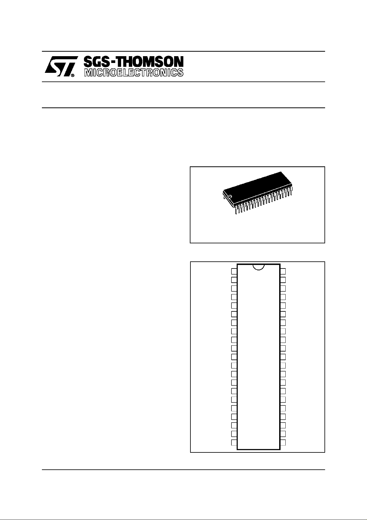
The TDA9106 is a monolithicintegratedcircuit assembledin 42 pinsshrunkdual in line plasticpackage.This IC controlsall thefunctionsrelatedtothe
horizontaland vertical deflection in multimodes or
multi-frequencycomputerdisplaymonitors.
Theinternalsyncprocessor,combinedwiththevery
powerfulgeometrycorrectionblock are making the
TDA9106suitablefor very highperformancemonitorswith veryfewexternalcomponents.
Itisparticularlywellsuitedforhigh-end15”and17”
monitors.
Combined with ST7275 Microcontroller family,
TDA9206 (Video preamplifier) and STV942x
(On-Screen Display controller) the TDA9106
allows to built fully I
display monitors, thus reducing the numberof
external components to a minimum value.
ORDER CODE :
PIN CONNECTIONS
S/G
MOIRE
PLL1INHIB
PLL2C
HREF
HFLY
HGND
FC2
FC1
C0
R0
PLL1F
HLOCKCAP
HPOS
XRAY
HFOCUSCAP
HFOCUS
V
CC
GND
HOUTEM
HOUTCOL
2
C buscon trolledcompute r
SHRINK42
(Plastic Package)
TDA9106
1
2
3
4
5
6
7
8
9
10
11
12
13
14
15
16
17
18
19
20
21 22
42 GND
41
SDA
40
SCL
39
5V
38
H/HVIN
37
HLOCKOUT
36
HOUT
35
VSYNCOUT
34
TEST
33
VSYNCIN
32
VFOCUS
31
EWOUT
30
VFLY
29
VOUT
28
VDCOUT
27
VCAP
26
V
REF
VAGCCAP
25
VGND
24
VBLKOUT
23
HBLKOUT
9106-01.EPS
November 1997
This is advanceinformation on a newproduct now in developmentor undergoingevaluation. Detailsare subject to changewithout notice.
1/30

TDA9106
PIN CONNECTIONS
Pin Name Function
1 S/G Sync on green input
2 MOIRE Moire output
3 PLL1 INHIB TTL-Compatible input for PLL1 inhibition
4 PLL2C Second PLL Loop Filter
5 HREF Horizontal Section Reference Voltage (to filter)
6 HFLY Horizontal Flyback Input (positive polarity)
7 HGND Horizontal Section Ground
8 FC2 VCO Low Threshold filtering Capacitor
9 FC1 VCO High Threshold filtering Capacitor
10 C0 Horizontal Oscillator Capacitor
11 R0 Horizontal Oscillator Resistor
12 PLL1F First PLL Loop Filter
13 HLOCKCAP First PLL Lock/Unlock Time Constant Capacitor
14 HPOS Horizontal Centering Output (to filter)
15 XRAY X-RAY protection input (with internal latch function)
16 HFOCUSCAP Horizontal Dynamic Focus Oscillator Capacitor
17 HFOCUS Horizontal Dynamic Focus Output
18 V
CC
19 GND General Ground (related to V
20 HOUTEM Horizontal Drive Output (internal transistor emitter)
21 HOUTCOL Horizontal Drive Output (int. trans. open collector)
22 HBLKOUT Horizontal Blanking Output (see activation table)
23 VBLKOUT Vertical Blanking Output (see activation table)
24 VGND Vertical Section Ground
25 VAGCCAP Memory Capacitor for Automatic Gain Control Loop in Vertical Ramp Generator
26 V
REF
27 VCAP Vertical Sawtooth Generator Capacitor
28 V
DCOUT
29 VOUT Vertical Ramp Output(with frequencyindependantamplitude and S or C Correctionsif any)
30 VFLY Vertical Flyback Input (positive polarity)
31 EWOUT East/West Pincushion Correction Parabola Output (with Corner corrections if any)
32 VFOCUS Vertical Dynamic Focus Output
33 VSYNCIN TTL-compatible Vertical Sync Input (for separated H&V)
34 TEST Not to be used - Test pin
35 VSYNCOUT TTL Vertical Sync Output (Extracted VSYNC in case of S/G or TTL Composite HV Inputs)
36 HOUT TTL Horizontal Sync Output (To be used for frequency measurement)
37 HLOCKOUT First PLL Lock/Unlock Output (5V unlocked - 0V locked)
38 H/HVIN TTL-compatible Horizontal Sync Input
39 5V Supply Voltage (5V Typ.)
40 SCL I
41 SDA I
42 GND Ground (Related to 5V)
Supply Voltage (12V Typ)
)
CC
Vertical Section Reference Voltage (to filter)
Vertical Position Reference Voltage Output
2
C-Clock input
2
C-Data input
9106-01.TBL
2/30
TDA9106
QUICK REFERENCE DATA
Parameter Value Unit
Horizontal Frequency 15 to 150 kHz
Autosynch Frequency (for given R0 and C0) 1 to 4.5 FH
± Horizontal Sync Polarity Input YES
Polarity Detection (on both Horizontal and Vertical Sections) YES
TTL Composite Synch or Sync on Green YES
Lock/Unlock Identification (on both Horizontal 1st PLL and Vertical Section) YES
2
C Controlfor H-Position ± 10 %
I
XRay Protection YES
2
C Horizontal Duty Adjust 30 to 60 %
I
2
C Free Running Adjustment 0.8 to 1.3 F0
I
Stand-by Function YES
Two Polarities H-Drive Outputs YES
Supply Voltage Monitoring YES
PLL1 Inhibition Possibility YES
Blanking Outputs (both Horizontal and Vertical) YES
Vertical Frequency 35 to 200 Hz
Vertical Autosync (for 150nF) 50 to 165 Hz
Vertical S-Correction YES
Vertical C-Correction YES
Vertical Amplitude Adjustment YES
Vertical Position Adjustment YES
East/West Parabola Output YES
Pin Cushion Correction Amplitude Adjustment YES
Keystone Adjustment YES
Corner and Corner Balance Adjustments YES
Internal Dynamic Horizontal Phase Control YES
Side Pin Balance Amplitude Adjustment YES
Parallelogram Adjustment YES
Tracking of Geometric Corrections YES
Reference Voltage (both on Horizontal and Vertical) YES
Dynamic Focus(both Horizontal and Vertical) YES
2
C Horizontal Dynamic Focus Amplitude Adjustment YES
I
2
C Horizontal Dynamic Focus Keystone Adjustment YES
I
Type of Input Sync Detection (supplied by 5V Digital Supply) YES
Horizontal Moiré Output YES
2
C Controlled H-Moiré Amplitude YES
I
Frequency Generator for Burn-in YES
2
C Read/Write 400 kHz
Fast I
9106-02.TBL
3/30

TDA9106
BLOCKDIAGRAM
HOUTEM
20
HOUTCOL
21
PLL2C
HFLY
FC2
8910
FC1
C0
R0
1112 1314
HLOCKCAP
HLOCKOUT
37
HOUT
BUFFER
(5 bits)
H-DUTY
PHASE
SHIFTER
PHASE
COMPARATOR
VCO
VCCX-RAY
HFOCUS
18
15
SAFETY
PROCESSOR
H-SAWTOOTH
Free Running
2 bits
Safe Freq.
CAP
16
2
X
2 x 5 bits
Amp & Keyst
GENERATOR
Spin Bal
5 bits
6 bits
HFOCUS
2 MOIRE
17
5 BITS
MOIRE
PROCESSOR
2
X
Key Bal
6 bits
CORNER
H-FLY VSYNC
X
SYNC
PROCESSOR
2
6 bits
(2 x 6 bits)
CORRECTION
TRACKING
GEOMETRY
VPOS
X
7 bits
EWOUT
31
X
7 bits
2
X
VERTICAL
OSCILLATOR
RAMP GENERATOR
TDA9106
7 bits
VAMP
32
25
27 28 29
OUT
CAP
V
DCOUT
AGCCAP
V
VFOCUS
V
V
4/30
HPOSFILTER
PLL1F
PLL1INHIB
PHASE/FREQUENCY
3 4
19
GND
COMPARATOR
H-PHASE (7 bits)
REF
V
567
HREF
HGND
LOCK/UNLOCK
IDENTIFICATION
S AND C
SELECT
SYNC INPUT
(2 bits)
6 bits 6 bits
CORRECTION
LOCK
HFLY
C INTERFACE
2
41
SDA
I
40
SCL
42
GND
9106-02.EPS
VSYNC
VFLY
BLANKING
GENERATOR
30
22
VFLY
HBLKOUT
233335
VBLKOUT
VSYNCOUT
36
HOUT
1
S/G
38
H/HVIN
REF
V
26
REF
V
VSYNCIN
24
VGND
RESET GENERATOR
39
34
5V
TEST

TDA9106
ABSOLUTE MAXIMUMRATINGS
Symbol Parameter Value Unit
V
V
V
VESD ESD susceptibility
T
T
THERMAL DATA
Symbol Parameter Value Unit
R
th (j-a)
Supply Voltage (Pin 18) 13.5 V
CC
Supply Voltage (Pin 39) 5.7 V
DD
Max Voltage on Pin 6
IN
Pins 15, 21, 22, 23
Pin 1
Pin 4
Pins 3, 33,34,37,38,40,41
Pin 16
Pins 8, 9, 10, 11, 12, 13, 14, 25, 27, 30
1.8
12
3.6
4
5
6
8
2
Human Body Model,100pF Discharge through 1.5kΩ
EIAJ Norm,200pF Discharge through 0Ω
Storage Temperature -40, +150
stg
Junction Temperature +150
T
j
Operating Temperature 0, +70
oper
300
Junction-ambient Thermal Resistance Max. 65
kV
o
o
o
o
C/W
V
V
V
V
V
V
V
V
C
C
C
9106-03.TBL
9106-04.TBL
SYNCHROPROCESSOR
OperatingConditions
Symbol Parameter Test Conditions Min. Typ. Max. Unit
HsVR Horizontal Sync Input Voltage Pin 38 0 5 V
MinD Minimum Horizontal Input Pulses Duration Pin 38 0.7 µs
Mduty Maximum Horizontal Input Signal Duty Cycle Pin 38 25 %
VsVR Vertical Sync Input Voltage Pin 33 0 5 V
VSW Minimum Vertical Sync Pulse Width Pin 33 5 µs
VSmD Maximum Vertical Sync Input Duty Cycle Pin 33 15 %
VextM Maximum Vertical Sync Width on TTL
H/Vcomposite or S/G
ElectricalCharacteristics
(V
DD
=5V,T
amb
=25oC)
Symbol Parameter Test Conditions Min. Typ. Max. Unit
VSGDC S/G Clamped DC Level Pin 1, I
ISGbias Internal Diode Bias Current Pin 1, V
VSGTh Slicing Level (see application design choice) Pin 1 0.2 V
VINTH Horizontal and Vertical Input Voltage
(Pins 33,38)
RIN Horizontaland Vertical Pull-Up Resistor Pins 33,38 200 kΩ
VOut Output Voltage (Pins 35,36,37) Low level
TfrOut Falling and Rising Output CMOS Buffer Pins 35,36,37
VHlock Horizontal 1st PLL Lock Output Status (Pin37) Locked
VoutT Extracted Vsync Integration Time (% of TH) on
H/V Composite or S/G
Pins 1, 38 750 µs
=-1µA1V
1
= 1.6V 10 µA
1
Low Level
0.8 V
High Level 2.2
0
High Level
5
100 ns
Cout = 20pF
0
Unlocked
5
Pin 35, C0 = 820pF 26 35 %
V
V
V
V
V
9106-05.TBL
5/30
TDA9106
I2C READ/WRITE
ElectricalCharacteristics
Symbol Parameter Test Conditions Min. Typ. Max. Unit
2
I
C PROCESSOR
Fscl Maximum Clock Frequency Pin 40 400 kHz
Tlow Low period of the SCL Clock Pin 40 1.3 µs
Thigh High period of the SCL Clock Pin 40 0.6 µs
Vinth SDA and SCL Input Threshold Pins 40,41 2.2 V
VACK AcknowledgeOutput VoltageonSDAinput with3mA Pin 41 0.4 V
See also I2CTable Controland I2C Sub Address Control
HORIZONTAL SECTION
OperatingConditions
Symbol Parameter Test Conditions Min. Typ. Max. Unit
VCO
R
0(Min.)
C
0(Min.)
F
(Max.)
OUTPUT SECTION
I6m Maximum Input Peak Current Pin 6 2 mA
HOI1
HOI2
Minimum Oscillator Resistor Pin 11 6 kΩ
Minimum Oscillator Capacitor Pin 10 390 pF
Maximum Oscillator Frequency 150 kHz
Horizontal Drive Output Maximum Current
Pin 20
Pin 21
(V
DD
=5V,T
amb
=25oC)
Sourced current
Sunk current
2020mA
mA
ElectricalCharacteristics (VCC=12V,T
amb
=25oC)
Symbol Parameter Test Conditions Min. Typ. Max. Unit
SUPPLY AND REFERENCE VOLTAGES
V
V
I
I
V
REF-H
V
REF-V
I
REF-H
I
REF-V
Supply Voltage Pin 18 10.8 12 13.2 V
CC
Supply Voltage Pin 39 4.5 5 5.5 V
DD
Supply Current Pin 18 50 mA
CC
Supply Current Pin 39 5 mA
DD
Horizontal Reference Voltage Pin 5, I = 5mA 7.4 8 8.6 V
Vertical Reference Voltage Pin 5, I = 5mA 7.4 8 8.6 V
Max. Sourced Current on V
Max. Sourced Current on V
REF-H
REF-V
Pin 5 5 mA
Pin 26 5 mA
9106-05.TBL
6/30

TDA9106
HORIZONTAL SECTION (continued)
ElectricalCharacteristics
Symbol Parameter Test Conditions Min. Typ. Max. Unit
1st PLL SECTION
HpolT Polarity Integration Delay 0.75 ms
V
Vcog VCO Gain(Pin 12) R
Hph Horizontal Phase Adjustment % of Horizontal Period ±10 %
Hphmin
Hphtyp
Hphmax
dF0/dT FreeRunning Frequency Thermal Drift
f
(Min.)
0
(Max.)
f
0
CR PLL1 Capture Range R
PLLinh PLL1 Inhibition (Pin3) Typ Threshold = 1.6V
SFF Safe Forced Frequency
FC1
FC2
2nd PLL SECTION AND HORIZONTAL OUTPUT SECTION
FBth Flyback Input Threshold Voltage (Pin 6) 0.65 0.75 V
Hjit Horizontal Jitter (see Pins 8-9 filtering) TBD ppm
HDmin
HDmax
XRAYth X-RAY Protection Input Threshold Voltage Pin 15 8 V
Vphi2 Internal Clamping Levels on 2nd PLL Loop
VSCinh Threshold Voltage To Stop H-Out,V-Out
IHblk Maximum Horizontal Blanking Output
VHblk Horizontal Blanking Output Low Level
HDvd
HDem
Notes :
VCO Control Voltage (Pin12) V
VCO
Horizontal Phase Decoupling Output
Minimum Value
Typical Value
Maximum Value
Free Running Frequency R0= 6.49kΩ,C0= 820pF,
f
0
(No drift on external components)
Free Running Frequency Adjustment
Minimum Value
Maximum Value
SF1 Byte 11xxxxxx
SF2 Byte 10xxxxxx
VCO SawtoothLevel
High FC1=(4.V
Low FC2=(V
REF-H
Horizontal Drive Output Duty-Cycle
(Pin 20 or 21) (see Note 1)
Low Level
High Level (see Note 2)
Filter (Pin 4)
when V
< VSCinh
CC
Current
(Blanking ON)
Horizontal Drive Output
Low Level (Pin 20 to GND)
High Level (Pin 21 to V
1. Duty Cycle is theratio of power transistorOFF time to period.Power transistor is OFF when output transistor is OFF.
2. Initial Conditionfor Safe Operation Start Up (Max. duty cycle).
(V
REF-H
)/5
CC
)/5
=12V,T
=12V)
CC
=25oC) (continued)
amb
REF-H
f
0
fH(Max.)
= 6.49kΩ,C0= 820pF,
0
dF/dV = 1/11R
Sub-Address 01, Pin 14
Byte x1111111
Byte x1000000
Byte x0000000
= 0.97/8R0C
f
0
Sub-Address 02
Byte xxx11111
Byte xxx00000
= 6.49kΩ,C0= 820pF,
0
from f
fH(Min.)
f
H
PLL ON
PLL OFF 2
Sub-Address 02
Pin 9 To filter
Pin 8 To filter
Sub-Address 00
Byte xxx11111
Byte xxx00000
Low Level
High Level
Pin 18 7.5 V
I
22
V
with I22= 10mA 0.25 0.5 V
22
V
21-V20,IOUT
V
20,IOUT
=8V
0C0
0
+0.5kHz to 4.5F
0
0
(Max.) 100
= 20mA
= 20mA 9.5
V
/6
REF-H
6.2
17 kHz/V
2.8
3.4
4.0
22.3 kHz
-150 ppm/C
0.8
1.3
23.5 kHz
0.8 V
2F0
3F0
6.4
1.6
30
60
1.6
4.0
10 mA
1.1
1.7 V
10
V
V
V
V
V
F0
F0
kHz
V
V
V
%
%
V
V
V
9106-05.TBL
7/30

TDA9106
HORIZONTAL SECTION(continued)
ElectricalCharacteristics
Symbol Parameter Test Conditions Min. Typ. Max. Unit
HORIZONTAL DYNAMIC FOCUS SECTION
HDFst Horizontal Dynamic Focus Sawtooth
HDFdis Horizontal Dynamic Focus Sawtooth
HDFDC Bottom DC Output Level R
TDHDF DC Output Voltage Thermal Drift 200 ppm/C
HDFamp Horizontal Dynamic Focus Amplitude
HDFKeyst Horizontal Dynamic Focus Keystone
MOIRE OUTPUT
R
MOIRE
V
MOIRE
Minimum Level
Maximum Level
Discharge Width
Min Byte xxx11111
Typ Byte xxx10000
Max Byte xxx00000
Min A/B Byte xxx11111
Typ Byte xxx10000
Max A/B Byte xxx00000
Minimum Output Resistor Pin 2 2 kΩ
Output Voltage (moire off),
Subaddress 0F
(V
CC
=12V,T
=25oC) (continued)
amb
HfocusCap = C
= 90kHz, Pin 16 2
f
H
Driven by Hfly 500 ns
= 10kΩ, Pin 17 2 V
LOAD
Sub-Address 03, Pin 17,
= 90kHz, Keystone Typ 1
f
H
Sub-Address 04,
= 90kHz, Typ Amp
f
H
B/A
A/B
A/B
Pin 2, R
Byte 0xx00000
Byte 0xx10000
Byte 0xx11111
MOIRE
= 820pF,
0
=2kΩ
4.7
1.5
3
3.5
1.0
3.5
0.2
1.1
2.0
V
V
V
PP
V
PP
V
PP
V
V
V
9106-05.TBL
8/30

TDA9106
VERTICALSECTION
OperatingConditions
Symbol Parameter Test Conditions Min. Typ. Max. Unit
OUTPUTS SECTION
VEWM Maximum EW Output Voltage Pin 31 6.5 V
VEWm Minimum EW OutputVoltage Pin 31 1.8 V
VDFm Minimum Vertical Dynamic Focus Output Voltage Pin 32 1.8 V
R
LOAD
Minimum Load for less than 1% Vertical Amplitude Drift Pin 25 65 MΩ
ElectricalCharacteristics
(V
CC
=12V,T
amb
=25oC)
Symbol Parameter Test Conditions Min. Typ. Max. Unit
VERTICAL RAMP SECTION
VRB Voltage at Ramp BottomPoint V
VRT Voltage at Ramp Top Point (withSync) V
REF-V
VRTF Voltage at Ramp Top Point (without Sync) Pin 27 VRT-
=8V, Pin27 2 V
REF-V
Pin 27 5 V
V
0.1
VSTD Vertical Sawtooth Discharge Time Duration
With 150nF Cap 80 µs
(Pin 27)
VFRF Vertical Free Running Frequency
(see Notes 3 & 4)
ASFR AUTO-SYNC Frequency C
RAFD Ramp Amplitude Drift Versus Frequency
at Maximum Vertical Amplitude
Rlin Ramp Linearity on Pin 27 (see Notes 3 & 4) 2.5 < V
C
OSC (Pin27)
Measured on Pin27,
27
See Note 5
C
27
50Hz < f and f < 165Hz
= 150nF
= 150nF ±5%
= 150nF
and V27< 4.5V 0.5 %
27
100 Hz
50 165 Hz
200 TBD ppm/Hz
Vpos Vertical Position Adjustment Voltage(Pin28) Sub Address 06
I
VPOS
Max Current on Vertical Position Output Pin 28 ±2mA
VOR Vertical Output Voltage
(peak-to-peak on Pin 29)
Byte x0000000
Byte x1000000
Byte x1111111 3.65
Sub Address 05
Byte x0000000
Byte x1000000
Byte x1111111 3.5
3.2
3.5
3.8
2.25
3
3.75
3.3 V
V
V
2.5 V
V
V
VoutDC DC Voltage on Vertical Output See Note 6, Pin 29 3.5 V
VOI Vertical Output Maximum Current (Pin29) ±5mA
dVS Max Vertical S-Correction Amplitude
x0xxxxxx inhibits S-CORR
x1111111 gives max S-CORR
Ccorr Vertical C-Corr Amplitude
x0xxxxxx inhibits C-CORR
Subaddress 07
PP
PP
at T/4
at 3T/4
∆V/V
∆V/V
SubAddress 08
Byte x1000000
Byte x1100000
Byte x1111111
-4
+4
-3
0
3
%
%
%
%
%
VflyTh Vertical Flyback Threshold Pin 30 1 V
VflyInh Inhibition of Vertical Flyback Input See Note 7, Pin 30 7.5 V
Notes : 3. WithRegister07 at Byte x0xxxxxx(Vertical S-CorrectionControl) thenthe S correctionis inhibited, consequentlythesawtooth has
a linear shape.
4. With Register 08 at Byte x0xxxxxx (Vertical C - Correction Control) then the C correction is inhibited, consequently the sawtooth
has a linear shape.
5. It is the frequency range for which theVERTICAL OSCILLATOR will automaticallysynchronize, using a single capacitor valueon
Pin 27 andwith aconstantramp amplitude.
OUTDC = (7/16).VREF-V. Typically 3.5V forVertical reference voltage typical value (8V).
6. V
7. WhenPin30 ( V
discharge time.
) - 0.5V, Vfly input is inhibitedand vertical blanking onvertical blanking output is replacedby vertical sawtooth
REF-V
9106-05.TBL
9/30

TDA9106
VERTICALSECTION(continued)
ElectricalCharacteristics
Symbol Parameter Test Conditions Min. Typ. Max. Unit
EAST/WEST FUNCTION
EW
TDEW
EWpara Parabola Amplitude with Vamp Max, V-Pos Typ,
EWtrack Parabola Amplitude Function of V-AMP Control
KeyAdj Keystone Adjustment Capability with Typ Vpos,
KeyTrack Intrinsic Keystone Function of V-POS Control
Corner
Max
Corner
BalMax
INTERNAL HORIZONTAL DYNAMIC PHASE CONTROL FUNCTION
SPBpara Side Pin Balance Parabola Amplitude (Figure 2)
SPBtrack Side Pin Balance Parabola Amplitude function of
ParAdj Parallelogram Adjustment Capability with Vamp
Partrack Intrinsic Parallelogram Function of Vpos Control
Notes : 8. These parameters are not tested on each unit. They are measured duringour internalqualification
DC Output Voltage with Typ Vpos,Keystone,
DC
Corner and Corner Balance Inhibited
DC Output Voltage Thermal Drift See Note 8 100 ppm/C
DC
Keystone, Corner and Corner Balance Inhibited
(trackingbetween V-AMP and E/W) withTyp Vpos,
Keystone, Corner and Corner Balance Inhibited,
EW Typ Amplitude (see Note 9)
Cornerand Corner Balance Inhibited, EW Inhibited
and Vertical AmplitudeMax
(see Note 9 and Figure 4)
(trackingbetween V-POS and EW)withCorner and
Corner Balance Inhibited, EW Max Amplitude and
Vertical Amplitude Max (see Note 9)
A/B Ratio
B/A Ratio
Max Corner Correction Amplitude with Vamp Max,
V-P O S T yp, EW a m p, Keyst one a nd Corner
Balance Inhibited (see Note 9)
Max Corner Balance Correction Amplitude with
Vamp Max, V-POS Typ, EWamp, Keystone and
Corner Inhibited
Subaddress 0C (see Note 9)
with Vamp Max, V-POS Typ and Parallelogram
Inhibited (see Notes 9 & 10)
Vamp Control (tracking between Vamp and SPB)
with SPB Max, V-POS Typ and Parallelogram
Inhibited (see Notes 9 & 10)
Max, V-POS Typ and SPB Inhibited
(see Notes 9, 10 & 11)
(tracking between V-Pos and DHPC) with Vamp
Max, SP B M a x an d Parallelogr a m Inhibit ed
(see Notes 9 & 10)
A/B Ratio
B/A Ratio
9. Refers to Notes 3 &4 from last section.
10.TH is the Horizontal PLL PeriodDuration.
11.Figure 2 is representing effect of dynamic horizontal phase control.
(V
CC
=12V,T
=25oC) (continued)
amb
Pin 31, see Figure 1 2.5 V
Subaddress 09
Byte 1x111111
Byte 1x100000
Byte 1x000000
2.6
1.4
0
Subaddress 05
Byte 10000000
Byte 11000000
Byte 11111111
0.45
0.8
1.4
Subaddress 0A
Byte 10000000
Byte 11111111
1
1
Subaddress 06
Byte x0000000
Byte x1111111
0.5
0.5
Subaddress 0B
∆EWout at T/6, 5T/6
Byte x1111111
Byte x1000000
+0.2
-0.2
Byte 01111111
∆EWout at T/4
∆EWout at 3T/4
+0.2
-0.2
Byte 01000000
∆EWout at T/4
∆EWout at 3T/4
-0.2
+0.2
Subaddress 0D
Byte x1111111
Byte x1000000
+2.8
-2.8
Subaddress 05
Byte 10000000
Byte 11000000
Byte 11111111
1.0
1.8
2.8
Subaddress 0E
Byte x1111111
Byte x1000000
+2.8
-2.8
Subaddress 06
Byte x0000000
Byte x1111111
0.5
0.5
V
V
V
V
V
V
V
PP
V
PP
V
V
V
V
V
V
%TH
%TH
%TH
%TH
%TH
%TH
%TH
9106-05.TBL
10/30

TDA9106
VERTICALSECTION(continued)
ElectricalCharacteristics
Symbol Parameter Test Conditions Min. Typ. Max. Unit
VERTICAL DYNAMIC FOCUS FUNCTION
VDF
TDVDF
VDFAMP Parabola Amplitude Function of Vamp (tracking
VDFKEY Parabola Assymetry Function of VPos Control
Notes :
Figure1 :
DC Output Voltage with V-Pos Typ See Figure 3 6 V
DC
DC Output Voltage Thermal Drift See Note 12 100 ppm/C
DC
between Vamp and VDF) with V-Pos Typ
(see Figure 3)(see Note 13)
(trackingbetween V-Pos andVDF) withVampMax.
(see Note 13)
12. Parameter nottested on each unitbutmeasured duringour internal qualificationprocedure includingbatches coming fromcorners
of our process and also temperaturecharacterization
13. S and C corrections are inhibited so theoutput sawtooth has a linear shape.
E/WOutput
(V
CC
=12V,T
=25oC) (continued)
amb
Figure 2 :
Subaddress 05
Byte 10000000
Byte 11000000
Byte 11111111
Subaddress 06
Byte x0000000
Byte x1111111
DynamicHorizontalPhaseControl
Output
0.9
1.6
2.5
0.5
0.5
V
V
V
9106-05.TBL
A
EW
Figure3 :
A
EW
PARA
DC
VerticalDynamic Focus Function
VDF
DC
AMP
B
A
SPB
PARA
9106-03.EPS
Figure 4 :
KeystoneEffecton E/W Output
B
DHPC
DC
9106-04.EPS
(PCCInhibited)
BVDF
9106-05.EPS
Keyadj
9106-06.EPS
11/30

TDA9106
TYPICALVERTICAL OUTPUT WAVEFORMS
Function
Sub
Address
Pin Byte Specification Picture Image
Vertical Size 05 29
Vertical
Position
DC
06 28
Control
Vertical
S
07 29
Linearity
10000000
11111111
x0000000
x1000000
x1111111
x0xxxxxx
Inhibited
x1111111
2.25V
3.75V
3.2V
3.5V
3.8V
∆V
V
PP
∆V
=4%
V
PP
12/30
Vertical
C
Linearity
08 29
x1000000
x1111111
V
PP
V
PP
∆V
∆V
V
V
∆V
∆V
PP
PP
=3%
=3%
9106-06.TBL / 9106-07.EPS TO 9106-13.EPS

GEOMETRY OUTPUT WAVEFORMS
Function
Sub
Address
Pin Byte Specification Picture Image
EWamp
Typ.
10000000
TDA9106
3.75V
2.75V
Trapezoid
Control
Pin Cushion
Control
Parrallelogram
Control
Side Pin
Balance
Control
0A 31
09 31
0E Internal
0D Internal
11111111
Keystone
Inhibited
1x000000
1x111111
SPB
Inhibited
x1000000
x1111111
Parallelogram
Inhibited
X10000000
x1111111
2.5V
3.7V
3.7V
3.7V
3.7V
2.5V
3.75V
2.75V
2.5V
0V
2.5V
2.8% TH
2.8% TH
2.8% TH
2.8% TH
Vertical
Dynamic
Focus
32
6V
2.5V
9106-07.TBL/ 9106-14.EPS TO 9106-22.EPS
13/30

TDA9106
GEOMETRY OUTPUT WAVEFORMS(continued)
Function
Corner Control 0B 31
Sub
Address
Pin Byte Specification Picture Image
EWamp
Typ.
x1111111
Corner
effect
without
Corner
Corner Balance
Control
Note :
The specification of output voltage is indicated on 3.75V
sawtooth output voltage.
0C 31
01000000
EWamp
Typ.
10000000
11111111
Corner
effect
Corner
effect
Corner
effect
vertical sawtooth outputcondition.The output voltagedepends on vertical
PP
9106-07.TBL / 9106-23.EPS TO 9106-30.EPS
14/30

TDA9106
I2C BUSADDRESS TABLE
SubAddressDefinition
Slave Address(8C): Write Mode
D8 D7 D6 D5 D4 D3 D2 D1
0 x x x x 0 0 0 0 Horizontal Drive Selection / Horizontal Duty Cycle
1 x x x x 0 0 0 1 Horizontal Position
2 x x x x 0 0 1 0 Safety Frequency / Free Running Frequency
3 x x x x 0 0 1 1 Synchro Priority / Horizontal Focus Amplitude
4 x x x x 0 1 0 0 Refresh / Horizontal Focus Keystone
5 x x x x 0 1 0 1 Vertical Ramp Amplitude
6 x x x x 0 1 1 0 Vertical Position Adjustment
7 x x x x 0 1 1 1 S Correction
8 x x x x 1 0 0 0 C Correction
9 x x x x 1 0 0 1 E/W Amplitude
A x x x x 1 0 1 0 E/W Keystone
B x x x x 1 0 1 1 Cbow Corner
C x x x x 1 1 0 0 Spin Corner
D x x x x 1 1 0 1 Side Pin Balance
E x x x x 1 1 1 0 Parallelogram
F x x x x 1 1 1 1 MoireControl Amplitude
Slave Address(8D):
D8 D7 D6 D5 D4 D3 D2 D1
0 x x x x 0 0 0 0 Synchro and Polarity Detection
ReadMode
15/30

TDA9106
I2C BUSADDRESS TABLE(continued)
Table:
WRITE MODE
READ MODE
[] initial value
00
01
02
03
04
05
06
07
08
09
0A
0B
0C
0D
0E
0F
00
RegisterMap
D8 D7 D6 D5 D4 D3 D2 D1
Blk Sel
1, Blk
[0]
Xray
1, reset
[0]
Safety Frequency FreeRunning Frequency
1, on
[0], off
Sync Priority Horizontal Focus Amplitude
0, Vextr
[1], Vin
Detect
Refresh
[0], off
Vramp
0, off
[1], on
EW Sel
0, off
[1]
EW Key
0, off
[1]
Test H
1, on
[0], off
Test V
1, on
[0], off
Moire
1, on
[0], off
Hlock
0, on
[1], no
HDrive
0, off
[1], on
[1] [0] [0] [0] [0] [0] [0]
1, F0 x 2
[0], F0x 3
0, S/G
[1], H/V
[1] [0] [0] [0] [0] [0] [0]
[1] [0] [0] [0] [0] [0] [0]
S Select
1, on
[0]
C Select
1, on
[0]
[1] [0] [0] [0] [0] [0] [0]
Cbow Sel
1, on
[0]
Spin Sel
1, on
[0]
SPB Sel
0, off
[1]
Parallelo
0, off
[1]
Vlock
0, on
[1], no
[1] [0] [0] [0] [0] [0]
[1] [0] [0] [0] [0] [0]
[1] [0] [0] [0] [0] [0]
[1] [0] [0] [0] [0] [0]
[1] [0] [0] [0] [0] [0]
[1] [0] [0] [0] [0] [0]
[1] [0] [0] [0] [0] [0]
Xray
1, on
[0], off
Horizontal Duty Cycle
[0] [0] [0] [0] [0]
Horizontal Phase Adjustment
[0] [0] [0] [0] [0]
[1] [0] [0] [0] [0]
Horizontal Focus Keystone
[1] [0] [0] [0] [0]
Vertical Ramp Amplitude Adjustment
Vertical Position Adjustment
S Correction
C Correction
East/West Amplitude
East/West Keystone
Cbow Corner
Spin Corner
Side Pin Balance
Parallelogram
Moire Control
[0] [0] [0] [0] [0]
Polarity Detection Synchro Detection
H/V pol
[1], negative
V pol
[1], negative
Vext det
[0], no det
H det
[0], no det
V det
[0], no det
16/30

OPERATING DESCRIPTION
I - GENERALCONSIDERATIONS
I.1 - Power Supply
The typical values of the power supply voltages
and VDDarerespectively12V and 5V.Perfect
V
CC
operationisobtainedifV
andVDDaremaintened
CC
in the limits : 10.8 to 13.2Vand 4.5 to 5.5V.
In order to avoid erratic operation of the circuit
during transient phase of V
switchingoff, thevalueof V
outputsofthecircuit areinhibitedifV
switching on, or
CC
ismonitoredand the
CC
islessthan
CC
7.5V typically.
Inthe same manner,V
set-up is made until V
ismonitoredandinternal
DD
reaches 4V (see I2C
DD
ControlTablefor power on reset).
Inordertohavea verygoodpowersupplyrejection,
the circuit is internallypowered by several internal
voltage references (the unique typical value of
which is 8V). Two of these voltage references are
externallyaccessible,one for the verticalpart and
onefor thehorizontalone. If needed,thesevoltage
references can be used (until load is less than
5mA).Furthermore it is necessaryto filter the a.m.
voltagereferencesbytheuseof externalcapacitor
connectedtoground,in order tominimizethe noise
and consequently the “jitter” on vertical and horizontaloutput signals.
2
C Control
I.2 - I
TDA9106belongsto the I
2
Ccontrolleddevicefamily, instead of being controlled by DC voltageson
dedicated control pins, each adjustment can be
realizedthroughthe I
2
C bus is a serial bus with a clock and a data
TheI
2
C Interface.
input.Thegeneralfunctionandthebusprotocolare
specifiedin the Philips-bus data sheets.
The interface (Data and Clock) is TTL-level compatible. The internal threshold level of the input
comparatoris 2.2V (when V
is 5V). Spikesof up
DD
to 50ns are filtered by an integratorand maximum
clockspeedis limited to400kHz.
The data line (SDA) can be used in a bidirectional
way that means in read-mode the IC clocks out a
reply information(1 byte) to the micro-processor.
The bus protocol prescribes always a full-byte
transmission.Thefirst byte afterthestartcondition
is used to transmit the IC-address(7 bits-8C) and
the read/writebit (0 write - 1 read).
TDA9106
I.3 - Write Mode
In write mode the second byte sent contains the
subaddress of the selected function to adjust (or
controlstoaffect)andthethirdbytethe corresponding data byte.It is possible to send more than one
data byte to the IC.If afterthe thirdbytenostopor
start condition is detected, the circuit increments
automatically the momentary subaddress in the
subaddress counter by one (auto-increment
mode).Soit is possibletotransmitimmediatelythe
next data bytes without sendingthe IC addressor
subaddress.It canbeusefulso asto reinitializethe
whole controls very quickly (flash manner). This
procedurecanbe finished by a stop condition.
The circuit has 16 adjustment capabilities: 3 for
Horizontalpart,4forVerticalone,2 forE/Wcorrection, 2 for original Corner correction, 2 for the
Dynamic Horizontal phase control,1 for Moire option and 2 forHorizontalDynamicFocus.
20 bits are also dedicated to several controls
(ON/OFF, Horizontal Safety Frequency, Synchro
Priority, Detection Refreshand Xray reset).
I.4 - Read Mode
During read mode the second byte transmits the
reply information.
The reply byte contains Horizontal and Vertical
Lock/Unlockstatus,Xray activatedor not,the Horizontal and Vertical polarity detection. It also contains Synchrodetectionstatusthat is useful forµP
to assign Sync priority.
A stop condition always stops all activities of the
bus decoder and switches the data and the clock
line (SDAand SCL) to highimpedance.
2
C Subaddressand controltables.
See I
I.5 - SynchroProcessor
The internal Sync Processor allows the TDA9106
to accept any kind of input synchro signals :
- separated Horizontal & Vertical TTL-compatible
sync signals,
- composite Horizontal &Vertical TTL-compatible
sync signals,
- sync on green or compositevideosignal.
17/30

TDA9106
OPERATING DESCRIPTION (continued)
I.6 - Sync IdentificationStatus
TDA9106is able tofeed back to the MCU (thanks
2
toI
C) theSyncinputstatus(syncidentification)so
thatthe MCUcan chooseSyncpriority throughI
AsextractedVerticalsyncpulseisperformedwhen
choicealreadyoccuredand when 12Vis supplied,
werecommendto usethedeviceas following:(that
means thatevenin Powermanagement mode the
IC is able to inform MCU on detected synchro
signalsdue to its 5V supply).
First,refreshSynchrodetection byI
the status of H/V det and Vdet by I
2
C.Then check
2
C read.
Syncprioritychoiceshouldbe :
Table1 : Sync PriorityChoice
Sync priority
H/V det V det
Yes Yes 1 1 Separated H & V
Yes No 0 1 Composite TTL
No No 0 0 Syncon Green
Subaddress 03
D8 D7 Synchro type
Comment
H&V
Of course, when choice is done, one can refresh
the synchro detections and verify that extracted
Vsyncispresent and that no synchro type change
occured.
Synchro processor is also giving synchro polarity
information.
I.7 - IC status
TheICcaninformtheMCUeitherthe1stHorizontal
PLLorVerticalsectionare lockedornot, andifXray
hasbeen activated.
This last status permits to the MCU :
- reset the Xray internal latch decreasing the V
supply
- directly resetthrowthe I
2
C interface.
2
C.
CC
I.8 - SynchroInputs
Both H/HVin and Vsyncin inputs are TTL compatibletriggerwith Hysterisistoavoiderraticdetection.
It includes pull up resistor to V
DD
.
Vertical sync extractor is included for composite
syncorcompositevideo.Applicationengineermust
adapt resistor R and capacitor C dedicatedto its
application.
Figure 5
1.6V
S/GRC 1kΩ
1
I
(Typ.)
REF
µA
=10
TDA9106
ResistorR isfixedby detectionthresholdwanted:
R<(V
THRESHOLD/IREF
)
Then C is determined by maximum pulse width to
detect(in general,vertical sync width) :
RC > (max pulse width)
I.9 - SynchroProcessorOutputs
Synchro processor delivers on 3 TTL-compatible
CMOSoutputsthe following signals:
- Hout as follow :
Sync Mode Hout Mode Hout Polarity
Separated Horizontal Same as Input
TTL Composite TTL Composite Same as Input
S/G Composite Negative
- Vsyncout is either vertical extracted pulseoutput
or Vsyncininput. It keeps the input polarity.
- Hlockoutis theHorizontal1stPLLstatus:0Vwhen
locked. It permits MCU to adjust free running
frequencyand optimizesthe IC performance.
9106-31.EPS
18/30

OPERATING DESCRIPTION (continued)
II - HORIZONTALPART
II.1 - InternalInput Conditions
Horizontalpart is internallyfed by synchroprocessorwithadigitalsignal.correspondingtohorizontal
synchropulses or to TTL compositeinput.
Concerning the duty cycle of the input signal, the
following signals (positive or negative) may be
appliedto the circuit.
Using internal integration, both signals are recognizedon conditionthat Z/T< 25%.Synchronization
occurs on the leading edge of the internal sync
signal.The minimum value of Z is0.7µs.
Figure6
Anotherintegrationis able to extractverticalpulse
ofcompositesynchroifdutycycleismorethan25%
(typicallyd = 35%).
Figure7
C
TRAMEXT
dd
Thelastfeature performedis the equalizingpulses
removingto avoid parasitic pulses on phase comparatorinputwhichisintolerenttowrongor missing
pulse.
II.2 - PLL1
ThePLL1 is composedof a phasecomparator,an
external filter and a voltage controlled oscillator
(VCO).
Thephasecomparatorisa“phasefrequency”type
designedin CMOS technology.This kind of phase
detector avoids locking on false frequencies. It is
followed by a “charge pump”, composed of two
current sources sunk and sourced (I = 1mA Typ.
when locked, I = 140µA when unlocked). This
differencebetween lock/unlock permits a smooth
catching of horizontal frequency by PLL1. This
effectis reinforcedbyaninternaloriginalslowdown
TDA9106
system when PLL1 is locked avoiding Horizontal
too fast frequency change.
The dynamic behaviourof the PLL is fixed by an
external filter which integrates the current of the
chargepump.A “CRC” filteris generallyused(see
Figure 8).
Figure 8
PLL1F
12
PLL1is internallyinhibitedduringextractedvertical
sync (if any) to avoid taking in account missing
pulses or wrong pulses on phase comparator.The
inhibition results from the opening of a switch locatedbetween the charge pump and the filter(see
9106-32.EPS
Figure 9). For particular synchro type, MCU can
drive Pin 3 to high level (TTL compatible input) to
inhibit PLL1. It can also be used to avoid PLL1
lockingonsynchroinputsif a “dangerous”modeis
detectedby the MCU.
TheVCO usesan externalRC network. It delivers
a linear sawtooth obtained by charge and discharge of the capacitor,by a currentproportionnal
to the current in the resistor.Typical thresholdsof
sawtoothare 1.6V and 6.4V.These two levels are
9106-33.EPS
accessibleto befilteredas on Figure10 toimprove
jitter.
The control voltage of the VCO is typically comprisedbetween1.33Vand6V(seeFigure 10).The
theoricalfrequencyrange of thisVCOis in theratio
1 to 4.5, the effective frequency range has to be
smaller1 to 4.2 due to clamp interventionon filter
lowest value. To avoid spread of external components and the circuit itself, it is possible to adjust
free running frequency through I
mentcan be made automaticallyon the manufacturing line without manual operation by using
Hlock/unlockinformation.Theadjustmentrange is
0.8 to 1.3 F0 (where 1.3 F0 is the free running
frequencyatpower on reset).
The synchro frequency has to be always higher
thanthe freerunning frequency.As anexamplefor
a synchro range from 24kHz to 100kHz, the suggestedfree running frequency is 23kHz.
2
C. This adjust-
9106-34.EPS
19/30

TDA9106
OPERATING DESCRIPTION (continued)
Figure9 : PLL1 Block Diagram
H-LOCKCAP
13
S/G
1
VSYNCIN
H/HVIN
Figure10 :
Loop
12
Filter
(1.3V< V < 6V)
12
33
38
* SMFE : SafetyFrequency Mode Enable
SYNC
PROCESSOR
TRAMEXT
Detailsof VCO
2
C Free Running
I
Adjustment
a
(0.80< a < 1.30)
11
R0
An other feature is the capability for MCU to force
horizontal frequency through I
2
C to 2xF0 or 3xF0
(for burn in mode or safety requirement).In this
case,inhibitionswitchis openedleavingPLL1 free
butvoltageonPLL1filterisforcedto2.66Vfor2xF0
or 4.0V for 3xF0.
The PLL1 ensures the coincidence between the
leading edge of the synchro signal and a phase
reference obtained by comparison between the
sawtooth of the VCO and an internal DC voltage
2
C adjustable between 2.8V and 4.0V (corre-
I
sponding to ± 10%) (see Figure 11). This voltage
hasto be filtered on Pin 14 so as to optimize jitter.
The TDA9106 also includes a Lock/Unlock identification block which senses in real time wheither
PLL1 is locked on the incoming horizontal sync
signalornot. Theresultinginformation is available
on Hlockout (see Synchro Processor). The block
functionis describedin Figure 12.
TheNOR1gateisreceiving the phase comparator
output pulses (which also drive the chargepump).
When PLL1 is locked, on point A there is a very
small negative pulse (about 100ns) at each hori-
20/30
I
0
LOCKDET
COMP1
E2
I
0
2
4
I
0
High
Low
LOCK/UNLOCK
STATUS
CHARGE
6.4V
1.6V
6.4V
10
PUMP
PLL1INHIB
TRAMEXT SMFE *
INHIBITION
H-POS
PHASE
ADJUST
PLL1F R0 C0
3
PLL
14
RS
FLIP FLOP
12 11 10
VCO
OSC
I2C
HPOS
Adj.
9
47nF 47nF
8
C0
1.6V
0 0.875T T
zontalcycle, so after RC filter,there isa high level
on Pin 13 which forces Hlockout to low level.Hysterisis comparator detects locking when Pin 13 is
reaching 6.5V and unlocking when Pin 13 is decreasingto 6.0V.
Figure 11: PLL1Timing Diagram
H Osc
Sawtooth
7/8T
H
Phase REF1
H Synchro
Phase REF1is obtainedby comparisonbetween thesawtoothand
a DC voltage adjustable between 2.8V and 4.0V. The PLL1 ensures theexact coincidence between the signals phase REF and
HSYNS. A ± T/10 phase adjustmentis possible.
1/8T
H
6.4V
2.8V<Vb<4.0V
Vb
1.6V
9106-35.EPS
9106-36.EPS
9106-37.EPS

OPERATING DESCRIPTION (continued)
Figure12 : LOCK/UNLOCKBlock Diagram
From
Phase
Comparator
A
NOR1
20kΩ
220nF
H-Lock CAP
WhenPLL1is unlocked, the100nsnegativepulse
on A becomes much larger and consequentlythe
averagelevelon Pin13decreases.It forcesHlockout to go high.
ThePin 13 status is approximatelythe following :
- near 0V when there is no H-Sync
- between 0 and 4V with H-Sync frequency different from VCO
- between 4 to 8 V when VCO frequencyreaches
H-Sync one (but not already in phase)
- near 8V when PLL1 is locked.
It is important to notice that Pin 13 is not an
output pin but is only used for filtering purpose
(see Figure 12).
Thelock/unlockinformationis also availablethrow
2
C read.
I
II.3 - PLL2
The PLL2 ensures a constant position of the
shaped flyback signal in comparion with the sawtoothof the VCO (Figure 13).
Figure13 :
The duty cycle of H-drive isadjustable between 30% and 60%.
PLL2 TimingDiagram
H Osc
Sawtooth
Flyback
Internally
Shaped
H Drive
7/8T
Flyback
Ts
Duty Cycle
1/8T
H
H
6.4V
4.0V
1.6V
TDA9106
5V
HLOCKOUT
37
13
6.5V
The phase comparator of PLL2 (phase type comparator)isfollowedbyachargepumpwith±0.5mA
(typ.)outputcurrent.
The flybackinput is composed of an NPN transistor. This input must be current driven. The maximum recommanded input current is 2mA
(see Figure 14).
Figure 14 : Flyback Input Electrical Diagram
Thedutycycleis adjustablethroughI
to 60%. For Start Up safe operation, initial duty
cycle (after Power on reset) is 60% so as to avoid
too long conductionof BU transistor.
Maximumstoragetimeisabout43.75%-(Tfly/2.TH).
Ty pi c ally,Tfly/T His around20%thatmeansT smaxis
around33.75%.
II.4 - Output Section
The H-drive signal is transmitted to the output
through a shaping block ensuring Ts and I
justable duty cycle. In order to secure scanning
power part operation,the outputis inhibited in the
followingcircumstances :
-V
CC
- Xray protection activated
- During horizontalflyback
2
C bit control (voluntaryinhibitionby MCU).
-I
Theoutputstageis composedof a NPNDarlington
bipolartransistor.Boththe collectorandtheemittor
are accessible(see Figure16).
TheoutputDarlingtonisinoff-statewhenthepower
scanningtransistor is also in off-state.
9106-39.EPS
B
6V
toolow
HFLY
400Ω
6
20kΩ
GND 0V
Q1
2
C from30%
2
Cad-
9106-38.EPS
9106-40.EPS
21/30

TDA9106
OPERATING DESCRIPTION (continued)
Figure16 : Output stage simplified diagram,
showingthe two possibilities of
connection
V
21
CC
20
V
CC
21
20
The maximum output current is 20mA, and the
correspondingvoltagedropoftheoutputdarlington
is 1.1V typically.
It is evident that the power scanning transistor
cannot be directly driven by the integrated circuit.
H-DRIVE
H-DRIVE
Aninterfacehas to bedesignedbetweenthecircuit
andthepowertransistorwhichcanbe of bipolaror
MOStype.
II.5 - X-RAY Protection
The activation of the X-Ray protection is obtained
by application of a high level on the X-Ray input
(Pin15 > 8V).The consequenciesof X-Rayprotectionare :
- inhibition of H-Driveoutput
- activation of horizontalblankingoutput.
- activation of vertical blankingoutput.
The reset of this protection is obtained either by
switchoff orI2C resetby MCU(seeFigure17).
V
CC
II.6 - HorizontalDynamicFocus
TDA9106 delivers an horizontal parabola wave
formon Pin 17. This parabola is performedfrom a
sawtoothin phasewithflybackpulse.Thissawtooth
is present on Pin 16 where the horizontal focus
9106-41.EPS
capacitoris the same as C0 to obtain a controlled
amplitude(from 2 to 4.7V typically).
Symmetry(keystone)andamplitudeareI
2
Cadjustable (see Figure 18).This signal has to be connected to the CRT focusing grids and mixed with
verticaldynamicfocus.
Figure17 : SafetyFunctions Block Diagram
VCCChecking
V
CC
Ref
XRAYProtection
XRAY
VCCoffor I2C Reset
HorizontalFlyback
0.7V
I2C SFME
HorizontalFree Running Detection
VerticalFree Running Status
HorizontalUnlock
VerticalFlyback
VerticalSync
Vertical Sawtooth Retrace
Vertical Unlock
I2C Rampon/off
S
Q
R
LOGIC
BLOCK
I2C Driveon/off
HORIZONTAL
OUTPUT
INHIBITION
I2C Ramp on/off
VERTICAL
OUTPUT
INHIBITION
I2C Blanking
HORIZONTAL
BLANKING
OUTPUT
VERTICAL
BLANKING
OUTPUT
9106-42.EPS
22/30

OPERATING DESCRIPTION (continued)
Figure18
Horizontal Flyback
Internal Trigged
Horizontal Flyback
Horizontal Focus
Cap Sawtooth
Horizontal Dynamic
Focus Parabola
Output
Moire Output
II.7 - MoireOutput
The moire output is intented to correct a beat
between horizontal video pixel period and actual
CRTpixel width.
Themoiresignalisacombinationof Horizontaland
Vertical frequencysignals.
To achieve a moire cancellation,it has to be connected to any point on the chassis controlling the
horizontalposition.Werecommendtointroducethis
“HorizontalControlledJitter”on therelativeground
Figure19 :
Moire FunctionBlockDiagram
TDA9106
4.7V
400ns
of PLL2 capacitor where this “controlled jitter” frequencytype will directly affect the horizontal position.Theamplitude of the signal is I
One point to notice is :
- in case H-Moire is not necessary in the applica-
tion, H-Moireoutput(Pin 2) can be turnedto asa
5 bits digital to analog converteroutput (0.3V to
2.2V V output voltage),
- in caseof no use in application,thispin must be
left high impedance(orresistor to ground).
2V
2V
2
C adjustable.
9106-43.EPS
Figure20 :
H-SYNC
V-SYNC
Moire Output Waveform
EVEN FRAME
H
V
MOIRE
ODD FRAME
H
V
Monostable
Ck
D
Ck
D
Rst
Q
Q
Q
Q
23
9106-44.EPS
MOIRE
9106-45.EPS
23/30

TDA9106
OPERATING DESCRIPTION
(continued)
III - VERTICALPART
III.1- GeometricCorrections
Theprinciple is representedin Figure21.
Startingfrom the verticalramp, a parabolashaped
current is generated for E/W correction, dynamic
horizontal phase control correction, and vertical
dynamicFocus correction.
The base of the parabola generator is an analog
multipliertheoutput currentof which is equalto :
2
∆I=k⋅(V
OUT-VDCOUT
)
Where Vout is the vertical output ramp, typically
comprisedbetween2 and5V,Vdcoutisthevertical
DC output adjustable in the range 3.2V ≥ 3.8V in
orderto generateadissymetricparabolaif required
(keystoneadjustment).
Corner and Corner Balance corrections may be
addedto theE/W one.These are respectively3rd
and 2nd order waveforms.
In order to keep a good screen geometry for any
enduserpreferencesadjustmentwe implemented
the “geometrytracking”.
Due to large output stages voltage range (E/W,
FOCUS),thecombinationof tracking function with
maximum vertical amplitude max or min vertical
position and maximum gain on the DAC control
Figure21 :
GeometricCorrections Principle
mayleadto theoutputstagessaturation.Thismust
be avoided by limiting the output voltage by apropriate I
2
C registers values.
ForE/WpartandDynamicHorizontalphasecontrol
part, a sawtoothshaped differential current in the
followingform is generated:
∆
I’= k’⋅(V
OUT-VDCOUT
2
)
Then ∆I and ∆I’ are added together and converted
into voltage for the E/W part.
Each of the four E/W components or the two DynamicHorizontalphasecontrol onesmay be inhibited by their own I
2
C selectbit.
TheE/Wparabolais availableon Pin31bytheway
of an emitterfollowerwhich has tobe biasedbyan
externalresistor(10kΩ).Itcanbe DCcoupledwith
externalcircuitry.
The output connectionof theverticalDynamicFocus is the same as the E/W one.
This reverse parabola is available on Pin 32.
Dynamic Horizontal phase control current drives
internally the H-position, moving the Hfly position
on the Horizontalsawtoothinthe range ± 2.8%Th
both on SidePinBalanceand Parallelogram.
VDCOUT
VerticalRampV
VerticalRamp V
VMID
2
32
OUT
EWamp
VDCIN
Keystone
31
OSC
Corner
VDCOUT
CornerBalance
Sidepinamp
VDCOUT
Parallelogram
To Horizontal
Phase
VerticalDynamic
FocusOutput
EWOutput
SidepinBalance
OutputCurrent
9106-46.EPS
24/30

OPERATING DESCRIPTION (continued)
III.2- EW
2
EWOUT= 2.5V + K1 (V
+K2(V
+K3(V
+K4(V
V
is the ramp Pin 27 and V
OSC
OUT-VDCOUT
OUT-VDCOUT
OUT-VDCOUT
OUT-VDCOUT
MID
)
)
)2|V
OSC-VMID
)|V
OSC-VMID
the middle of it,
typically3.5V
2
K1is adjustableby EWamplitudeI
K2is adjustableby KeystoneI
K3is adjustableby CbowCorner I
K4is adjustableby SpinCornerI
C register
2
C register
2
C register
2
C register
III.3- DynamicHorizontal Phase Control
=K5(V
I
OUT
OUT-VDCOUT
K5is adjustableby SidePinBalance I
K6is adjustableby ParallelogramI
Figure22 :
VerticalPart Block Diagram
)2+K6(V
OUT-VDCOUT
2
C register
2
C register
TDA9106
III.4 - VerticalDynamicFocus
VFOC
=6V - 0.7 (V
OUT
OUT-VDCOUT
No adjustment is available for this part except by
|
meansof tracking.
|
III.5 - VerticalSawtoothGenerator
The verticalpart generatesa fixedamplituderamp
whichcanbeaffectedbyS andC correctionshape.
Then,theamplitudeofthisrampisadjustedto drive
an externalpowerstage (see Figure 22).
The internalreferencevoltage used forthe vertical
part is available between Pin 26 and Pin 24. Its
typicalvalue is :
V
26=VREF
The charge of the external capacitor on Pin 27
)
(VCAP)generatesa fixedamplituderamp between
the internalvoltages,V
5/8 x V
REF
).
TRANSCONDUCTANCE
AMPLIFIERCHARGE CURRENT
=8V
l(Vl=VREF
/4) and VH(VH=
2
)
S/G
VSYNCIN
H/HVIN
1
33
38
SYNC
PROCESSOR
POLARITY
PARABOLA
GENERATOR
OSCILLATOR
SUB0B/6bits
EW_CENT
SUB0A/6bits
PARAL
SUB0E/6bits
DISCH.
Corner
CORNER
27
OSC
CAP
Corner Balance
SUB0C/6bits
EW_AMP
SUB09/6bits
SPB_AMP
SUB0D/6bits
31
EW_OUT
SPB_OUT
REF
25
SAMPLING
Vlow
Internal Signal to PLL2
Sawth.
Disch.
SAMP.
CAP
VERT_AMP
SUB05/7bits
S CORRECTION
VS_AMP
SUB07/6bits
COR_C
SUB08/6bits
C CORRECTION
29
VERT_OUT
32
V_FOCUS
9106-47.EPS
25/30

TDA9106
OPERATING DESCRIPTION (continued)
Whenthesynchronizationpulse is not present, an
internal current source sets the free running frequency.For an external capacitor, C
the typical free running frequencyis 106Hz.
Typical free running frequency can be calculated
by :
1
−
f
(Hz)=1.6e
0
5
⋅
C
OSC
A negative or positive TTL level pulse applied on
Pin33 (VSYNC) as well as a TTL composite sync
on Pin 38 or a Sync on Green signal on Pin 1 can
synchronise the ramp in the range [fmin , fmax].
This frequency range depends on the external
capacitor connected on Pin 27. A capacitor in the
range [150nF, 220nF] ± 5% is recommanded for
applicationin thefollowingrange: 50Hzto120Hz.
Typicalmaximumand minimumfrequency,at25
and without any correction (S correction or C correction),canbe calculated by :
f
= 2.5 x f0and f
(Max.)
(Min.)
= 0.33 x f
If S or C corrections are applied, these valuesare
slightyaffected.
If a synchronization pulse is applied, the internal
oscillatoris automaticalysynchronizedbutthe amplitudeis no more constant.An internalcorrection
isactivatedto adjustit in less than a half a second
: the highest point of the ramp (Pin 27) is sampled
on the sampling capacitor connected on Pin 25 at
eachclockpulseandatransconductanceamplifier
generatesthe chargecurrentof the capacitor.The
ramp amplitude becomes again constant and frequencyindependant.
Theread status register enables to have the vertical Lock-Unlock and the vertical Sync Polarity informations.
Itis recommandedtousea AGCcapacitorwithlow
leakagecurrent. Avaluelowerthan 100nAis mandatory.
Goodstabilityof theinternalclosedloopis reached
bya470nF±5%capacitorvalueonPin25(VAGC).
Pin 30, VFLYis the vertical flyback input used to
generate the vertical blanking signal on Pin 23. If
Vfly isnot used,(V
-0.5),at minimum,mustbe
REF
connectedto this input.
In such case, the vertical blanking output will be
activatedby the vertical sync input signal and re-
OSC
= 150nF,
o
C
0
setted by the end of vertical sawtooth discharging
pulse.
2
III.6 - I
C Control Adjustments
Then, S and C correctionshapescan be added to
this ramp. This frequency independent S and C
corrections are generated internally. Their amplitudeareadjustablebytheirrespectiveI
2
C register.
They can also be inhibitedby their Selectbit.
At the end, the amplitudeof this S and C corrected
ramp can be adjusted by the vertical ramp amplitude control register.
The adjustedrampisavailableon Pin 29 (V
OUT
)to
drive an external power stage.
The gain of this stage is typically 25%depending
on itsregistervalue.
The DC value of this ramp is kept constant in the
frequency range, for any correction applied on it.
its typical value is V
A DC voltageis available on Pin 28 (VDCOUT). It
is driven by its own I
Its value is V
So the V
of V
OUT
DCOUT
voltageis correlated with DCvalue
DCOUT
. It increasesthe accuracy when tempera-
= 7/16 ⋅ V
MID
2
C register (verticalPosition).
= 7/16⋅V
REF
.
REF
±
300mV.
ture varies.
III.7 - Basic Equations
In firstapproximation,the amplitudeof the rampon
Pin 29 (Vout)is :
V
OUT-VMID
with V
MID
=(V
= 7/16⋅V
OSC-VMID
REF
) ⋅ (1 + 0.25(V
; typically 3.5V,the middle
AMP
))
value of the ramp on Pin 27
V
OSC=V27
V
AMP
, ramp with fixedamplitude
is -1 for minimum vertical amplituderegister
value and +1 for maximum
On Pin 28 (V
), the voltage(in volts)is calcu-
DCOUT
lated by :
V
DCOUT=VMID
+0.3 (VPOS)
with VPOS equals-1 forminimum verticalposition
registervalueand +1 for maximum
The current availableon Pin 27 is :
OSC
3
=
⋅ V
⋅C
REF
8
OSC
⋅ f
with C
I
: capacitorconnectedon Pin 27
OSC
f : synchronizationfrequency
26/30

APPLICATION DIAGRAMS
Figure23 : DemonstrationBoard
+12V
PC2
47kΩ
ICC1 - MC14528
CC4
TA1
1
47pF
TA2
2
+12V
CDA
3
IA
4
IA
5
QA
6
QA
7
GND QB
89
R35
10kΩ
J8
1
HFLY
TP14
XRAYIN
J7
1
DYNAMIC
FOCUS
J9
1
3.9kΩ
HBLK
TP2
TP8
VBLK
R45
33kΩ
R45
33kΩ
R25
1kΩ
R21
33pF
16
V
CC
CC3
15
TB1
47pF
14
TB2
+12V
13
CDB
12
IB
11
IB
QB
10
R10
C25
10kΩ
33pF
C22
R8
10kΩ
R7
10kΩ
V_FOCUS
R24
10kΩ
+12V
R27
3.9kΩ
CC2
10µF
J10
47kΩ
100nF
+12V
PC1
R48
1kΩ
JP1
C33
6.49kΩ
100µF
TP9
R20
10Ω
TP15
C21
47nF
R23
1%
C31
4.7µF
C5
CC1
100nF
+12V
C26
R22
1µF
1.5kΩ
R44
10kΩ
C7
22nF
HREF
C27
47µF
C16
220pF
C23
47nF
C28
820pF
5%
C13 10nF
R36 1.8kΩ
C17 220nF
C29 1µF
C34 820pF
C6
100nF
IC2
C44
TDA9106
10pF
SYNC/G GNDD
1
MOIRE SDA
2
3
PLL2C +5V
4
5
6
HFLY HLOCKOUT
HGND HOUT
7
8
FC1
9
C0
10
R0 V_FOCUS
11
PLL1F
12
13
HLOCKCAP
HPOS
14
XRAYIN
15
H_FOCUSC VCAP
16
17
V
18
CC
19
20
HOUTEM
HOUTCOL
21
1J16
+5V
H/HVINHREF
VSYNCOUTFC2
TEST
VSYNCIN
EWOUT
VFLY
VOUT
VDCOUT
VREFH_FOCUS
VAGCCAP
VGNDGND
V_BLKOUT
H_BLKOUT
TDA9106
432
1
J141J15
+5V
R39
R29
4.7k
4.7k
Ω
42
41
SCLPLLINH
40
39
C30
100µF
TP1
J11
HSYNC
38
TP17
37
TP10
TP11
36
TP12
35
34
J12
VSYNC
TP17
33
TP16
V_FOCUS
32
R28 10kΩ
31
30
29
28
TP5
C12
27
150nF
26
25
24
23
22
C15
470nF
100nF
C2
C39
22pF
R42
100
Ω
Ω
R41
100Ω
L1 10µH
C32
100nF
VREF
VREF
C3
47µF
10µF
C40
R49
22pF
22kΩ
+5V
D2
1N4148
R32
4.7kΩ
R16
15kΩ
R40
12kΩ
R1
12kΩ
VERTICAL
DEFLECTION
STAGE
L3 10µH
+12V
HORIZONTAL
DRIVER
STAGE
C45
IC3 - STV9422
24
PWM7
23
PWM6
22
TEST
21
B
20
G
+5V
19
R
18
GND
17
RST
16
SDA
15
SCL
14
PWM5
13
PWM4
R30
10k
Ω
+12V
C36
1µF
R34
1kΩ
R33
4.7kΩ
E/W POWER STAGE
C4
R2
5.6kΩ
100nF
C41
470pF
C20
1µF
R13
1kΩ
C35
100nF
PWM0
1
PWM1
2
3
FBLK
L2 10µH
4
VSYNC
5
HSYNC
PXCK
CKOUT
XTALOUT
XTALIN
PWM2
PWM3
R37
27kΩ
R9
470Ω
7
TDA8172
1
R5
5.6kΩ
Q5
BC547
Q4
BC557 C24
V
BC557
2
IC1
-12V
DD
R15
1kΩ
Q2Q1
D1
1N4004
6
4
R6
10Ω
10
11
12
6
7
8
9
27kΩ
3
470µF
R31
5N20
270kΩ
39kΩ
5
C10
100µF
STD
8MHz
R17
R18
470µF
C18
100µF
36V
C19
63V
R14
22kΩ
C43
47µF
X1
C14
Q6
R43
10kΩ
33pF
33pF
R3
1.5Ω
C1
220nF
C8
100nF
T1
G5676-00
+5V
C7
C7
R19
270kΩ
C11
220pF
R12
560Ω
1nF
C9
100nF
TP8
TP7
2.2Ω 1W
Q3
TIP122
R47
82Ω 3W
HDRIVE
TP3 TP4
C42
1µF
R38
+12V
-12V 1
R11
220Ω
1/2W
R4
1Ω
1/2W
+24V
J13
1
TILT
J1
1
E/W
J2
1
J3
J18
1
2
3
V YOKE
J17
J6
1
2
3
1
9106-48.EPS
27/30

TDA9106
APPLICATION DIAGRAMS (continued)
Figure24 : PCB Layout
28/30
9106-49.EPS

APPLICATION DIAGRAMS (continued)
Figure25 : ComponentsLayout
TDA9106
29/30
9106-50.EPS

TDA9106
PACKAGE MECHANICAL DATA
42 PINS - PLASTICSHRINK DIP
A2
A1
E
E1
LA
42
1
Dimensions
BeB1
D
22
21
c
SDIP42
Millimeters Inches
Min. Typ. Max. Min. Typ. Max.
e1
e2
E
.015
0,38
Gage Plane
e3
e2
A 5.08 0.200
A1 0.51 0.020
A2 3.05 3.81 4.57 0.120 0.150 0.180
B 0.38 0.46 0.56 0.0149 0.0181 0.0220
B1 0.89 1.02 1.14 0.035 0.040 0.045
c 0.23 0.25 0.38 0.0090 0.0098 0.0150
D 36.58 36.83 37.08 1.440 1.450 1.460
E 15.24 16.00 0.60 0.629
E1 12.70 13.72 14.48 0.50 0.540 0.570
e 1.778 0.070
e1 15.24 0.60
e2 18.54 0.730
e3 1.52 0.060
L 2.54 3.30 3.56 0.10 0.130 0.140
Informationfurnishedis believed tobe accurate and reliable.However, SGS-THOMSONMicroelectronics assumesno responsibility
for theconsequences of use ofsuch informationnor for anyinfringement of patentsor other rights of thirdparties whichmay result
from itsuse. Nolicence isgranted byimplication orotherwise underany patent or patent rights of SGS-THOMSONMicroelectronics.
Specifications mentioned in this publication are subject to change without notice. This pu blication supersedes and replaces all
informationpreviouslysupplied.SGS-THOMSONMicroelectronics products arenot authorized for use as criticalcomponents in life
support devices or systemswithout express written approval of SGS-THOMSON Microelectronics.
PMSDIP42.EPS
SDIP42.TBL
30/30
1997 SGS-THOMSON Microelectronics- All Rights Reserved
Purchase of I2C Components of SGS-THOMSON Microelectronics, conveys a license under the Philips
2
C Patent. Rights to use thesecomponents in a I2C system, is granted provided that the systemconforms to
I
2
the I
C Standard Specifications as defined by Philips.
SGS-THOMSON MicroelectronicsGROUP OF COMPANIES
Australia - Brazil- Canada- China- France - Germany - Italy - Japan - Korea - Malaysia - Malta - Morocco
The Netherlands - Singapore - Spain - Sweden- Switzerland - Taiwan - Thailand- UnitedKingdom - U.S.A.
 Loading...