

Page 1

TDA9103
USER’S MANUAL
DEMONSTRATION BOARD
April 1995
I - INTRODUCTION
Thisdemonstationboardhasbeenrealizedinorder
to provide the user with a complete and simple
evaluation tool of the deflectionprocessorfor multisyncmonitor TDA9103 (andpossiblyof the vertical boosterTDA8172).
This demoboard is in fact the core of a monitor
chassis.To have a completemonitor,wehave only
to add a command board (microprocessor + keyboard), a linepowerboard (EHT, S-correction,deflection transistor), a SMPS board and a video
board.
BesidestheTDA9103describedinaseparatedata
sheet,we willfind on thisboard thefollowing functions :
- Averticaldeflectioncircuitbasedon theTDA8172
- Aclass A power amplifier for the EWcorrection
- Aline transistor driver stage
- A DC/DC converter for the scanning supply (so
calledB+)
- A separable analog command board with potentiometersfor thegeneration (from anexternal 5V
powersupply) of the 11control voltagesrequired
bytheTDA9103and withasimulatorofhorizontal
flyback
In this way, the user will be able in a first step to
evaluate the performances of the IC under clean
conditions. In a second step, after having broken
the printed board, he will be able to connect the
demoboardto a monitorand to usethecommands
of an existing monitor and thus use his own software todrive the TDA9103.
II - TECHNICALINFORMATIONS
II.1 - Board Description
II.1.1 - MainBoard
II.1.1.1 - Core
The boardisbuiltaroundtheICTDA9103and very
few externalcomponents :
- C2-R32 Line oscillator.
- C3-C7-R31 Filterof the line PLL.
- C4 Verticaloscillator.
- C5 Memory capacitor forthe
verticalAGC.
- C26-R68-R67 Gain of the error amplifier
of DC/DC converter.
- D4-R80-C48 Circuitfor improvement
behaviourwith Composite Sync
(SeeSection II.1.1.8. These
componentsmay be omitted
if such standardsare not used).
II.1.1.2 - 0/5V to 2/6VInterface
The IC TDA9103 uses two 8V internal voltage
referencesV
REF
(fortheverticalpart) and H
REF
(for
the horizontalone).So,theanalogvoltagerange is
2to6V.
As a microprocessor usually delivers a voltagein
the range 0-5V, we must implement an interface
with 3 resistors for each of the 10 adjustments
required by the TDA9103(R1 to R30).
Thefour circuitsforhorizontal(respvertical)adjustments are connectedto H
REF
(respV
REF
).
II.1.1.3- EW Amplifier
The parabola generated by the TDA9103 for the
EW correction must be amplified in order to drive
the diodemodulator.
Thisfunction is performed by theclass Aamplifier
Q3-Q4-Q9.A DC voltageis added tothe parabola
to achievethe horizontalsize adjustments.
Fora proper working,this amplifiermustbe loaded
(100Ω connectedto Vp = 24V).
II.1.1.4 - Horizontal Line Driver Stage
TheHOUTpulsedeliveredbytheTDA9103isused
to turn on a MOS transistor via a push pull stage.
The pulse is transmittedto the line transistor by a
drivertransformer.When Q2 isON (HOUT at high
level), the linetransistoris off.
You will find in annexe the specification of the
transformerused on this board. Two key points of
the specmust be highlighted :
- Leakageinductor ≤2µH (this data set the turnoff
time of the power transistor).
- Parasiticcapacitor< 50pf(a toohighvalue leads
to a transmission of a commutationspike to the
secondarysideandthechassisground andcould
makesometroublein the workingofthechassis).
1/10
Page 2
This transformeris made with a EIcore fromTDK
(ref. PC30 EI22/19/6-Z) whose specifications are
given in annexe.
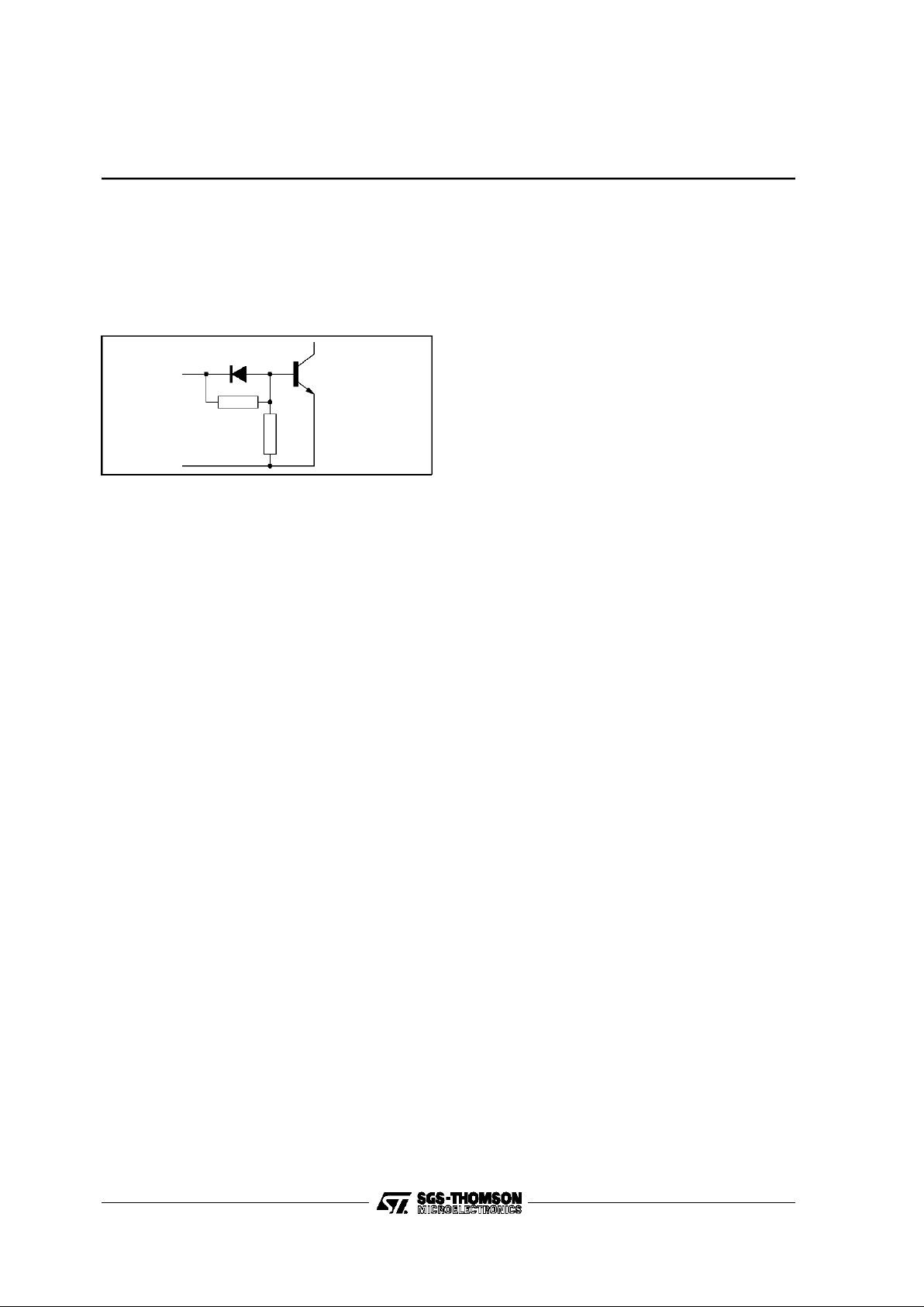
For a proper working,this stage is to be loaded by
the followingcircuit(Figure 1).
II.1.1.5 - VerticalDeflectionStage
This isthe typical applicationofthe TDA8172 used
with a symetrical power supply ±12V in order to
avoid usinga highvalueelectrolytic capacitor.
This stage is designed for driving a yoke with the
following characteristics :
-L≈ 5mH
-R≈8Ω
II.1.1.6 - B+Converter
The B+ is generated by a booststep up converter
working incurrent mode.
The powerMOS Q6startsto conduct at thebeginning of the line sawtooth and it stops when the
voltageon R61(imageof draincurrentof the MOS)
becomes greater than the output voltage of the
error amplifier(inside the TDA9103). This voltage
is setby the regulation loop.
The board offers two possibilites for choosing the
regulationloop :
- Localregulation of B+: SW2 in position1.
- EHTregulation : SW2 in position 2 and feedback
input on J25.
This secondmodewillbe choosen when the board
is connectedon a multi-frequencymonitor.
The main featuresof this converterare the following :
- Frequencyrange 31kHz- 64kHz
- Outputvoltage 70V - 140V
- Input voltage 45V ±X%
- Outputpower 35Wmax.
Youwill find in annexe A the specifications of the
inductanceT2 used in this converter.
BYW98-100
1
Ω
47Ω
BUH715
9103-62.EPS
Figure1
II.1.1.7 - OtherFunctions
X ray protectionTP2
A level higher than 1.6V (TTL level) in this point
inhibitsall theoutputs (Horizontal,Vertical, SMPS,
Blanking).
Blankingoutput TP6
This output is activated in case of Xray detection,
loss of line synchro, power failure (V
CC
, ...) or
activationof theON/OFF switch.
ON/OFFswitch
When the voltage on pin 2 is smallerthan 1V,the
HOUT,VOUT and SMPSoutputsare disabledand
the BLANKoutput TP6is activated.
CS switchJ17
Theses4 outputsaresequentiallyswitchedon(low
level)if the inputhorizontal frequencygoesthrough
the following thresholds : 34kHz, 41kHz, 51kHz,
61kHz.
These frequencies are given for a free running
frequencyequal to 27kHz.
The CS switchoutputs could be used to switchthe
S correctioncapacitors if necessary.
Frame Blanking TP11
This output is in fact the flyback generator of the
vertical booster TDA8172. It could be used for
blankingthe videosignalduring the frame retrace.
II.1.1.8 - Operationwith CompositeSync
When using these standards, the board is not
driven directlyby the sync signals but by a circuit
(microproc or something else) who generatesthe
Hsyncand Vsync signals.Unfortunately,theHsync
signalpresentgenerallya jumpof phaseduringthe
Vsync time. This phase jump disturb the line PLL
anditcantakealongtimetorecovertherightphase
at theend of the vertical sync.
So,wehavetoinhibitthelinePLLduringthevertical
returntime (and a littlelater).
Thisis doneby thediode D4and the time constant
R80-C48.WhenVsyncisatHIGH level,the voltage
on pin 35 is highand the linePLLis inhibited.
The consequenceis that the board will not work
with standardshaving an inverted polarity vertical
synchro. In this case, D4 must be removed or
Vsync must be inverted in order to have a correct
workingof the line PLL.
TDA9103 USER’S MANUAL DEMONSTRATION BOARD
2/10
Page 3
II.1.2 - ControlBoard
This board, required by the first and quick evaluation, is intended to be separated from the main
board forthe connectionto a monitor whenwe will
use thecommand from the microprocessor.
On this board, we find 11 potentiometers for the
generationof thecontrolvoltagesin therange0-5V
(use ofan externalpowersupply).
In addition, thanks to a small circuit with a
monostablegeneratingapseudohorizontalflyback
pulse ; the demoboard can be used without connectingit to a monitor.
ThewidthandthedelayofthepseudoHflybackcan
be adjustedby the trimmers P1 and P2.
II.2 - Instructionsfor Use
II.2.1 - StandAlone Mode
This demoboardis able to work aloneby using :
- The analogcommand fromthe control board,
- Apseudo Hflyback from the controlboard,
- AlocalB+ regulation.
The value of B+ is preset to 100V. This value can
be be changedby changingthe divider R65-R66.
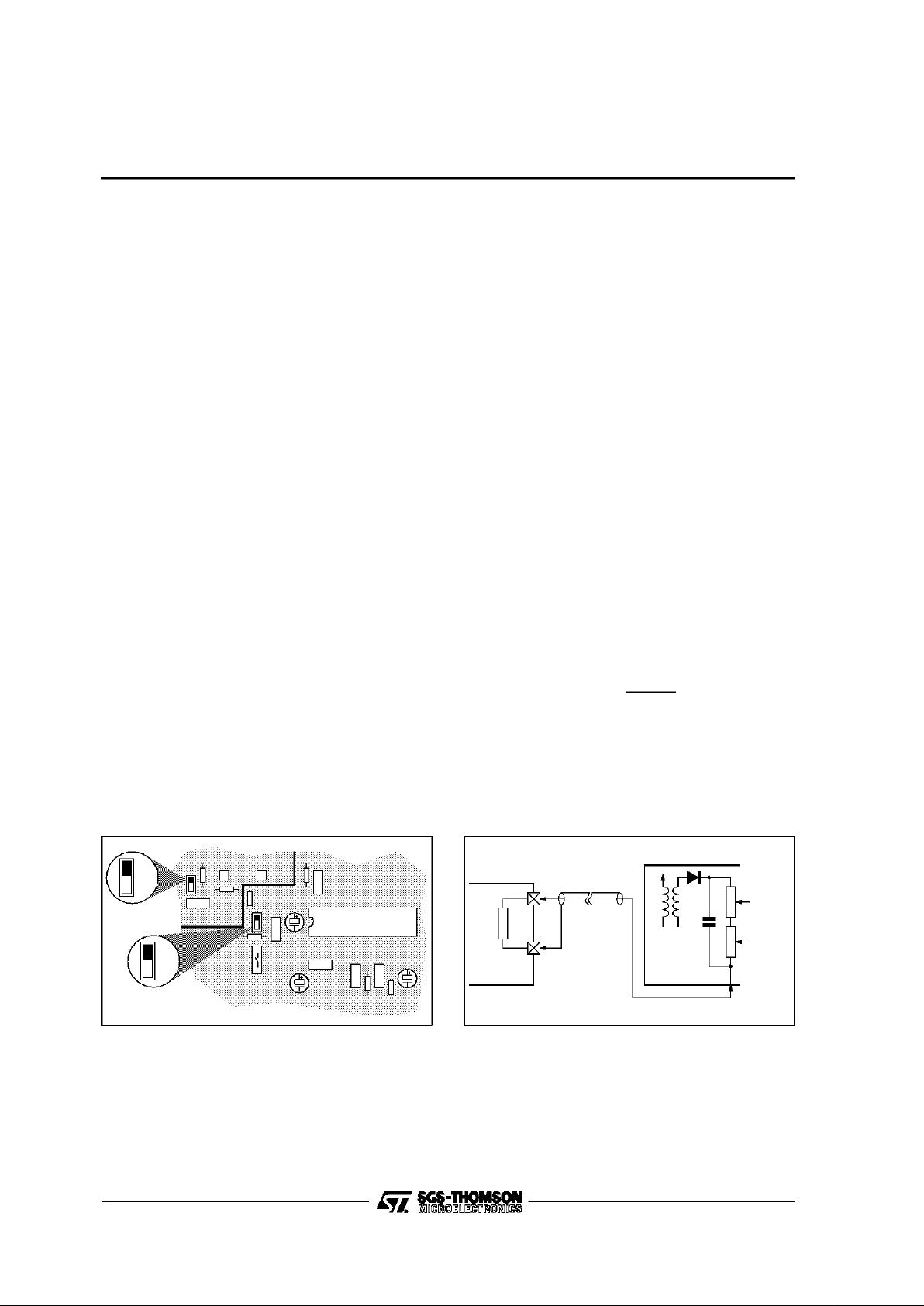
- Configure the two jumper as following (see Figure 2) :
• SW1 position1,
• SW2 position1.
- Connectthe following power supply:
• +12V betweenJ3 and J19,
• -12V between J21 and J19,
• +5V betweenJC4 and JC26,
• 45V 2Abetween J12 and J20,
• 24V between J24 and J20 (these power sup-
pliesare onlyrequiredforSMPS,LINEDRIVER
and EW amplifiertesting).
- Connect the following loads on all the outputs
(Figure4).
- ConnectHsync and Vsyncfrom the pattern generator on J2 and J5 respectively.
II.2.2 - Connectionto aMonitor Chassis
II.2.2.1- AnalogCommand andB+ Regulation
ConfigureSW1in position2and connecttheboard
to thechassis(see Figure5).
II.2.2.2- AnalogCommand andEHT Regulation
ConfigureSW2 in position 2, connecttheboard as
before and connect the HVFEED inputs with a
shieldedcable (see Figure3).
Thevalue ofR79issuitableforgetting25kVapprox
high voltage value with a standard EHT transformer.
When the EHV regulation loop is acting correctly,
the voltage at J25 is ≈5V (depending on the B+
adjust (pin 39) voltage.It’s easy to calculate the
valueof R79 if theequivalentresistanceReq of the
bleederis differentof theone used to develop this
demoboard:
R79 ≈
5 ⋅ Req
EHV
II.2.2.3 - Commands from Microprocessor
Breakoff the control boardand connecttheappro-
priateoutputs of themicro on theconnectorsJ1B,
J2Band J3B.
C35
C45
S1
R71
R67 R73
C36
C33
C2
R32
C9
R31
C34
IC1
R26
R68
TP8
TP9
R72
SW1
SW2
C1
SW2
1
2
SW1
1
2
9103-63.EPS
Figure2
FOCUS
SCREEN
EHT
TRANSFORMER
J25
TP10
R79
75k
Ω
DEMOBOARD
9103-66.EPS
Figure3
TDA9103 USER’S MANUAL DEMONSTRATION BOARD
3/10
Page 4

TDA9103
BYW98-100
1
Ω
47
Ω
12kΩ
10W
The load on B+
is mandatory.
Otherwise the board
could be destroyed.
100
Ω
3W
8
Ω
5mH
9103-64.EPS
Figure4
TDA9103 USER’S MANUAL DEMONSTRATION BOARD
4/10
Page 5

TDA9103
VSYNC
HSYNC
BASE
DRIVE
GND
To LINE FINAL STAGE
HFLY
B+
SMPS
TRANSFORMER
+12V
GND
-12V
VM
GND
V YOKE
To DIODE MODULATOR
+24V
MONITOR CHASSIS
9103-65.EPS
Figure5
P3
47kΩP447kΩP547kΩP647kΩP747kΩP847kΩP947kΩ
P10
47kΩ
P11
47kΩ
P12
47kΩ
P13
47kΩ
+
C4
10µF
+5V
1 J4
1 J26
CON1
SCOR
CCOR
HSIZE
VSIZE
VSHIFT
PINCSH
KEYST
1234567J3
BPLUS
1234J2
FHMIN
HSHIFT
HDF
1234J1
HOUT HFLY
-T+TCXRC
5412
R3
Q
7
Q
6
IC1a
14528
-T
+T
CX
RC
11
12
15
14
R
13
Q9
Q10
IC1b
14528
+12V
C2
100pF
P2 47kΩ
C5
100nF
+
C3
10µF
+12V
+12V
C1 100pF
P1
47kΩ
9103-67.EPS
Figure6
TDA9103 USER’S MANUAL DEMONSTRATION BOARD
5/10
Page 6

+
PINCSH
VSHIFT
SCOR
VSIZE
KEYST CCOR
HSIZE
J3b
H
REF V
REF
HDF
HSHIFT
BPLUS
FHMIN
J2b
IC1
+
+
+
+
+
+
+
V
REF
+12V
TP8
TP9
offon
S1
++
H
REF
+
+
+
TP3
TP7
TP4
+12V
+
0/5V to 2/6V INTERFACE
HDRIVE
J22
T1
G 5576-01
+
VP
R44 10Ω
+12V
HORIZONTAL
DRIVER
STAGE
1
J23
CON2
VYOKE
1
-12V
J21
R36 12kΩ
R70 12kΩ
-12V
+
R36 5.6kΩ
+12V
TP11
+
1
7
2
6
3
5
4
VERTICAL
DEFLECTION
STAGE
J24
E/W
VP
+12V
+
R75
E/W POWER STAGE
1
J25
VP
1
J11
EHT FEEDBACK
+
B+
D3 BYT 13-800
+
+12V
+
VM
T2
G 5446-00
1
J20
1
J12
R72 1kΩ
B+ CONVERTER
+
123456789
10
1617181920
26
27
28
29
30
36
37
38
39
40
1112131415
21 22
23
24
25
31
32
33
34
35
42
41
T
D
A
910
3
2
3
123
123
12341234 567
C24
220pF
400V
C25
22µF
250V
C33
100pF
C46
C47
10nF
10nF
Q5
BC557
Q7
BC547
Q8
BC547
Q3 Q4
BC547
BC547
Q9
TIP122
C10
100nF
C11
470pF
C14
470µF
C11
470pF
C15
220nF
C32
100nF
C12
100µF
35V
C13
470µF
Q10
BC547
Q1
BC557
Q2
STD5N20
C20
100µF
C19
1nF
R35
1kΩ
R45
22kΩ
R46
560Ω
R47a
47Ω 3W
R47b
33Ω
3W
R37
5.6kΩ
D1
1N4004
R41
1.5Ω
R39
220Ω
1/2W
R40
1Ω
1/2W
R49
1.5kΩ
3.3kΩ
R76 R52
10kΩ 10kΩ
R48 R77 R50
10kΩ
1kΩ 1kΩ
R51
10kΩ
R54
470Ω
C21
10µF C44
220pF
R57
12kΩ
R58
47kΩ
1/2W
R59
2.2Ω 1W
R53
1kΩ
R55
10kΩ
R56
2.7kΩ
Q6
IR430F
R63 1kΩ
R62 1kΩ
C22
100µF
C23
220µF 63V
R64
3.3kΩ
R66
1.5kΩ
R65
33kΩ
R79
75kΩ
R61
33Ω
1W
R60
1kΩ
R78 22kΩ
C9
100nF
C8
100µF
R33
10kΩ
C28
47µF
R69
3.9kΩ
TP1
C5
150nF
470nF
C481nF
R80 2.7kΩ
D4
1N4148
C42 1µF
C43 1µF
C27
100nF
C4
C40 1µF
C41 1µF
C37 1µF
C38 1µF
R67 22kΩ
R68 1MΩ
C29 470pF
C6
220nF
C7
4.7µF
R31 1.8kΩ
R32 7.5kΩ
680pF 5%
C2
C3
10nF
C45
220pF
C1
22nF
C39
1µF
C35
1µF
C34
1µF
C36
1µF
C30
C29
100nF
47µF
R71
10kΩ
R2 120kΩ
R5 120kΩ
R8 120kΩ
R3 10kΩ
R6 10kΩ
R9 10kΩ
R12 10kΩ
R15 10k
Ω
R18 10kΩ
R21 10kΩ
R24 10kΩ
R27 10kΩ
R30 10kΩ
R11 120kΩ
R14 120kΩ
R17 120kΩ
R20 120kΩ
R23 120kΩ
R26 120kΩ
R29 120kΩ
R22 3.9kΩ
R19 3.9kΩ
R25 3.9kΩ
R28 3.9kΩ
R16 3.9kΩ
R13 3.9kΩ
R10 3.9kΩ
R7 3.9kΩ
R4 3.9kΩ
R1 3.9k
Ω
9103-53.EPS
Figure7
TDA9103 USER’S MANUAL DEMONSTRATION BOARD
6/10
Page 7

9103-60.TIF
Figure8
TDA9103 USER’S MANUAL DEMONSTRATION BOARD
7/10
Page 8

TDA9103
9103-61.EPS
Figure9
TDA9103 USER’S MANUAL DEMONSTRATION BOARD
8/10
Page 9

III - GUIDELINES FOR LAYOUT AND WIRING
SGS-THOMSON realized a demonstration board
for TDA9103scanning processor. Since this demonstrationboardis expectedtoworkproperlywhile
connected to an existing monitor set with flying
wires,specialattentionmustbe paidtothepossible
misfunctionsthat may be caused by the wiring.
As theprecautionswetook maybeveryuseful also
in normal layouting,we listedthem herebelow,togetherwith otherpieces of advice.
III.1 - GeneralStatement on GroundConnection
ThegroundconnectiontoTDA9103notonlycarries
the supplycurrent,butis also the voltagereference
for various functions. Consequently, it should not
carryhighcurrentswith fasttransients,like:
- Verticalscanning supply
- Supplyfor B+converter
Which would introduce parasitic series voltages
(resistiveand inductive).
Thiswasmadeeasierbycompletelyseparatingthe
powersourcesforverticalandB+.Inside achassis,
thiswouldnecessitateseparatedgroundpinsinthe
SMPStransformer for ±12V(Vertical) and 45..60V
(B+).
III.2 - VerticalSection
III.2.1 - BoosterPart
The +12V and -12V supplies feed the booster in
first ; this way, since the ground point was kept
separated, the high currents implied in vertical
scanning will keep localisedbetween thesupplies
and the booster.
Othertraditionalprecautionsfortheboosterinclude
:
- FilmcapacitorsC31 andC32 with low HFimpedance, near to the booster with short tracks (an
alternatesolutionis toconnect C32 betweenpins
2 and 4) ;
- ”Boucherot cell” R41, C19, near to the booster
withshort tracks ;
- The ground track to driver stage (TDA9103) is
connectedto the footof R40.
III.2.2 - TDA9103 Oscillator and DriverStage
The verticalsectionhas adedicatedreferencevoltage (pin 26)which shouldbefilteredversus vertical
ground (pin 24). Pin 24 may be tied to pin 19
(General ground). All elements relative to Vertical
should be referedto Verticalground (C4,C5, C40,
C41,C42, C43).
The oscillatorcapacitorC4 claims for specialattention. Thevertical sawtoothis obtainedby charging
it at lowrate,thendischargingabruptly.Theswitching from ”discharge” to ”charge”is triggeredwhen
reaching a low threshold.The loop constituted by
C4 and itsconnectingtracks may giverise to parasitic series voltage spikes if there is a switching
circuitat short distance (likethe DC/DC converter
for B+) ; one such spike could randomly trigger
earlyswitchingto”charge”, and theeffectwouldbe
a vertical vibration of the display.Such vibrations
usually occur for determined settings of the horizontal phase.To avoid this, the loop including C4
must haveminimal area, and all switching circuits
(SMPS, DC/DC converter, horizontal scanning)
shouldbe kept remote.
III.3- HorizontalSection
III.3.1 - OscillatorStage
Like Vertical section, Horizontal section has dedicatedvoltagereference(pin5)and Ground(pin4).
Inorderto maintainthe horizontaljittertothelowest
possible value, pin 4 should be kept NOT CONNECTEDTO ANY OTHER GROUND (an internal
connectionalreadyexists withpins19and 24),and
pin 5 should be filtered versus pin 4. This mainly
concerns pins 1, 2, 3, 5, 10, 11, 12, 14, 15, 17.
Moreover,the componentsnotrelatedtohorizontal
shouldnot be connected to pin 4.
As for Vertical section, the capacitors with their
connectingtracksshouldnotconstitutelargeloops,
proneto catchparasitic spikes.
When the various DC inputs are controlled by a
PWM type DAC, the DAC filtering capacitor must
not be refered to pin 4, where it would produce
parasitic voltages, but to the microprocessor
ground ; furthermore, since there is some ripple
between these two grounds, a second filter cell is
needed,with its capacitor connected to pin 4.The
secondfilter resistors are not presenton the demonstrationboard.
III.3.2 - Output Stage
Usually, the horizontal scanning stage is remote
fromthe TDA9103 and the control signal hasto be
transmittedat a distance.
Whenthesignal istakenfrompin 21,pin20should
be connectedtoGND,butnotnecessarilyto pin 19
or nearto theIC.
In the typical application implemented on present
board, the gate capacitance of Q2 will be charged
and dischargedat quite high current for every fast
transitionofpin 21. Thecurrent pathis asfollows :
- For Charge : +12V (thefilteringcapacitor) > Q10
> R44 > gate of Q2 > source of Q2 > minus of
filteringcapacitor
- For Discharge : gate of Q2 > Q1 > source of Q2
TDA9103 USER’S MANUAL DEMONSTRATION BOARD
9/10
Page 10

If these loops have too great area, they will send
disturbingspikestoother circuitrybymutualinductance.For thatreason the best place fortransistors
Q1 and Q10 is : near to the horizontal scanning
transistor. This, of course, could not be implemented on presentboard,which doesnot incorporate thescanningstage.
The driver stage supply voltage, present on C20,
must bewell filtered,since a rippleat thispoint will
induce variations of the power transistor desaturation time,which will causejitter.
When the TDA9103 is controlledOFF,for instance
by X-ray protection, Q2 will remain conductive,
which causes high dissipation in R47.This may be
solved if AC coupling is used between pin 21 and
driverstageQ1-Q10.Thiswasnot implementedon
present board.
III.4 - DC/DC Converter Section
III.4.1 - Keepingthe InformationClean
The converter section receives two informations
from otherparts of the chassis :
- A determined fraction of the voltage to be regulated, which it will manage to keep equal to its
internalreference(5V),
- The voltageon the sense resistorR61, which is
alwayslower than 1.2V.
The internal references for comparison are connected to the localground (pin19) ; consequently,
any voltage difference in the ground track could
influencethe regulatedvoltage and the peak currentin Q6. To avoid this :
- The foot of the divider, R79 + C47, must be
grounded near to the IC (pin 19) ; if this voltage
comes from a transformer,itis betterto carry the
informationto the IC withtwo dedicatedtracks,
- Theground trackbetweenR61 andIC must carry
low-valueor DCcurrents,asexplainedin the first
paragraph.
III.4.2 - AvoidingDisturbingSpikes
WhenQ6 switchesfromONto OFF, thepathof the
currentchanges abruptlyfrom Q6-R61to D3-C25,
and this may give rise to parasitic voltages, by
mutual inductance, in all surrounding circuits
(pleaserefer to the comments about C4 in Vertical
section).This effect will be minimizedif both paths
Q6-R61and D3-C25 are very near toeach other;
in other terms, if the loop Q6-R61-C25-R3 has a
small area.
The driverstage for Q6 is similar tothe one for Q2
and the highsurge currents in itsgate may cause
parasiticspikes in the same way.
III.5- Pincushion(E/W) Section
All the comments relative to DAC control of the
horizontalDC inputsalsoapplyto theE/W section.
Information furnishedis believed to be accurate and reliable.However, SGS-THOMSON Microelectronicsassumes noresponsibility
for the consequences of use of such information nor for any infringement of patentsor other rights of third parties which may result
from its use. No licence isgranted by implication or otherwise under anypatent or patent rights of SGS-THOMSON Microelectronics.
Specifications mentioned in this publication are subject to change without notice. This publication supersedes and replaces all
information previouslysupplied. SGS-THOMSON Microelectronics products are not authorized foruse as critical components in life
support devicesor systems without express writtenapproval of SGS-THOMSON Microelectronics.
1995 SGS-THOMSON Microelectronics - All Rights Reserved
Purchase of I
2
C Components of SGS-THOMSON Microelectronics, conveys a license under the Philips
I
2
C Patent. Rights to use these components in a I2C system, is granted provided that the system conforms to
the I
2
C Standard Specificationsas defined by Philips.
SGS-THOMSON Microelectronics GROUP OF COMPANIES
Australia - Brazil - China - France -Germany - Hong Kong - Italy -Japan - Korea - Malaysia - Malta - Morocco
The Netherlands - Singapore -Spain - Sweden - Switzerland - Taiwan - Thailand - United Kingdom - U.S.A.
TDA9103 USER’S MANUAL DEMONSTRATION BOARD
10/10
 Loading...