

HORIZO NTAL SECTION
.
SYNCHRONIZATION INPUT : TTL COMPATIBLE, NEGA TIVE EDGE TRIGGERED
.
SYNCHRONIZATION INDEPENDENT FROM
DUTY CYCLE TIME
.
OSCILLATOR : FREQUENCY RANGE FROM
15kHz to 100kHz
.
HORIZONTAL OUTPUT PULSE SHAPER
AND SHIFTER
.
PHASE COMPARATOR BETWEEN SYNCHRO AND OSC ILLAT OR ( PLL1)
.
PHASE C OMPARATOR BETWEEN FLYBACK
AND OSCILLATOR (PLL2)
.
INTERNAL VOLTAGE REGULAT O R
.
DC COMPATIBLE CONTROLS FOR PHASE
AND FREQUENCY
.HORIZONT AL OUTP UT DUTY CYCLE : 48%
TDA9102F
H/V PROCESSOR FOR TTL V.D.U
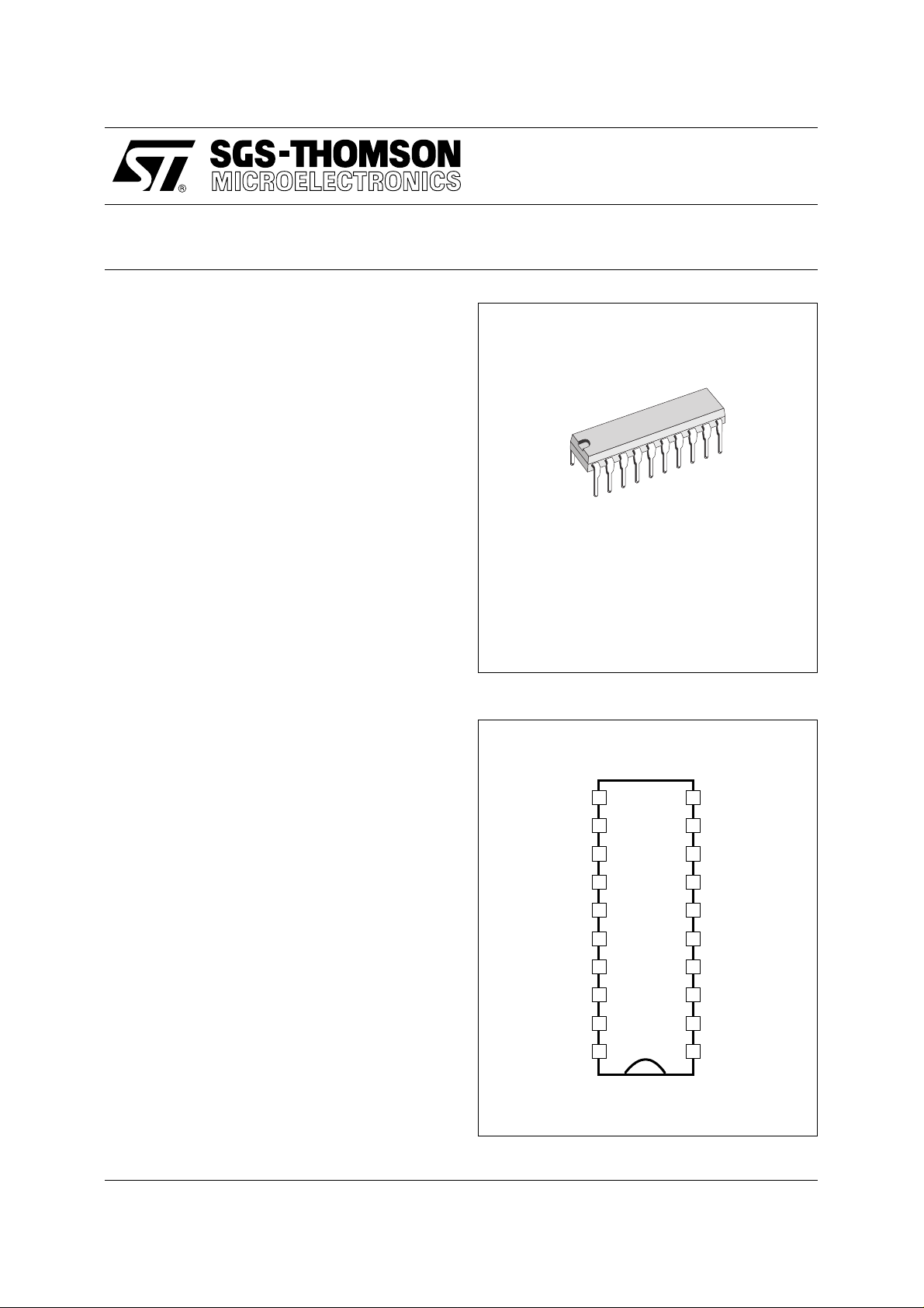
POWERDIP20 (0.4)
(Plastic package)
ORDER CODES : TDA9102F
VERTICAL SECTION
.
SYNCHRONIZATION INPUT : TTL COMPATIBLE, NEGA TIVE EDGE TRIGGERED
.
SYNCHRONIZATION INDEPENDENT FROM
DUTY CYCLE TIME
.
OSCILLATOR : FREQUENCY RANGE FROM
30Hz to 120Hz
.
RAMP GENERATOR WITH VARIABLE GAIN
STAGE
.
VERTICAL RAMP VOLTAGE REFERENCE
.
INTERNAL VOLTAGE REGULAT O R
.
DC COMPATIBLE CONTROLS FOR FREQUENCY, AMPLITUDE AND LINEARITY
DESCRIPTIO N
The TDA9102F is a monolit hic integrated c ircuit for
horizontal and vertical sync processing in monochrome and color video displays driven by input
TTL compatible signals.
The TDA9102F is supplied in a 20 pin dual in line
package with pin 1 1 connected to ground and used
for heatsinking.
PIN CONNECTIONS
Substrate Ground
Vertical Frequency Preset
Vertical TTL Input
Vertical Ramp Output
Vertical Amplitude Adjust
Vertical Linearity Adjust
Linearity Output
Vertical Reference Voltage
C13
11
12
13
14
15
16
17
18
19
V
20
S
Horizontal Phase Adjust
10
Phase Comparator 2 Output
9
Horizontal Flyback Input
8
Horizontal Output
7
Horizontal Power Ground
6
C5
5
Horizontal TTL Input
4
Phase Comparator 1 Output
3
C2
2
R1
1
9102F-01.EPS
May 1994
1/7
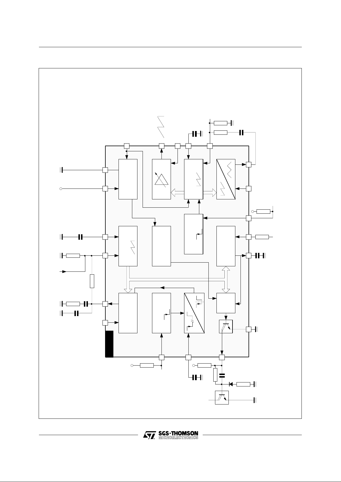
TDA9102F
BLOCK DIAGRAM
DC FREQUE NCY
PRESET
R12
C13
REF
V
19
DC VERTICAL
AMPLITUDE
ADJUSTEMENT
16
13
R18
12
C18
VOLTAGE
OSCILLATOR
HORIZONTAL
PHASE
COMPARATOR
REGULATOR
VOLTAGE
LOW SUPPLY
PROTECTION
1
ϕ
HORIZONTAL
TTL INTERFACE
4 15
S
V
C2
R1
R2
DC FRE QUENCY
ADJUSTEMENT
R3
C3
C1
DC HORIZONTAL
PHASE
ADJUSTEMENT
10 3 1 2 1120
TDA9102F
VERTICAL
OSCILLATOR
VERTICAL
TTL IN T ER FACE
5
S
V
2
ϕ
PHASE
COMPARATOR
HOR.
PULSE
SHAPER
7
DC VERTICAL
LINEARITY
ADJUSTEMENT
R14
+ 5V
R8
C9
6981417 18
VERTICAL
HORIZONTAL
SYNC.
FLYBACK
INPUT
INPUT
+ 5V
R4
2/7
HORIZONTAL
SYNC.
INPUT
C5
9102F-02.EPS
TDA9102F
ABSOLUTE MAXIMUM RATINGS
Symbol Parameter Value Unit
V
V
SYNC
I
I
I
P
T
stg
THERMAL D ATA
Symbol Parameter Value Unit
R
th(j-c)
R
th(j-a)
ELECTRICAL CHARACT E RIS TICS
(T
amb
Symbol Parameter Test conditions Min. Typ. Max. Unit
HORIZONTAL SECTION
V
V
V
K
V
3
I
K
V
T
V
V
7
I
FLY
V
I
Supply Voltage 18 V
S
OH
15
19
Sync Input Peak Voltage + V
Output Sinking Peak Current (Pin 7 ; t < 3µs) 2 A
Output Current (Pin 15) - 10 mA
Output Current (Pin 19) - 10 mA
Total power dissipation
tot
● T
● T
amb
< 90oC
pin
< 70oC
S
1.4
1.5
, TjStorage and Junction Temperature - 40 to 150
Junction-case Thermal Resistance 40
Junction-ambient Thermal Resistance 55
= 25oC, VS = 12V, refer to the test circ uits, unles s otherwise sp ecified)
Supply Voltage Range 10.5 12 15.5 V
S
I
Supply Current 40 70 mA
S
Voltage Reference at Pin 1 I1 = 0.5mA 3.2 3.5 3.8 V
1
Current at Pin 1 - 1 mA
I
1
Voltage Swing at Pin 2 3.7 4 4.3 V
2
Free Running Frequency Constant fo = 1/(K0 x R1 x C2) 3.7 4 4.3
0
- V1 Control Voltage Range (See technical note 1) 1.6 2.5 V
Peak Control Current 3 mA
3
Gain Phase Comparator φ1
3
K3 = 2 x I3 / 360
Sync Threshold Input (neg. edge) ● Sync high
4
Current at Pin 4 ● Input high
I
4
Input Pulse Duration T = 1/f
4
Monostable Threshold 5.6 6 6.4 V
5
Internal Pulse Width (t5 = C5 x V5 /I5) C5 = 220 pF
t
5
t
Output Pulse Duration (low) - T = 1/f
7
H
H
● Sync low
● Input low - 10
@ fH = 27.64kHz 1 0.9T µs
(see technical note 2)
fH = 27kHz
fH = 70kHz
0.44T
0.41T
sat Output Saturation Voltage I7 = 600 mA 1.2 2.5 V
t
Permissible delay between output pulse
D
leading edge and flyback pulse leading edge
(for keeping a constant duty cycle) ; T =
See technical note 4
@ fH = 27kHz
1
f
H
Flyback Input Current at Pin 8 ● Flyback On
● Flyback Off
Clamp voltage at Pin 8 ● I
8
I
Current for switching low the output pulse 0.7 2 mA
8
Peak control current 0.9 mA
9
● I
8 =
8
1mA
= - 1mA
17
28
0.8
10 µA
3.6 µs
0.48T
0.52T
0.45T
0.49Tµsµs
0.48 T - t
0.7
FLY
2mA
-1
0.6
- 0.6
V
W
W
o
C
o
C/W
o
C/W
PP
µA
degree
V
V
µA
s
mA
V
V
9102F-01.TBL
9102F-02.TBL
9102F-03.TBL
3/7

TDA9102F
ELECTRICAL CHARACTERISTICS (continued)
(T
= 25oC, VS = 12V, refer to the test circuits, unless otherwise specified)
amb
Symbol Parameter Test conditions Min. Typ. Max. Unit
HORIZONTAL SECTION
Phase sensitivity at Pin 9 (See technical note 3) 67.5
K
9
V
Control voltage range 0.5 4.5 V
10
K
Phase control sensitivity at Pin 10 23 26 29
10
HADJ Horizontal phase adjustment for V10 varying
from 0.5 to 4.5V (27.64kHz)
Zero degree phase: flyback
centered on the middle of the
- 45 + 45 degree
pulse at Pin 5
K
Phase jitter constant (jitter =
K
1
K
Frequency drift versus supply voltage
2
K
=
2
dF
dV . f
. 10
6
H
1
106 . f
)
H
100 150 ppm
VS = 10.5V to 15.5V 400 ppm
VERTICAL SECTION
Voltage reference at Pin 12 3.2 3.5 3.8 V
V
12
I
13
Current gain at Pin 13
I
12
Typical Vertical Sawtooth Amplitude
V
13
(Pin 13) for Center Frequency
t
II
I
Discharge time at Pin 13 C18 = 0.22 µF, V13 = 4V
FALL
f
Maximum Vertical Frequency Vertical Sync Low
VL
f
Minimum Vertical Frequency Vertical Sync High
VH
K
Synchro window constant ts =
K
14
V
Sync input threshold (negative edge) ● Sync high
14
Current at Pin 14 ● Input high
I
14
Input pulse duration T =
t
14
V
Average value of voltage on Pin 15 V13 = 4VPP, V16 = 2.5V 4 V
15
I Output current at Pin 15 1 mA
15
Buffer gain constant at Pin 15
K
15
K
16
I
16
I
17
V
18
K
18
V
19
Current at Pin 19 2mA
19
= K15 . V
V
15PP
13PP
Buffer variable gain constant at Pin 15 :
∆V
K
=
16
15PP
∆V16 . V
13PP
Input bias current at Pin 16 V16 = 0.5V - 50 µA
Input bias current at Pin 17 V17 = 4.5V 50 µA
Average voltage at Pin 18 : V18 = 2 +
Linearity correction constant : K18 =
Voltage reference at Pin 19 (See technical note 5) 7.6 8 8.4 V
14
f
V
1
f
V
V
∆V
∆V
I12 = 100µA
(I12 max. = 200µA)
To be adjusted by I
12
PP
0.94 1 1.06
4V
10 22 µs
84 Hz
C
= 220nF, R
Pin 13
Pin 12
= 58kΩ
56 Hz
C
= 220nF, R
Pin 13
Pin 12
= 58kΩ
(See technical note 6) 0.333
28
● Sync Low
● Input Low V
= 0.8V - 10
14
@ fV = 64.75Hz 10 0.5T µs
V16 = 2.5V 0.95
2.5V < V16 < 4.5V
0.5V < V
18PP
V17 = 3.5V, R18 not connected 3 V
2
18PP
V
17
13PP
< 2.5V
16
= 4V,1.5V < V17 < 4.5V 1
0.1
0.1
degree
degree
0.8
10 µA
µA
V
V
V
V
V
PP
V
V
-1
-1
9102F-04.TBL
4/7

TDA9102F
ELECTRICAL CHARACTERISTICS (continued)
(T
= 25oC, VS = 12V, refer to the test circuits, unless otherwise specified)
amb
Symbol Parameter Test conditions Min. Typ. Max. Unit
VERTICAL SECTION
6
dF .
K
Frequency drift versus supply voltage K17 =
17
10
dV . f
VS = 10.5V to 15.5V 300
V
ppm
V
9102F-05.TBL
Technical note 1
C2
f
H (nom)
HORIZONTAL
OSCILLATOR
12
R1
I1
= 26.8 kHz
R2
V
3H
V
3L
3
if
C1
R3
C3
HOR. SYNC.ϕ1
V3HV
V
3L
DC
V
DC
R1 = 6.8k Ω
R2 = 56 kΩ
C2 = 1.8 nF
f
pull-in
= f
H (nom)
V
3
V
/ R1
1
= f
H (nom)
I
f
(A)
I
o
− V1 / R2
where: V1 = 3.5V and V3 - V1 is the control
voltage range.
The voltage at Pin 3 is limited by two clamping
diodes at the voltage V
and V
3H
3L
When the PLL1 is synchronized and perfectly
tuned, V
= V1.
3
Technical note 3
K
= 67.5 degrees/volt represents the slope of the
9
oscillator charging period of the waveform at
Pin 2:
K
=
9
360 x 0.75
4
degree
V
Technical note 4
The second PLL can recover the storage of horizontal output stage maintaining a constant duty
cycle till the trailing edge of the output pulse gets
the trailing edge of the flyback pulse. From this
point on, only the leading edge of the output pulse
will be shifted covering a total phase shift of: 0.30T ;
overcoming this value, it will produce a notch in the
output pulse (@ f
= 27kHz).
H
Technical note 5
The voltage reference at Pin 19 can be used to
polarize the DC operating point of the vertical
9102F-03.EPS
booster. This v oltage corres p onds to the double of
the mean value voltage of the vertical sawtooth at
Pin 13.
Technical note 6
V (V)
= 6.8VV
H
= 6VV
= 5.2V
V
L
Remark: The value of C2 influences the horizontal
oscillator free running frequency; it doesn’t effect
the relative pull-in range. If the horizontal frequency is changed by using R1, the pull-in range
changes accordingly with the formula (A).
Technical note 2
The internal pulse "t
generator "I
5
", is generated by the current
5
" charging the external capacitor
"C5", according with the formula (B):
=
t
5
C5 . V
I
5
5
(B), t
T
H
=
is recommended.
5
12
V
H
ts =
LL
− V
t
= 2VV
V
L
=
s
(V
− V
H
L)
(VH − VLL)
H
1/f
− V
t (s)
1/fv
ts
9102F-04.EPS
LL
V
K
1
14
=
f
f
V
V
5/7

TDA9102F
APPLICATION DIAGRAM (with TDA8172)
S
V
14V
Hor. Out
F
µ
C11
Vert.
Yoke
Hor. Power GND
Ω
R13
120
2200
Ω
1
Ω
R16
V
O
V
I
GND
18
C20
R15 1.5k
220nF
F
F
µ
C14 10
47kΩ *
F
µ
C15
1
12
13
11
2
3
Ω
R24 56k
1
Ω
R26 22k
22nF
µ
C13
47
Ω
Ω
R18 1.2k
R17 2.7k
"C" Correction
Note : * The value of R19 depends on CRT. On the mock up R19 is substitued
with a resistance + trimmer for ge neric applications.
Ω
R20 150k
P4
Ω
R21
62k
Ω
R22
220k
C16
220nF
C17
1.8nF
C18
15nF
Ω
F
µ
R23
C19
3.3k
2.2
Ω
R25
6.8k
Ω
47k
Ω
5
R14
C12
3
IC3
C9
R11
C8
0.22nF
100nF
Ω
22k
F
µ
100
TDA8 172
TDA9102F
Ω
R27 100k
1.5
41
Ω
R12 10k
R19
15
8
9
F
µ
C10
Ω
R9
2W
82
D1
C7
220
1N4001
F
µ
1000
6
2
7
IC1 7812
C1
100nF
C6
F
µ
C2
470
C5
15nF
Ω
Ω
P3
R7
39k
Ω
P2
R5
39k
Ω
P1
R3
51k
R2
R1
Ω
R8
47k
5.1k
C4
15nF
Ω
Ω
R6
47k
5.1k
C3
15nF
Ω
Ω
R4
22k
47k
Ω
3.3k
Ω
3.3k
Ω
100nF
R10 22k
6
7
20
19
10
IC2
14 17 16
4
5
Ω
R29
2.2k
C21
Ω
R28
2.2k
6/7
Ω
P5
47k
Hor. Sync.
Vert. Sync.
Fly. Input
9102F-05.EPS

PACKA G E MECHANICAL DATA
20 PINS - PLASTIC POWERDIP (0.4)
TDA9102F
I
a1
L
Z
e3
b
B
e
E
Z
D
20 11
F
110
Dimensions
Min. Typ. Max. Min. Typ. Max.
a1 0.51 0.020
B 0.85 1.4 0.033 0.055
b 0.5 0.020
b1 0.38 0.5 0.015 0.020
D 24.8 0.976
E 8.8 0.346
e 2.54 0.100
e3 22.86 0.900
F 7.1 0.280
i 5.1 0.201
L 3.3 0.130
Z 1.27 0.050
Millimeters Inches
b1
PMDIP20W.EPS
DIP20PW.TBL
Information furnished i s believed to be accurate and rel iabl e. However, S GS-THOMSON Microel ectroni cs assumes no responsibil ity
for the consequences of use of such information nor for any infringement of patents or other rights of third parties which may result
from its use. No licence is granted by implication or otherwise under any patent or patent rights of SGS-THOMSON Microelectronics.
Specifications mentioned in this publication are subject to change without notice. This publication supersedes and replaces all
information previously supplied. SGS-THOMSON Microelectronics products are not authorized for use as critical components in life
support devices or systems without express written approval of SGS-THOMSON Microelectronics.
© 1994 SGS-THOMSON Microelectronics - All Rights Reserved
2
Purchase of I
2
C Patent. Rights to use these components in a I2C system, is granted provided that the system conforms to
I
Australia - Brazil - China - France - Germany - Hong Kong - Italy - Japan - Korea - Malaysia - Malta - Morocco
The Netherlands - Singapore - Spain - Sweden - Switzerland - Taiwan - Thailand - United Kingdom - U.S.A.
C Components of SGS-THOMSON Microelectronics, conveys a license under the Philips
2
C Standard Specifications as defined by Philips.
the I
SGS-THOMSON Microelectronics GROUP OF COMPANIES
7/7
 Loading...