

PAL/NTSC DECODER AND VIDEO PROCESSOR
.
RGB OUTPUTS
.
SINGLE CHIP CHROMA AND LUMINANCE
PROCESSOR
.
DC CONTROL BRIGHTNESS, CONTRAST,
SATURATIONANDHUE
.
FEWEXTERNALCOMPONENTS
.
FAST BLANKING INPUT FOR OSD INSERTION
.
SUPERSANDCASTLE INPUT
DESCRIPTION
The TDA8219 is a monolithic integrated color decoder for the PAL/NTSC standard.It includes in a
20 pinsIC all the functions required for theidentificationanddemodulationofPAL/NTSCsignals,and
all the videoprocessor functions up to the drive of
the video stages. Used with TDA8213 (video
& sound IFsystem)andTDA8214B(H/Vdeflection
circuit),thisICpermitsacompletelow-costsolution
for PAL/NTSCapplications.
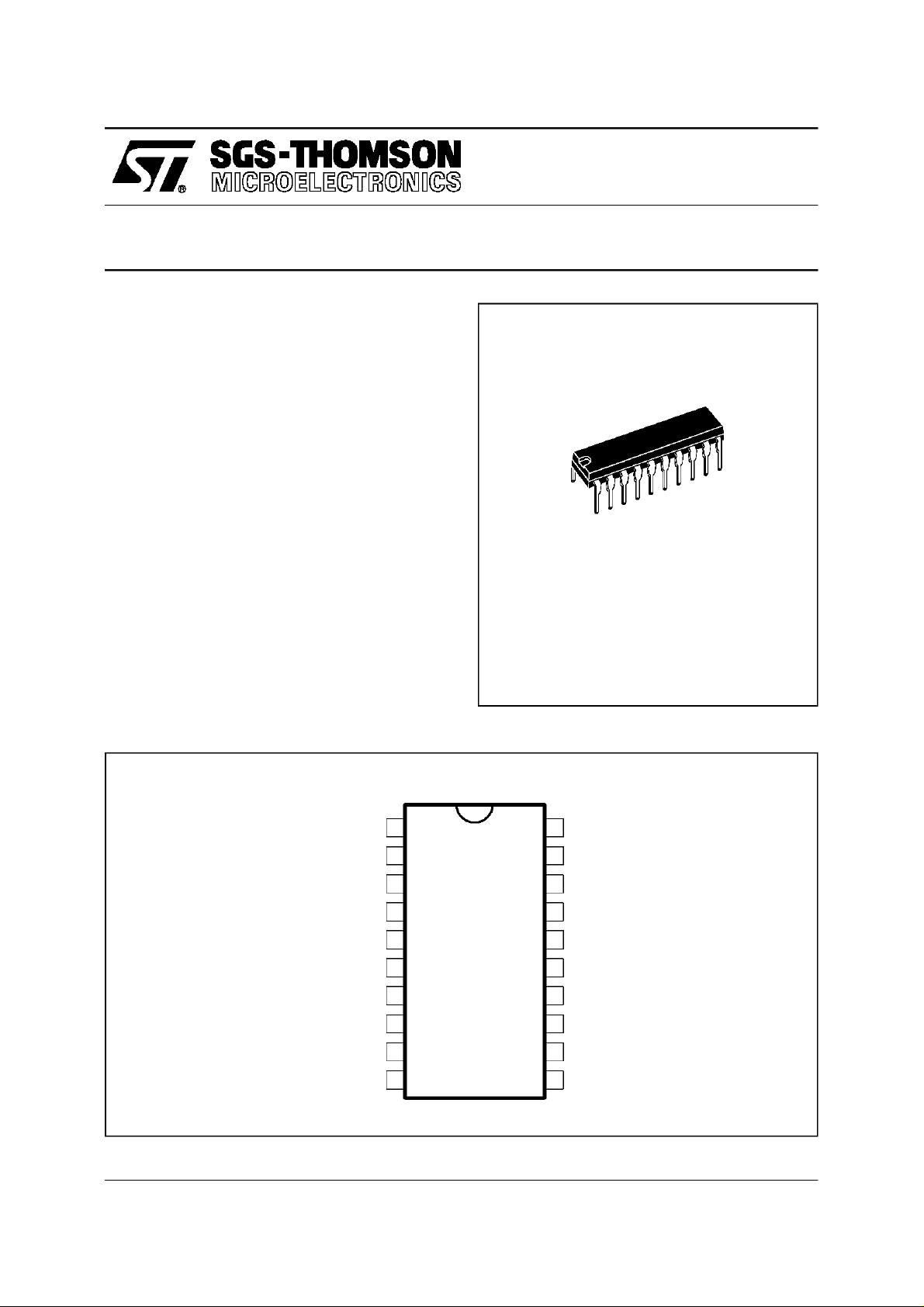
TDA8219
DIP20
(Plastic Package)
ORDER CODE : TDA8219
PIN CONNECTIONS
BRIGHTNESSCONTROL
SUPERSANDCASTLEINPUT/
FASTBLANKING INPUT
CONTRASTCONTROL
DELAYEDCHANNEL INPUT
CHROMINANCE OUTPUT
SATURATIONCONTROL
CHROMINANCE INPUT
April 1996
RGBCLAMP
VIDEOINPUT
HUECONTROL
1
2
3
4
5
6
7
8
9
10
20
19
18
17
16
15
14
13
12
11
V
CC
BLUEOUTPUT
GREENOUTPUT
REDOUTPUT
PLL LOOP FILTERINPUT
PALKILLER
XTAL
NTSCKILLER
ACCCAPACITOR
GROUND
8219-01.EPS
1/9

TDA8219
BLOCK DIAGRAM
XTAL
VCO
LPF
SSC/FB
INPUT
TDA8219
14
16
DETECTOR
FLIP-FLOP
4
HUE
CONTROL LUMA CONTRAST
7
XVCO
P/N
P/N
HUE
SW
PHASE
SSC/FB
INPUT
11 1213 15
90deg
B Gate
GND
KILLER
P/N
OUTPUT
3
VIDEO
INPUT
CONTRAST
CONTROL
PHASE
SHIFTER
90deg
±90DEG
SHIFTER
PAL KILLER
NTSC KILLER
KILLER
CAP
NTSC
5
0deg
±90deg
KOP
Contrast
B-Y
DEMODULATOR
P/N
DL
MATRIX
BURST DETECTOR
BURST DETECTOR
KILLER
CAP
PAL
R-Y
VU
±90deg
±90DEG
0DEG
AGC
CAP
R-Y
G-Y
B-Y
0deg
V
CC
20
RGB OUTMATRIX
BRIGHTNESS
CONTROL
SATURATION
CONTROL
P/N
ACC
10
CHROMA
17
18
19
1
RGB CLAMP
2
6
8
9
Contrast
ROUT
GOUT
BOUT
BRIGHTNESS
DL INPUT
DL OUT
SATURATION
8219-02.EPS
ABSOLUTEMAXIMUM RATINGS
Symbol Parameter Value Unit
T
T
V
CC
OPER
STG
Supplyvoltage 12 V
Operating temperature 0 , + 70
Storage temperature -55 , + 150
THERMALDATA
Symbol Parameter Value Unit
R
TH (j-a)
Junction to ambient thermal resistance Max. 80
o
C/W
DC AND AC ELECTRICALCHARACTERISTICS
=9V,T
V
CC
Symbol Parameter Test Conditions Min. Typ. Max. Unit
V
Supply Voltage 8 9 10 V
CC
I
Supply Current No Load at VCC=9V 20 30 40 mA
CC
P
TotalPower Dissipation No Load 270 450 mW
D
LUMINANCE INPUT (Pin3)
Input Level (Black to White) 350 500 mV
DC Operating Voltage No Input Signal 2.5 2.8 3.1 V
Input Current During Burst Period
2/9
=25oC (unlessotherwisespecified)
AMB
Out of Burst Period
± 50 ± 100 ± 1505µA
o
C
o
C
8219-01.TBL
8219-02.TBL
PP
µA
8219-03.TBL

TDA8219
DC AND AC ELECTRICAL CHARACTERISTICS (continued)
=9V,T
V
CC
Symbol Parameter Test Conditions Min. Typ. Max. Unit
CHROMINANCE INPUT(Pin 10)
Input Level 300 900 mV
ACC Control Range Change of Burst Signal over
Minimum Burst Signal Amplitude within the
ACC Control Range
Input Impedance 6 8 12 kΩ
DC Operating Voltage No Input Signal 2.3 2.8 3.3 V
SSC INPUT (Pin 4)
Burst GateThreshold 7.0 7.5 8.0 V
Line Blanking Threshold 3.1 3.6 3.9 V
Frame Blanking Threshold / Fast Blanking 0.5 1 1.5 V
Input Current 60 µA
CONTRAST CONTROL INPUT (Pin 5) (See Figure 1)
Input Current 10 µA
Contrast Control Range 20 dB
SATURATIONCONTROL INPUT (Pin 9) (See Figure 2)
Input Current 10 µA
Tracking between Luminance and
Chrominance Signals over 10 dB Contrast
Control
BRIGHTNESS CONTROLINPUT (Pin 1) (See Figure 3)
Input Current 10 µA
ACC CAPACITOR (Pin 12)
Charging Current During Burst Gate Period 200 µA
Discharging Current DuringBurst Gate Period 10 µA
Leakage Current Out of Burst Gate Period 5 µA
PALKILLER CAPACITOR (Pin 15)
Color off Voltage No Chroma Signal 5.2 V
Color on Voltage 5.4 V
PALflip-flop inhibition level 3.2 V
Control Current 200 µA
Leakage Current 5 µA
Voltagewith Nominal Input Signal 6.0 V
NTSC KILLER CAPACITOR (Pin 13)
Color off Voltage No Chroma Signal 5.2 V
Color on Voltage 5.4 V
Control Current 200 µA
Leakage Current 5 µA
Voltagewith Nominal Input Signal 6.0 V
PLL LOOP FILTER (Pin 16)
Control Current 800 µA
Leakage Current 5 µA
SUBCARRIER OUTPUT (Pin 8)
Output Burst Amplitude Within ACC Control Range 1.6 2.4 3.0 V
=25oC (unless otherwisespecified)
AMB
whole ACC Control Range < 1dB
30 dB
30 mV
2dB
PP
PP
PP
8219-04.TBL
3/9

TDA8219
DC AND AC ELECTRICALCHARACTERISTICS (continued)
=9V,T
V
CC
Symbol Parameter Test Conditions Min. Typ. Max. Unit
DELAYED CHANNEL INPUT (Pin6)
DC Operating Voltage No Input Signal 2.0 2.2 2.4 V
Input impedance 6 8 12 kΩ
RGB OUTPUTS (Pins 17-18-19)
Output Signal Amplitude
(Black to White)
Blue Channel Output Amplitude
(no Y)
Individual Output Sinking Current 1.5 2 2.5 mA
Maximum Peak White Level 7.4 7.8 8.2 V
Blanking Level 1.0 1.2 1.4 V
Black Level Differential Error 350 mV
Relative Variationin Black Level
with Various Saturation, Contrast
and Brightness Control Level
Black Level Thermal Drift 0.5 mV/
DifferentialBlack Level Drift over
40
Frequency Response(-3dB) 7 MHz
HUE CONTROLINPUT (Pin 7 ) (see Figure 4)
Control Range ± 20 ± 45 deg
Input Current 10 µA
NTSC Select Voltage 2.0 6.0 V
PALSelect Voltage 00 0.5 V
XTAL(Pin 14)
Catching Range PAL, XTAL with CM = 13fF
RGB CLAMP CAPACITOR (Pin 2)
Control Current 50 100 150 µA
Leakage Current 5 µA
Figure 1 : Contrast Control VoltageRange
Gain(%)
100
=25oC (unlessotherwisespecified)
AMB
o
C TemperatureRange
0.35V B to W, Signal @ Pin 3,
Contrast @ 4.2V,Sat. @ 1.6V,
Brig. @ 3.5V
300mV
Burst Amplitude at Pin10,
(B-Y),Signal with 200mV
PP
Contrast @ 4.2V,Sat. @ 4.2V,
Brig. @ 3.5V
NTSC, XTALwith CM = 13fF
Figure2 : SaturationControl VoltageRange
Gain (%)
100
2.80 3.15 3.50 V
3.5 3.9 4.3 V
PP
5mV
± 700
± 700
10 mV
Hz
Hz
PP
o
C
8219-05.TBL
75
50
25
0 123
4/9
Contrast Control
Voltage(V)
4 5
75
50
25
0123
8219-03.EPS
Saturation Control
Voltage (V)
45
8219-04.EPS

TDA8219
Figure 3 : BrightnessControlVoltage Range
Black Level (V) at RGB Outputs
8
6
4
2
Brightness Control Voltage (V)
0 2468
8219-05.EPS
INPUT / OUTPUTPIN CONFIGURATION
Figure 5 : Pins 1 - 2 Configuration
9V
Figure4 : HueControl VoltageRange
+45°
0
HUE Control
-45°
Voltage (V)
012345
Figure6 : Pin3 Configuration
9V
8219-06.EPS
1
Burst
Gated
Figure 7 : Pin 4 Configuration
9V
V
REF
V
REF
2
GREEN
Channel
V
REF
Black Level
Clamping
3V
8219-07.EPS
REF
8219-08.EPS
Figure8 : Pin5 Configuration
9V
5V
REF
4
V
REF
8219-09.EPS
8219-10.EPS
5/9

TDA8219
INPUT / OUTPUTPIN CONFIGURATION (continued)
Figure9 : Pin6 Configuration
V
REF
9V
6
V
REF
Figure11: Pin 8 Configuration
9V
Figure10 : Pin 7 Configuration
7
8219-11.EPS
Figure12 : Pin 9 Configuration
9V
8219-21.EPS
9V
Figure 13 : Pin 10 Configuration
9V
V
REF
10
V
REF
9
V
REF
8
8219-12.EPS
8219-13.EPS
Figure14 : Pin 12 Configuration
9V
9V
9V
12
6/9
8219-14.EPS
8219-15.EPS

INPUT / OUTPUTPIN CONFIGURATION (continued)
TDA8219
Figure15 : Pins 13 - 15 Configuration
9V 9V
Figure 17 : Pin 16 Configuration
Base Current
Compensation
Phase
Comparator
Pins 13-15
16
9V
9V
Figure16 : Pin 14 Configuration
9V
14
8219-16.EPS
Figure18 : Pins 17 - 18 - 19 Configuration
9V
Pins 17
18-19
8219-18.EPS
8219-17.EPS
8219-19.EPS
7/9

TDA8219
APPLICATIONDIAGRAM (with OSD capability)
R2 8kΩ
V
CC
R3
22kΩ
R6 8kΩ
100nF
C4 100nF
FB
V9V
1
2
20
R25 220Ω
19
C22
100nF
CC
C24
470µF
D3
R
D2
G
D1
B
GND
R23
1kΩ
R14 1kΩ
R15
1kΩ
FB
R21
390Ω
330ns
SSC
NTSC
R3 10kΩ
L4
10µH
R35
V
CC
L3
CT1
Q2
R17 39kΩ
R18
22kΩ
R19 12kΩ
DL
V
CC
C6
120pF
R1 39kΩ
R4
22kΩ
R7 12kΩ
PAL
R22
390Ω
L1
10µH
C5 10nF
C11 10nF
Q3
C23
10nF
750Ω
R24
3
4
5
100nF
6
7
100nF
8
T
D
A
8
2
1
9
R26 220Ω
18
R27 220Ω
17
16
15
14
13
R31 18kΩ
C17
4.7nF
C21
100nF
X1 3.58MHz
X2 4.43MHz
C19
100nF
Q4
C18
100nF
Q6
NTSC
PAL
R30 680Ω
R29 680Ω
R28 680Ω
R32 330kΩ
R33
470kΩ
B
G
R
V
CC
8/9
CVBS
R34
75
R3 39kΩ
V
CC C10
R8 12kΩ
R16 1kΩ
CT2
Ω
NTSC
Q1
R5
22kΩ
120pF
C9
9
100nF
10
C8 10nFC7 10nF
L2
µH
10.5
12
C20
100nF
11
8219-20.EPS

PACKAGE MECHANICAL DATA
20 PINS- PLASTICDIP
TDA8219
Dimensions
Min. Typ. Max. Min. Typ. Max.
Millimeters Inches
a1 0.254 0.010
B 1.39 1.65 0.055 0.065
b 0.45 0.018
b1 0.25 0.010
D 25.4 1.000
E 8.5 0.335
e 2.54 0.100
e3 22.86 0.900
F 7.1 0.280
I 3.93 0.155
L 3.3 0.130
Z 1.34 0.053
Information furnished is believed tobe accurate and reliable. However,SGS-THOMSON Microelectronics assumes no responsibility
for the consequences of use of suchinformation nor for any infringement of patents or other rights of third parties which may result
from itsuse. No licence isgranted by implication or otherwiseunder anypatent orpatent rights of SGS-THOMSON Microelectronics.
Specifications mentioned in this publication are subject to change without notice. This publication supersedes and replaces all
information previously supplied. SGS-THOMSON Microelectronics products are not authorized for useas critical componentsin life
support devices or systems withoutexpress written approval of SGS-THOMSON Microelectronics.
1996 SGS-THOMSON Microelectronics - All Rights Reserved
Purchase of I
2
I
C Patent.Rights to use these components in a I2C system, is granted provided that the system conforms to
Australia - Brazil - Canada - China - France - Germany - Hong Kong - Italy - Japan - Korea - Malaysia - Malta- Morocco
The Netherlands- Singapore - Spain - Sweden - Switzerland - Taiwan - Thailand - United Kingdom - U.S.A.
2
C Components of SGS-THOMSON Microelectronics,conveys a license under the Philips
2
the I
C Standard Specifications as defined by Philips.
SGS-THOMSON Microelectronics GROUP OF COMPANIES
PM-DIP20.EPS
DIP20.TBL
9/9
 Loading...