


HORIZONTALAND VERTICAL DEFLECTION CIRCUIT
.
DIRECTFRAME-YOKE DRIVE (± 1A)
.
COMPOSITE VIDEO SIGNAL INPUT CAPABILITY
.
FRAME OUTPUT PROTECTION AGAINST
SHORTCIRCUITS
.
PLL
.
SUPERSANDCASTLE OUTPUT
.
VERYFEW EXTERNALCOMPONENTS
.
VERYLOW COST POWER PACKAGE
.
STABLE FRAME BLANKING PULSE, GENERATEDBY EXTERNALRC, FOR COMPATIBILITYWITH TEA5640
TDA8218
POWERDIP 16 + 2 + 2
(Plastic Package)
ORDER CODE : TDA8218
DESCRIPTION
The TDA8218is an horizontal and vertical deflection circuit with super sandcastle generator.Used
with automatic PAL/SECAM decoder TEA5640,
this IC permits a complete low-cost solution for
PAL/SECAMapplications.
PINCONNECTIONS
CC1
FRAMEOSCILLATOR
V
CC2
FRAMEFLYBACKGENERATOR
GROUND
GROUND
POWERAMPLIFIERINPUT
FRAMEBLANKING R.C. NETWORK
FRAMEPOWER SUPPLY
FRAMEOUTPUT LINEOSCILLATOR
1
2
3
4
5
6
7
8
9
10
20
19
18
17
16
15
14
13
12
11
VIDEOINPUTV
SUPERSANDCASTLE OUTPUT
LINEFLYBACK
LINEOUTPUT
GROUND
GROUND
BURSTKEY R.C. NETWORK
LINESAWTOOTHINPUT
PHASEDETECTOR
September 1993
8218-01.EPS
1/9

TDA8218
BLOCK DIAGRAM
Vcc2
Vcc1
Video
Input
Line
Flyback
Vcc1
F.B.
RC
19
20
18
129
Frame
8
blanking
generator
Σ
Lineflyback
detector
Input
stage
Vcc1
Frame
oscillator
Frame-Synchro
generator
Burst gate pulse
generator
14
Power
stage
+
-
Phase
detector
13
12
3
4
Flyback
generator
Output
stage
Line
oscillator
11
YOKE
10
7
17
Vcc1
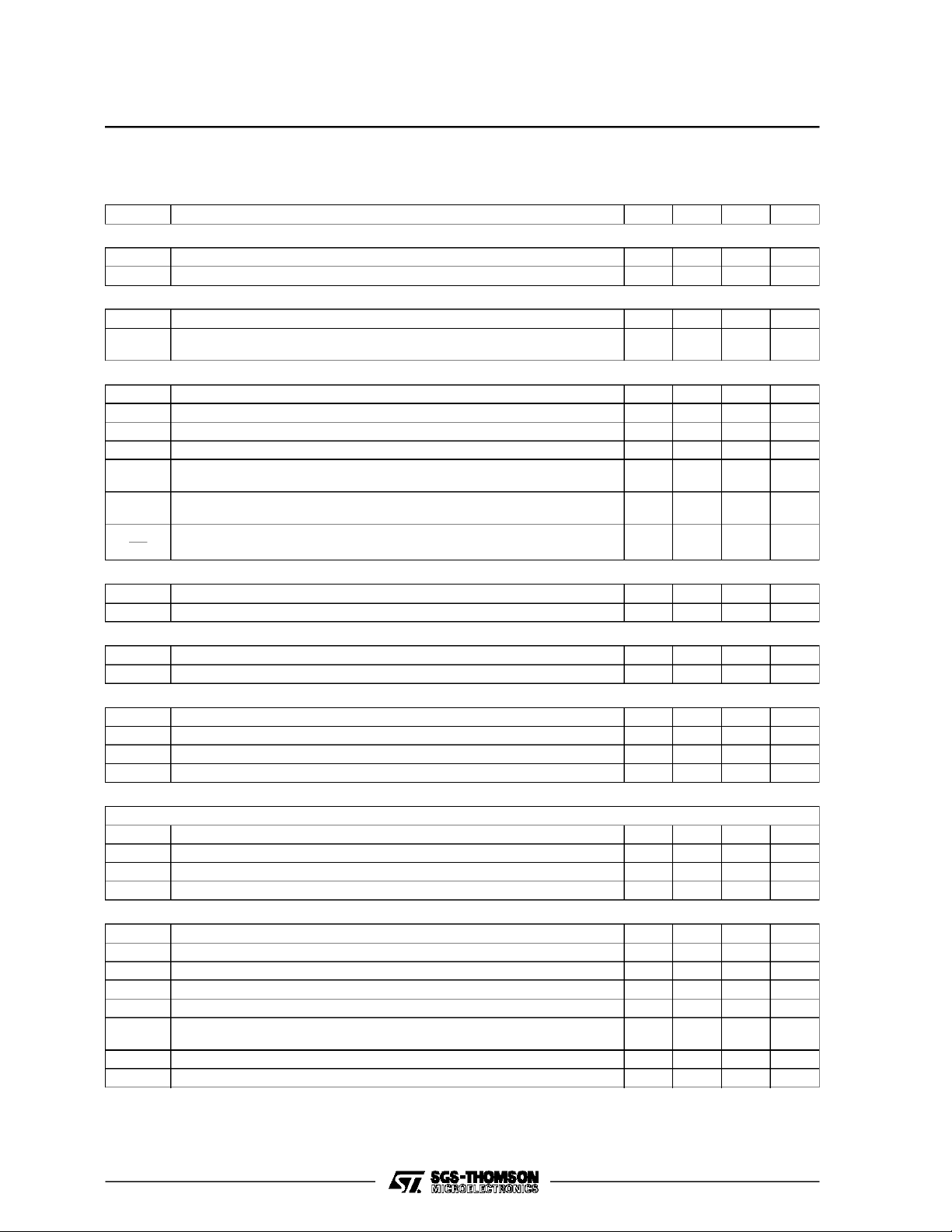
ABSOLUTE MAXIMUM RATINGS
Symbol Parameter Value Unit
1 Supply Voltage 30 V
V
CC
2 Flyback Generator Supply Voltage 35 V
V
CC
V9 Frame Power Supply Voltage 60 V
I10
I10 Frame Output Current (continuous) ± 1A
V17 Line Output Voltage(external) 60 V
17 Line Output Peak Current 0.8 A
I
P
17 Line Output Continuous Current 0.4 A
I
C
T
STG
T
T
AMB
Frame Output Current (non repetitive) ± 1.5 A
NR
Storage Temperature -40 to + 150
Max Operating Junction Temperature + 150
J
Operating Ambient Temperature 0 to 70
o
C
o
C
o
C
8218-02.EPS
8218-01.TBL
THERMALDATA
Symbol Parameter Value Unit
Max Junction-case Thermal Resistance 10
Typical Junction-ambient Thermal Resistance
(Soldered on a 35µm thick 45cm2PC Board copper area)
Max Recommended Junction Temperature 120
J
40
2/9
R
R
TH(j-c)
TH(j-a)
T
o
C/W
o
C/W
o
C
8218-02.TBL
TDA8218
ELECTRICAL CHARACTERISTICS
=10V,T
V
CC1
Symbol Parameter Min. Typ. Max. Unit
SUPPLY(Pin 1)
Supply Current 15 22 mA
Supply Voltage 9 10 10.5 V
CC1
V
I
CC1
VIDEO INPUT (Pin 20)
V20 Reference Voltage (I20 = -1µA) 1.4 1.75 2 V
MWF Minimum Width of Frame Pulse
(when synchronized with TTL signal)
LINE OSCILLATOR(Pin 11)
LT11 Low Threshold Voltage 2.8 3.2 3.6 V
HT11 High Threshold Voltage 5.4 6.6 7.8 V
BI11 Bias Current 100 nA
DR11 Discharge Impedance 1.0 1.4 1.8 kΩ
FLP1 Free Running Line Period
(R = 34.9kΩ Tied to V
OT11 Oscillator Threshold for Line Output
Pulse Triggering
∆F
Horizontal Frequency Drift with Temperature (see application) 2 Hz/
∆θ
LINE OUTPUT(Pin 17)
LV17 Saturation Voltage (I
OPW Output Pulsewidth (line period = 64µs) 26 28 30 µs
LINE SAWTOOTH INPUT (Pin 13)
V13 Bias Voltage 1.8 2.4 3.2 V
Z13 Input Impedance 4.5 5.8 8 kΩ
PHASE DETECTOR (Pin 12)
I12 Output CurrentDuring Synchro Pulse 250 350 500 µA
RI12 Current Ratio (positive/negative) 0.95 1 1.05
LI12 Leakage Current -2 +2 µA
CV12 Control RangeVoltage 2.60 7.10 V
FRAME BLANKING GENERATOR (Pin 8)
External R.C. Network (Typical values : R = 100kΩ, C = 22nF)
T
Blanking Time (PIn 19, Tfb= K8 .R.C.) 1.35 ms
fb
K8 Time Blanking Coefficient 0.588 0.613 0.644
I
Output Currentduring the Frame Blanking : V8= 2V - 0.2 1 µA
O8
I
Input Current after the Frame Blanking : V8= 7V 300 450 600 µA
I8
FRAME OSCILLATOR (Pin 2)
LT2 Low Threshold Voltage 1.6 2.0 2.3 V
HT2 High Threshold Voltage 2.6 3.1 3.6 V
DIF2 LT2- HT2 1.0 V
BI2 Bias Current 30 nA
DR2 Discharge Impedance 300 470 700 Ω
FFP1 Free Running Frame Period
(R = 866kΩ Tied to V
MFP Minimum Frame Period(I20 = -100µA) with the Same RC 12.8 ms
FPR Frame Period Ratio = FFP/MFP 1.7 1.8 1.9
=25oC (unlessotherwisespecified)
AMB
, C = 2.2nF Tied to Ground)
CC1
= 200mA) 1.1 1.6 V
17
1, C = 220nFTied to Ground)
CC
50 µs
62 64 66 µs
4.6 V
20.5 23 25 ms
o
C
8218-03.TBL
3/9

TDA8218
ELECTRICAL CHARACTERISTICS
=10 V,T
V
CC1
Symbol Parameter Min. Typ. Max. Unit
FRAME OSCILLATOR(Pin 2) (continued)
FG Frame Saw-tooth Gain Between Pin 1 and non Inverting Input of the
Frame Amplifier
∆F
Vertical Frequency Drift with Temperature(seeapplication) 4.10
∆θ
FRAME POWER SUPPLY(Pin 9)
V9 Operating Voltage (with flyback Generator) 10 58 V
I9 Supply Current (V9 = 30V) 9 15 mA
FLYBACK GENERATOR SUPPLY(Pin 3)
V
2 Operating Voltage 10 30 V
CC
FRAME OUTPUT (Pin 10)
Saturation Voltageto Ground (V9 = 30V)
LV10A I10 = 0.1A 0.06 0.6 V
LV10B I10 = 1A 0.37 1 V
Saturation Voltageto V9 (V9 = 30V)
HV10A I10 = -0.1A 1.3 1.6 V
HV10B I10 = -1A 1.7 2.4 V
Saturation Voltageto V9 in FlybackMode (V10 >V9)
FV10A I10 = 0.1A 1.6 2.1 V
FV10B I10 = 1A 2.5 4.5 V
FLYBACK GENERATOR (Pin 3 and Pin 4)
Flyback Transistor on (output = high state), V
F2DA
F2DB
I
4 → 3
I
4 → 3
Flyback Transistor on (output = high state), V
FSVA
FSVB
I
3 → 4
I
3 → 4
Flyback Transistor off (output = V9 - 8V), V9 - V
FCI Leakage Current Pin 3 170 µA
SUPER SANDCASTLE OUTPUT (Pin 19)
Output Voltages(R load= 2.2kΩ)
SANDT2 Frame blanking pulse level 2 2.5 3 V
SANDL2 Line blanking pulse level 4 4.5 5 V
BG2 Burst key pulse level 8 9 V
Pulses width and timing
SC3 Delay between middle of sync pulse and leading edge of burst key pulse 2.3 2.7 3.1 µs
SC2 Duration of burst key pulse
Vertical blanking pulse width : Defined by external R.C. Pin 8
LINE FLYBACK INPUT (Pin 18)
Switching level 2 V
Maximum imput current at V
Limiting voltage at maximum current 4.3 V
τ RC network time constant (Note 1) for the burst key pulse 6 µS
Note : 1. An RC network is connected to this input.Typical value for the resistor is 27kΩ and 220pF for the capacitor. A different time
constant forRC changes the delay between the middle of the line synchro pulse and theleading edge of the burst key pulse
but also the duration of the burst keypulse.
=25oC (unless otherwise specified )
AMB
= 0.1A
=1A
= 0.1A
=1A
= 800V 8 mA
PEAK
= 30V,V4/3 with
CC2
= 30V,V3/4 with
CC2
= 30V
CC2
-0.4
-3
1.5
3.0
0.8
2.2
Hz/oC
2.1
4.5
1.1
4.5
3.7 4 5 µs
V
V
V
V
8218-04.TBL
4/9

GENERALDESCRIPTION
The TDA8218 performs all the video and power
functions required to provide signals for the line
driverand frame yoke.
It contains:
• A synchronizationseparator
• An integrated frame separator without external
components
Figure1 : SynchronizationSeparatorCircuit
VR
Video
R1
TDA8218
• A saw-tooth generator for the frame
• A power amplifier for direct drive of frame yoke
(short circuitprotected)
• An opencollector outputfor the line driver
• A line phase detector and a voltage control os-
cillator
• A super sandcastle generator.
SL1
SL2
20
R2
The slice level of sync-separationis fixed by valueof the external resistorsR1 and R2. V
fixed voltage.
Figure2 : Frame Separator
Vz
I
SL1
3I
The sync-pulseallows thedischargeof thecapacitor by a 2 x I current. Aline sync-pulseis not able
to discharge the capacitor under V
/2. A frame
Z
Q3
/2
Vz
sync-pulse permits the complete dischargeof the
capacitor,so during the frame sync-pulse Q
providecurrent for the otherparts of the circuit.
Q
4
Q4
ST2ST1
isan internally
R
3
8218-03.EPS
8218-04.EPS
and
5/9

TDA8218
Figure3 : Line Oscillator
Vcc1
R5
11
Phase
comparator
output
R4
The oscillator thresholds are internally fixed by
resistors. The dischargeof the capacitor depends
on the internal resistor R4. The control voltage is
appliedon resistorR5.
The sync-pulse drives the currentin the comparator.The line flyback integrated by the external net
workgives on pin 13 a saw tooth, the DC offset of
this saw tooth is fixed by VC. The comparator
Figure4 : PhaseComparator
8218-05.EPS
output providesapositivecurrent for the partofthe
signalon pin 13greater than to VC and a negative
currentforthe other part.Whenthe line flybackand
the videosignalare synchronized,theoutputof the
comparatorisanalternativelynegativeandpositive
current. The frame sync-pulse inhibits the comparator to preventfrequency drift ofthe line oscillator
on the framebeginning.
Figure 5
Integrated
Flyback
Sync pulse
Output
Current
6/9
Line
Flyback
Vcc1
12
13
Vc
SL2
ST1
8218-06.EPS
Vc
8218-07.EPS

TDA8218
Line output (Pin 17)
It is an open-collector output. The output positive
pulsetimeis 28µsfor a 64µs period. The oscillator
thresholds are internally fixed by resistors. The
oscillator is synchronized during the last half free
run period. The input current during the charge of
the capacitoris less than 100nA.
Frame outputamplifier
This amplifier is able to drive directly the frame
yoke. Its output is short circuit and overload protected;it containsalso a thermalprotection.
The line flybackdetectionis provided by a comparator which compares the input line flyback pulse
to an internal reference. Theburst gate pulsepositionis fixed by the externalRC network (pin 14).It
Figure6 : Frame Oscillator
INPUT CURRENT
COMPENSATION
is referencedto themiddle of the line flyback.
The frameblankinggeneratoris a monostablewith
external R.C. The start blanking pulse is triggered
by the falling edge of the frame saw-tooth (Pin 2).
The resetis provided by a comparatorwhichcompares the capacitorvoltage during its charge to an
internal threshold fixed by resistors.
The frameblanking time is defined by:
T
=0.613 ⋅ R.C.
fb
ThispulseisavailableonSuperSandCastleoutput
(Pin 19).
Remark : For compatability with TEA5640, frame
blanking time must be larger than 1.15ms with
centered value @ 1.35ms (R = 100kΩ ± 1%,
C = 22nF ± 5%)
Vcc1
2
Figure7 : Super sandcastlegenerator
Flyback
Vcc1
R
Vcc1
C
BurstKey
RC
Network
Line
Input
18
8
14
To frameamplifier
Line
Flyback
Detection
Frame
Blanking
Generator
Σ
Burstgate
pulse
generator
RC
Vcc1
19
Frame
syncpulse
8218-08.EPS
SSC
Output
7/9
8218-09.EPS

TDA8218
TYPICALAPPLICATION
4.7
Vcc
+24V
Vcc1
Video
Input
Line
Flyback
27k
220pF
1.5k
120pF
100
Ω
220nF
Ω
560kΩ
15kΩ
68pF
100kΩ
180pF
Note : Pins 5 - 6 : Frame oscillator ground
Pins 15 - 16 :Frame and line power ground
Ω
100nF
µF
220nF
10%
14
20
22nF
13
22nF
18
4.7kΩ
1µF
100nF
866kΩ
21 8 39 4
22nF
5%
470µF
100k
1%
IN4002
Ω
47µF
10
TDA 8218
7
12
100k
12nF
11 5 6
Ω
2.2nF
22kΩ
Vcc1
22kΩ
Horizontal
Frequency
15
16
SSC
19 17
2.2kΩ
680pF
Vcc1
100
IN4148
220k
Vertical
Ω
Amplitude
22kΩ
100nF
FrameYoke
30 mH,15
I = 840mA
pp
Ω 220kΩ
220nF
100Ω
2.2Ω
Ω
270Ω
1000µF
1Ω
8218-10.EPS
8/9

PACKAGE MECHANICAL DATA
20 PINS - POWERDIP16 + 2+ 2
TDA8218
I
a1
L
Z
Dimensions
b
e3
20 11
110
B
D
Millimeters Inches
Min. Typ. Max. Min. Typ. Max.
e
Z
F
E
a1 0.51 0.020
B 0.85 1.4 0.033 0.055
b 0.5 0.020
b1 0.38 0.5 0.015 0.020
D 24.8 0.976
E 8.8 0.346
e 2.54 0.100
e3 22.86 0.900
F 7.1 0.280
i 5.1 0.201
L 3.3 0.130
Z 1.27 0.050
b1
PMDIP20W.EPS
DIP20PW.TBL
Information furnished is believed tobe accurate andreliable. However, SGS-THOMSON Microelectronics assumes no responsibility
for the consequences of useof suchinformation nor forany infringement ofpatents or other rights of third partieswhich may result
from itsuse. No licence is granted byimplication or otherwiseunder anypatent or patent rights ofSGS-THOMSON Microelectronics.
Specifications mentioned in this publication are subject to change without notice. This publication supersedes and replaces all
information previously supplied.SGS-THOMSON Microelectronics products are not authorized for useas critical components in life
support devices or systems withoutexpress written approval of SGS-THOMSON Microelectronics.
1994 SGS-THOMSON Microelectronics - All Rights Reserved
2
Purchase of I
2
I
C Patent. Rights to use these components in a I2C system,is granted provided that thesystem conforms to
Australia - Brazil - China - France - Germany - Hong Kong - Italy - Japan - Korea- Malaysia - Malta - Morocco
The Netherlands- Singapore - Spain - Sweden - Switzerland - Taiwan - Thailand - United Kingdom - U.S.A.
C Components of SGS-THOMSON Microelectronics, conveys a license under the Philips
2
the I
C Standard Specificationsas defined by Philips.
SGS-THOMSON Microelectronics GROUP OF COMPANIES
9/9
 Loading...