


TDA7511
AM/FM TUNER FOR CAR RADIO AND HIFI APPLICATIONS
FM-PART
■ RF AGC GENERATION BY RF AND IF
DETECTION FOR PIN DIODES AND MOSFET
(PRESTAGE)
ST
■ 1
MIXER FOR 1ST FM IF 10.7MHz WITH
PROGRAMMABLE IF TANK ADJUST FOR FM
AND AM UPCONVERSION
■ 2 PROGRAMMABLE IF-GAIN STAGES
ND
■ 2
MIXER FOR 2ND IF 450KHz
■ INTERNAL IF BANDPASS FILTER WITH
THREE BANDWIDTHS CONTROLLED BY ISS
(INCLUDING WEATHER BAND)
■ FULLY INTEGR ATED FM-DEMODULATOR
AM-PART
■ WIDE AND NARROW AGC GENERATION
■ PREAMPLIFIER AND MIXER FOR 1ST IF
10.7MHZ,
AM UPCONVERSION
ND
■ 2
MIXER FOR 2ND IF 450KHZ
■ INTEGRATED AM-DEMODULATOR
■ OUTPUT FOR AM-STEREO-DECODER
ORDERING NUMBER: TDA7511
MULTIPATH
■ QUALITY DETECTION INFORMATIONS AS
ANALOG SIGNALS EXT ERN AL AVAIL ABLE
■ ISS (INTELLIGENT SELECTIVITY SYSTEM)
FOR CANCELLATION OF ADJACENT
CHANNEL AND NOISE INFLUENCES
■ ADJACENT CHANNEL MUTE
■ FULLY ELECTR ONIC ALIGNMENT
■ ALL FUNCTIONS I
■ ISS FILTE R STATUS I NFORMATION I
READABLE
TQFP64
2
C-BUS CONTROLLED
2
C-BUS
ADDITIONAL FEATURES
■ HIGH PERFORMANCE FAST PLL FOR RDS-
SYSTEM
■ IF COUNTER FOR FM AND AM
UPCONVERSION WITH SEARCH STOP
SIGNAL
■ QUALITY DETECTOR FOR LEVEL,
DEVIATION, ADJACENT CHANNEL AND
November 2001
DESCRIPTION
The TDA 7511 is a high performance tuner circuit for
AM/FM car radio. It contains mixers, IF amplifiers, demodulators for AM and FM, quality detection, ISS filter and PLL synthesizer with IF counter on a single
chip.
Use of BICMOS technology allows the implementation of several tuning function s and a mini mum of external components.
1/41
TDA7511
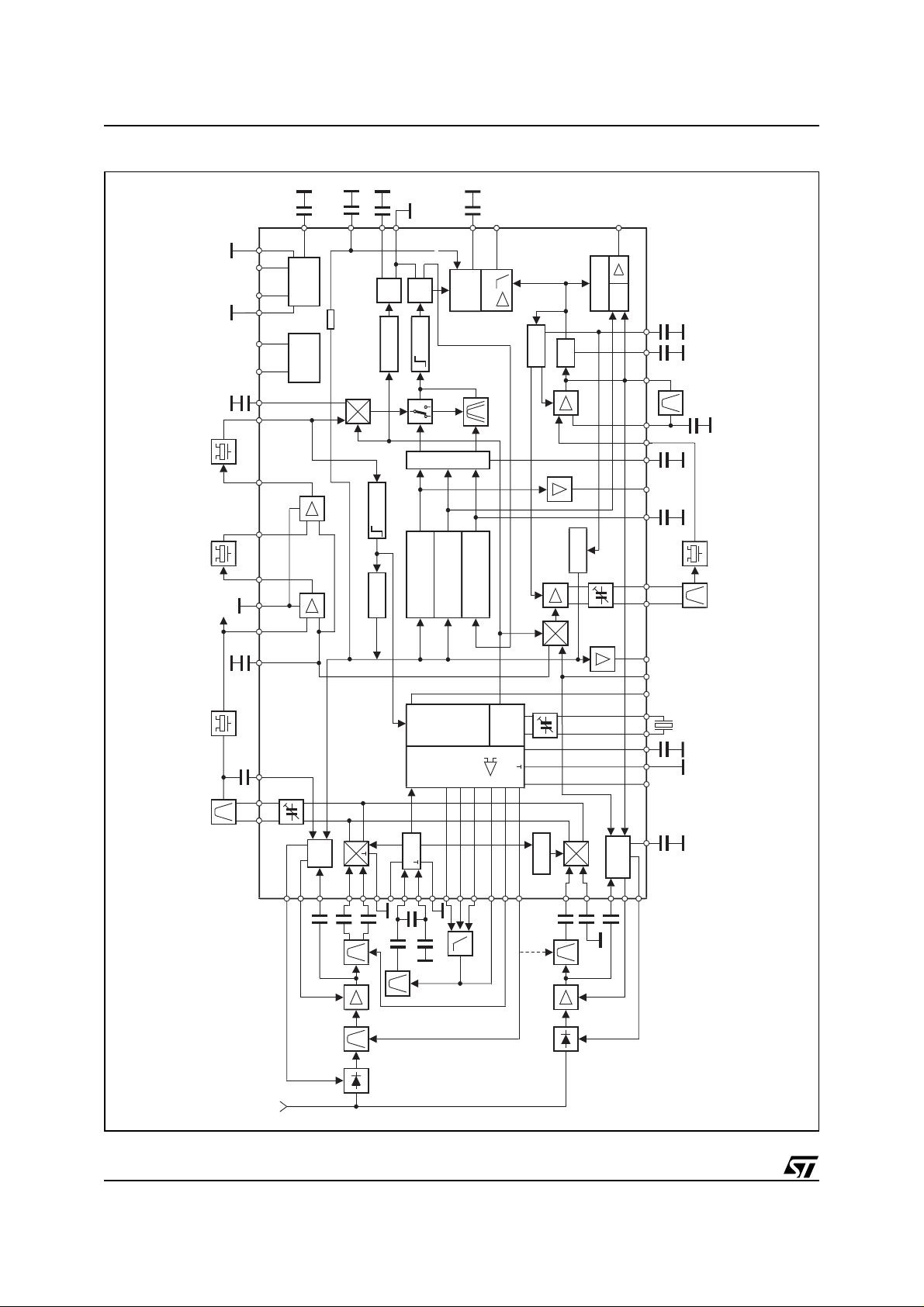
BLOCK DIAGRAM
AMIFin
48
V
V
25 26 33 36 51 49
57 59 54 52 50 46 45
53
CC2
CC1
C Bus
2
I
Supply
35
44
47
REF
Dem
Dem
MPX
450KHz
Divider
Logic
Multipath
Detection
S-Meter 10.7MHz
Adjacent Channel
42
Mute
Soft/AC
Deviation
Detection
Detection
AF
37
DAGC
Dem
ISS
Stopstation
S-Meter
34
MUX
15 43 38 39 41 40
55 56 20 13
AMIF1in
IFC
PLL
PD
61 62 60
PIN
VCO
+
303132
181916178
AGC
7
9
11
6
5
FM
CP
Xtal
281012
CC3
27 2123 20 22 24 58 14
+
Divider
1
PIN
AM
2
WAGC
3464
V
63
99A T0052
2/41
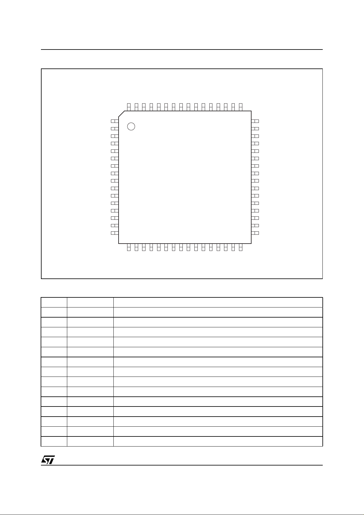
TDA7511
PIN CONNECTION
AMRFAGCIN
AMRFAGCOUT
FMRFAGCIN
(Top view)
AMMIX1IN2
AMMIX1IN1
FMPINDR
FMMOSDR
FMMIX1IN1
GNDRF
FMMIX1IN2
TV1
TV2
ADJCH
FSU
ISSTC
VCCVCO
AMPINDR
AMRFAGCTC
MIX1OUT1
MIX1OUT2
64 63 62 61 60 59 58 57 56 55 54
1
2
3
4
5
6
7
8
9
10
11
12
13
14
15
16
20
1918
17
21
FMIFAGCIN
GNDIFAMP
AMIF1IN
24
2322
FMAMP1IN
25
AMMIX2OUT1
FMIF1REF
AMMIX2OUT2
FMAMP1OUT
53
27
26
28
FMAMP2IN
VCC2
52
51
29
30
GNDVCC2
FMAMP2OUT
50 49
48
47
46
45
44
43
42
41
40
39
38
37
36
35
34
33
31 32
VREF1
GNDDEM
FMMIX2IN1
FMMIX2IN2
FMDEMC
AMIF2IN
MUTETC
AMDETC
AMAGC2TC
AMIFBPF
AMIFREF
MPX/AFAM
VCC1
FSW
AMST/MP
GNDVCC1
SCL
SDA
99AT0053
PIN DESCRIPTION
(continued)
GNDVCO
VCOB
VCOE
XTALD
DEVTC
XTALG
SSTOP
GNDVCC3
VCC3
N° Pin Function
1 AMMIX1IN2 AM Input2 Mixer1
2 AMMIX1IN1 AM Input1 Mixer1 Reference
3 AMRFAGCIN Input AM RF AGC
4 AMRFAGCOUT Output AM RF AGC
5 FMPINDR FM PIN Diode Driver Output
6 FMMOSDR FM MOS Driver Output
7 FMMIX1IN1 FM Input1 Mixer1
8 GNDRF RF Ground
9 FMMIX1IN2 FM Input2 Mixer1
10 TV1 Tuning Voltage 1
11 FMRFAGCIN FM RF AGC Input
12 TV2 Tuning Voltage 2
13 ADJCH Ident. Adjacent Channel Output
14 FSU Unweighted Fieldstrength Output
VREF2
LPOUT
LPAM
LPFM
LPHC
3/41

TDA7511
PIN DESCRIPTION
N° Pin Function
15 ISSTC Time Constant for ISS Filter Switch
16 VCCVCO VCO Supply
17 GNDVCO VCO Ground
18 VCOB VCO Input Base
19 VCOE VCO Output Emitter
20 DEVTC Deviatio n Detector Time Cons tant
21 XTALD Xtal Oscillator to MOS Drain
22 XTALG Xtal Oscillator to MOS Gate
23 GNDVCC3 VCC3 Ground
24 SSTOP Se arch Stop Outpu t
25 SDA
26 SCL
27 VCC3 Supply Tuning Voltage
28 LPOUT Op Amp Output to PLL Loop Filters
29 VREF2 Voltage Reference for PLL Op Amp
30 LPAM Op Amp Input to PLL Loop Filters AM
31 LPFM Op Amp Input to PLL Loop Filters FM
32 LPHC High Current PLL Loop Filter Input
33 GNDVCC1 Digital Ground
34 AMST/MP AM Stereo Out / Ident. Multipath Output
35 FSW Weighted Fieldstrength Output
36 VCC1 Digital Supply
37 MPX/AFAM MPX Output / AM AF Output
38 AMIFREF Reference Voltage AM IF Amp
39 AMIFBPF AM IF Filter
40 AMAGC2TC AM AGC2 Time Constant
41 AMDETC AM Detector Capacitor
42 MU TETC Softmute Time Constant
43 AMIF2IN Input AM IF2
44 FMDEMC FM Demodulator Reference
45 FMMIX2IN2 FM IF1 MIX2 Input1
46 FMMIX2IN1 FM IF1 MIX2 Input2
47 GNDDEM Ground FM Demodulator
48 VREF1 Reference 5V
49 GNDVCC2 Analog Ground
50 FMAMP2OUT FM IF1 Amplifier2 Output
(continued)
2
I
2
I
C-Bus Data
C-Bus Clock
4/41
TDA7511
PIN DESCRIPTION
(continued)
N° Pin Function
51 VCC2 Analog Supply
52 FMAMP2IN FM IF1 Amplifier2 Input
53 FMIF1REF FM IF1 Amplifier Reference
54 FMAMP1OUT FM IF1 Amplifier1 Output
55 AMMIX2OUT2 AM Tank 450kHz
56 AMMIX2OUT1 AM Tank 450kHz
57 FMAMP1IN FM IF1 Amplifier1 Input
58 AMIF1IN AM IF1 Input
59 GNDIF1AMP FM IF1 Amplifier Ground
60 FMIF1AGCIN FM IF1 AGC Input
61 MIX1OUT2 MIX Tank 10.7MHz
62 MIX1OUT1 MIX Tank 10.7MHz
63 AMRFAGCTC AM RF AGC Time Constant
64 AMPINDR AM PIN Diode Driver Output
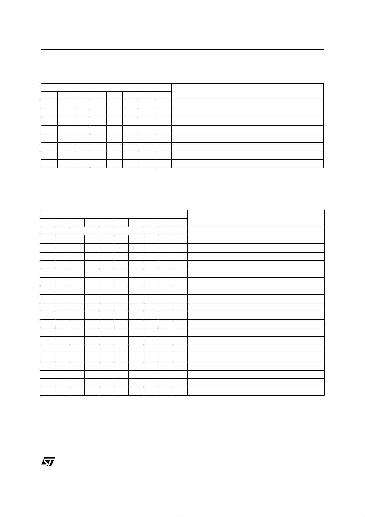
ABSOLUTE MAXIMUM RATINGS
Symbol Parameter Value Unit
V
T
amb
T
stg
Supply Voltage 10.5 V
S
Ambient Temperature -40 to 85 °C
Storage Temperature -55 to +150 °C
THERMAL DATA
Symbol Parameter Value Unit
R
Th(j-amb)
Thermal resistance 68 °C/W
ELECTRICAL CHARACTERISTCS
T
amb
f
MOD
= +25°C,
=1kHz, f
V
=
V
CC1
= 10.7MHz, f
IF1
CC2
=
V
CC3
=
V
CCVCO
= 450KHz, f
IF2
=
V
Xtal
= 8.5V, fRF= 98MHz, dev. = 40kHz,
CCMIX1
= 10.25MHz, in test or application circuit, unless otherwise
specified.
Symbol Parameter Test Condition Min. Typ. Max. Unit
Supply
V
V
V
V
CCVCO
Digital supply voltage 7.5 8.5 10 V
CC1
Analog supply voltage 7.5 8.5 10 V
CC2
Analog tuning voltage 7.5 8.5 10 V
CC3
VCO supply voltage 7.5 8.5 10 V
5/41
TDA7511
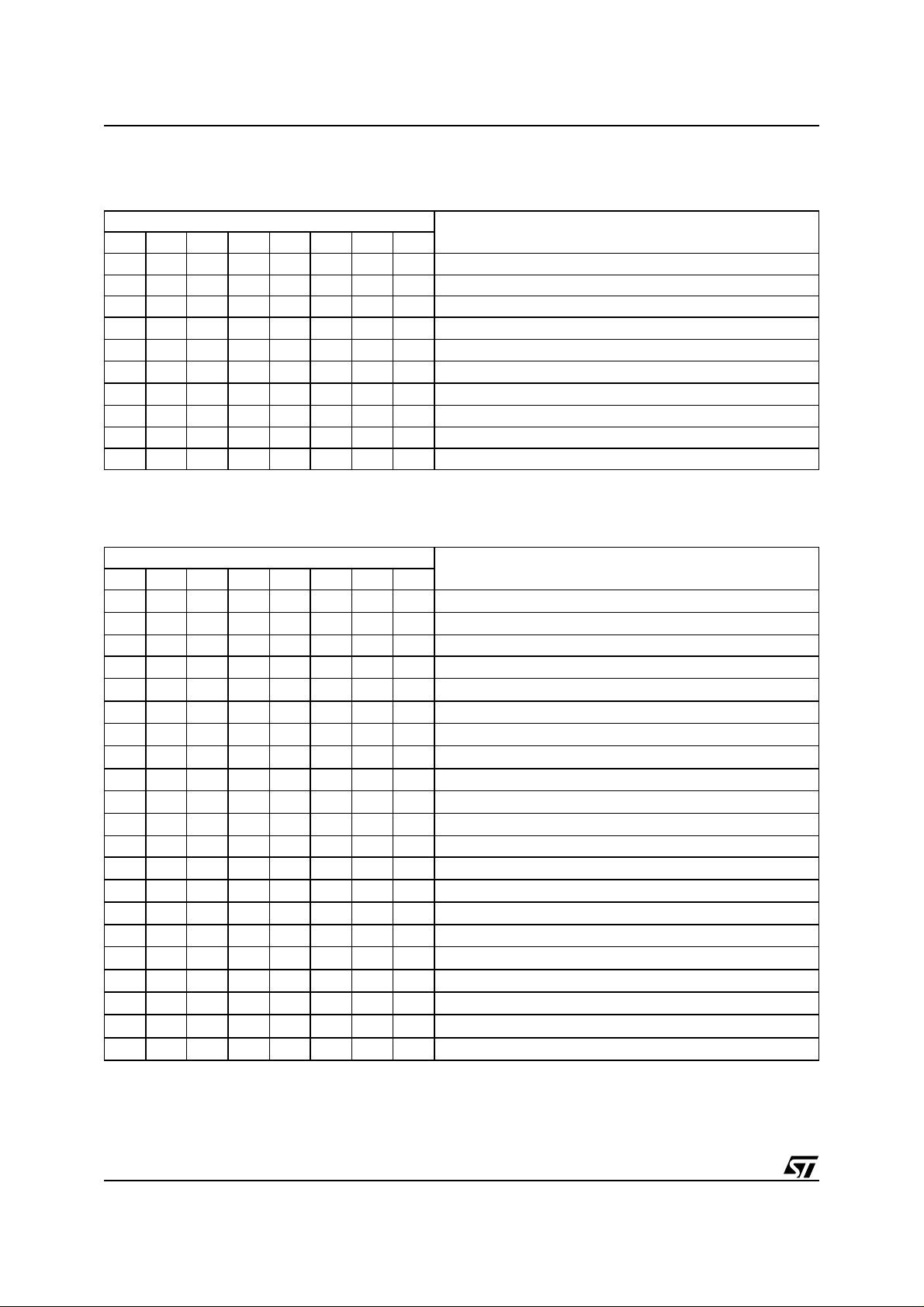
ELECTRICAL CHARACTERISTCS
T
amb
f
MOD
= +25°C,
=1kHz, f
V
=
V
CC1
= 10.7MHz, f
IF1
CC2
=
V
(continued)
=
V
CC3
= 450KHz, f
IF2
CCVCO
=
V
Xtal
= 8.5V, fRF= 98MHz, dev. = 40kHz,
CCMIX1
= 10.25MHz, in test or application circuit, unless otherwise
specified.
Symbol Parameter Test Condition Min. Typ. Max. Unit
V
CCMIX1
V
CCMIX2
I
CC1
I
CC1
I
CC2
I
CC2
I
CC3
I
CCVCO
I
CCMIX1
I
CCMIX1
I
CCMIX2
Reference Voltages
V
REF1
V
REF2
Wide Band RF AGC
V
R
C
Narrow Band RF & Keying AGC
V
V
R
C
AGC MOSFET Driver Output
V
V
AGC PIN Diode Driver Output
Mixer1 (10.7MHz)
R
MIX1 supply voltage 7.5 8.5 10 V
MIX2 supply voltage 7.5 8.5 10 V
Supply current FM ON 7.5 mA
Supply current AM ON 10 mA
Supply current FM ON 50 mA
Supply current AM ON 60 mA
Supply current 2 mA
Supply current 2.5 mA
Supply current FM ON 6 mA
Supply current AM ON 5 mA
Supply current AM ON 5 mA
Internal reference voltage I
Internal reference voltage I
Threshold AGC start V6 = V
11
Input resistance 500
IN
Input capacitanc e 2.5 pF
IN
Lower threshold FMAGC, V11 = 0mV
60
Upper threshold FMAGC, V11 = 0mV
60
Input resistance 10
IN
Input capacitanc e 2.5 pF
IN
Max. AGC output voltage V11 = 0mV
6
= 0mA 5 V
REF1
= 0mA 2.5 V
REF2
/2 80
CC2
82
92
RMS
RMS
RMS
V
CC2
-0.5V
Min. AGC output voltage V11 = 50mV
6
I
Min. AGC charge current V11 = 0mV
6
Max. AGC discharge current V11 = 50mV
I
6
AGC OUT, current min. V11 = 0mV
I
5
I
AGC OUT, current max. V11 = 50 mV
5
Input impedance B alanc ed, f = 98MHz 9
IN
RMS
= V
RMS,V6
RMS,V6
, V5 = 2V 50
RMS
, V5 = 2V -6 mA
RMS
/2 -12.5
CC2
= V
/2 1.25 mA
CC2
dB
dB
dB
0.5 V
Ω
k
V
µA
µA
Ω
µV
µV
µV
Ω
6/41
TDA7511
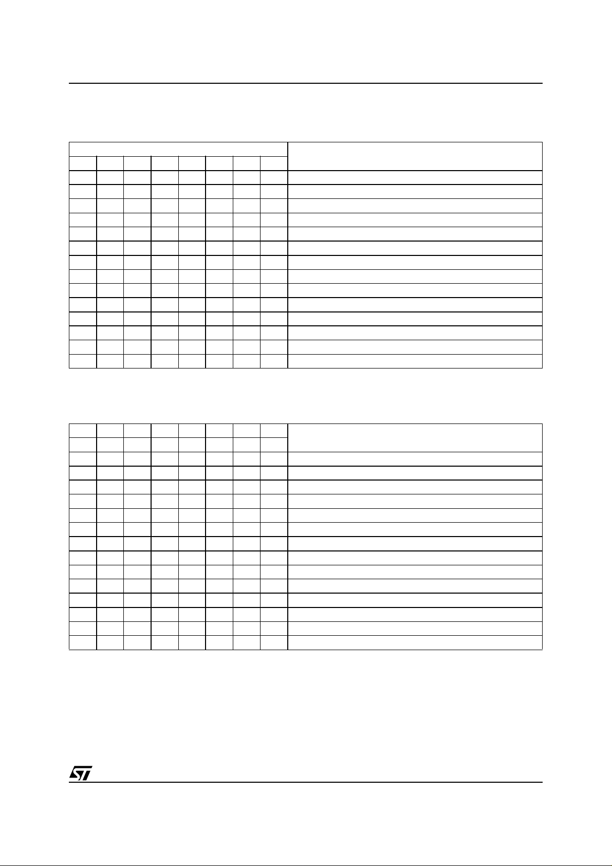
ELECTRICAL CHARACTERISTCS
T
amb
f
MOD
= +25°C,
=1kHz, f
V
=
V
CC1
= 10.7MHz, f
IF1
CC2
=
V
(continued)
=
V
CC3
= 450KHz, f
IF2
CCVCO
=
V
Xtal
= 8.5V, fRF= 98MHz, dev. = 40kHz,
CCMIX1
= 10.25MHz, in test or application circuit, unless otherwise
specified.
Symbol Parameter Test Condition Min. Typ. Max. Unit
IP3 3rd order intercept point 122
F N oise figure 6dB
A
Conversion gain 120 mS
C
IF1 Amplifier1 & 2 (10.7MHz)
A
A
R
R
P
Min. gain IFG 9 dB
min
Max. gain IFG
max
Input resistance 330
IN
Output resistance 330
OUT
1dB compression point Output referred 120
1dB
15
IP3 3rd order Intercept Point Output referred 132
Mixer2 (450kHz)
R
V
V
Input impedance 330
IN
Max. input voltage 900 mV
46
Limiting sensitivity S/N = 20dB 25
48
A Mixer gain 18 dB
Limiter 1 (450kHz)
G
Limiter
Gain 80 dB
Demodulator, Audio Output
THD Dev.= 75kHz, V
V
R
|∆V|
∆V|
|
MPX
MPX output signal Dev.= 75kHz 500 mV
Output resistance 350
OUT
DC offset fine adjust DEM, MENA=1 6 mV
min
DC offset fine adjust DEM, MENA=1 186 mV
max
S/N Dev.= 40kHz,V
= 10mV
46
= 10mV
46
RMS
RMS
0.1 %
75 dB
Quality Detection
S-meter, Unweighted Fieldstrength
V
∆V
∆V
V
V
R
Min. input voltage MIX2 10
46
Per decade SMSL = 0 1 V
Per decade SMSL = 1 1.5 V
Fieldstrength output V46 = 0V
14
Fieldstrength output V46 = 1V
14
Output resistance 4
OUT
RMS
RMS
0.1 V
4.9 V
dB
dB
dB
dB
Ω
Ω
Ω
µV
Ω
µV
k
µV
µV
µV
RM
S
RM
S
Ω
7/41
TDA7511
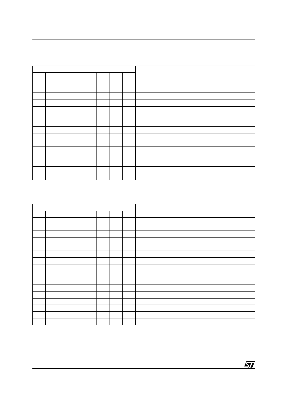
ELECTRICAL CHARACTERISTCS
T
amb
f
MOD
= +25°C,
=1kHz, f
V
=
V
CC1
= 10.7MHz, f
IF1
CC2
=
V
(continued)
=
V
CC3
= 450KHz, f
IF2
CCVCO
=
V
Xtal
= 8.5V, fRF= 98MHz, dev. = 40kHz,
CCMIX1
= 10.25MHz, in test or application circuit, unless otherwise
specified.
Symbol Parameter Test Condition Min. Typ. Max. Unit
∆V
TK Temp coeff. 0 ppm/K
S-meter, Weighted Fieldstrength
V
V
R
Adjacent Channel Gain
A
A
Adjacent Channel Filter
f
f
f
-20dB
Adjacent Channel Output
V
V
R
Multipath Channel Gain
A
A
Multipath Bandpass Filter
f
Lower
f
Upper
Multipath Output
V
V
R
ISS (intelligent Selectivity System)
Filter 450kHz
f
centre
BW 3dB Bandwidth, -3dB ISS80 = 1 80 kHz
BW
20dB
S-meter shift voltage SL -1.8 1.8 V
14
Fieldstrength output V46 = 0V
35
Fieldstrength output V46 = 1V
35
Output resistance 12
OUT
Gain minimum ACG 32 dB
min
Gain maximum ACG 38 dB
max
-3dB frequency highpass ACF 100 kHz
HP
Centre frequency ACF 100 kHz
BP
RMS
RMS
2.5 V
4.9 V
Attenuation 20dB 70 kHz
Output voltage low 0.1 V
13
Output voltage high 4.9 V
13
Output resistance 4
OUT
Gain minimum MPG 12 dB
min
Gain maximum MPG 23 dB
max
Centre frequency low MPF 19 kHz
Centre frequency up MPF 31 kHz
Q Quality factor 5 10
Output voltage low 0.1 V
34
Output voltage high 4.9 V
34
Output resistance 2.5
OUT
Centre frequency f
REF_intern
= 450kHz 450 kHz
Bandwidth, -20dB ISS80 = 1 150 kHz
Ω
k
Ω
k
Ω
k
8/41
TDA7511
ELECTRICAL CHARACTERISTCS
T
amb
f
MOD
= +25°C,
=1kHz, f
V
=
V
CC1
= 10.7MHz, f
IF1
CC2
=
V
(continued)
=
V
CC3
= 450KHz, f
IF2
CCVCO
=
V
Xtal
= 8.5V, fRF= 98MHz, dev. = 40kHz,
CCMIX1
= 10.25MHz, in test or application circuit, unless otherwise
specified.
Symbol Parameter Test Condition Min. Typ. Max. Unit
BW 3dB Bandwidth, -3dB ISS80 = 0 120 kHz
BW
20dB
BW 3dB Bandwidth weather band ISS30 = 1 30 kHz
BW
20dB
∆f
∆f
Adjacent Channel ISS Filter Threshold
V
V
V
WTH
V
WTH
Multipath Threshold
V
THMP
V
THMP
ISS Filter Time Constant
I
I
I
I
I
I
V
V
ISS Filter Switch Threshold
V
V
V
V
I
I
I
I
Bandwidth, -20dB ISS80 = 0 250 kHz
-20dB weather band ISS30 = 1 80 kHz
Fine adjust AISS -20 kHz
min
Fine adjust AISS 10 kHz
max
Internal low threshold ACNTH 0 V
NTH
Internal high threshold ACNTH 0.3 V
NTH
Internal low threshold ACWTH 0.25 V
Internal high threshold ACWTH
0.95
Internal low threshold MPTH 0.50 V
Internal high threshold MPTH 1.25 V
Charge current low mid TISS, ISSCTL = 1 -74
15
Charge current high mid TISS, ISSCTL = 1 -60
15
Charge current low narrow TISS, ISSCTL = 1 -124
15
Charge current high narrow TISS, ISSCTL = 1 -110
15
Discharge current low TISS, ISSCTL = 0
15
Discharge current high TISS, ISSCTL = 0 15
15
Low voltage ISSCTL = 0 0.1 V
15
High voltage ISSCTL = 1 4.9 V
15
Threshold ISS on ISSCTL = 0 3 V
15
Threshold ISS off ISSCTL = 0 1 V
15
Threshold ISS narrow on ISSCTL = 0 4 V
15
Threshold ISS narrow off ISSCTL = 0 2 V
15
Charge current low TDEV -20
20
Charge current high TDEV -34
20
Discharge current low TDEV 6
20
Discharge current high TDEV 20
20
1
V
µA
µA
µA
µA
µA
µA
µA
µA
µA
µA
9/41
TDA7511
ELECTRICAL CHARACTERISTCS
T
amb
f
MOD
= +25°C,
=1kHz, f
V
=
V
CC1
= 10.7MHz, f
IF1
CC2
=
V
(continued)
=
V
CC3
= 450KHz, f
IF2
CCVCO
=
V
Xtal
= 8.5V, fRF= 98MHz, dev. = 40kHz,
CCMIX1
= 10.25MHz, in test or application circuit, unless otherwise
specified.
Symbol Parameter Test Condition Min. Typ. Max. Unit
DEV
DEV
RATIO
RATIO
Softmute
V
V
a
SMmin
a
SMmax
a
SMTHIS
V
ACTH
a
SMAC
I
I
S/N Over All
S/N
Internal low threshold DWTH 30 kHz
WTH
Internal high threshold DWTH 75 kHz
WTH
Referred to threshold DTH 1
mi
n
Referred to threshold DTH 1.5
m
ax
Upper startpoint SMTH, SMD, SLOPE = 0 16
ANT
lower startpoint
ANT
Min. softmute depth SMD, SLOPE = 0, SMTH
Max. softmute depth SMD, SLOPE = 0, SMTH
SMTH, SMD, SLOPE = 0 3
Upper
Upper
18 dB
36 dB
Mute depth threshold for ISS filter onSMCTH 0.2 2 dB
S
Internal AC mute threshold ACM 60 220 mV
AC mute depth 6 dB
Charge current -47.5
42
Discharge current 2.5
42
V
IN_min
= 60dBµV,
66 dB
dev.= 40kHz,LP=15KHz
deemphasis t = 50
µs
dB
dB
µV
µV
µA
µA
ELECTRICAL CHARACTERISTICS
T
amb
AMf
= +25°C,
= 10.7MHz, f
IF1
V
=
V
CC1
IF2
=
CC2
= 450kHz, f
V
=
CC3
V
xtal
=
CCVCO
V
CCMIX1
=
V
CCMIX2
=8.5V, fRF=1MHz, f
= 400Hz at 30%
MOD
= 10.25MHz, in test or application circuit, (unless otherwise noted, V
antenna input).
Symbol Parameter Test Condition Min. Typ. Max. Unit
AM SECTION
Global
INRF
Max. sensitivity
Ref.: V
∆V
37
= 74dBµV,
INRF
= -10dB
us Usable sensitivity (S+N)/N = 20 dB 30 26
INRF
AGC Range
Ref.: V
∆V
37
Ref.: V
= 74dBµV,
INRF
= -10dB
= 74dBµV
INRF
V
min
V
INRF
∆V
(S+N)/N Signal to Noise Ratio
10/41
51 dB
49 56 dB
19
dB
dB
inRF
µV
µV
TDA7511
ELECTRICAL CHARACTERISTICS
T
amb
AMf
= +25°C,
= 10.7MHz, f
IF1
V
=
V
CC1
IF2
=
CC2
= 450kHz, f
V
CC3
(continued)
=
V
xtal
=
CCVCO
V
CCMIX1
=
V
CCMIX2
=8.5V, fRF=1MHz, f
= 400Hz at 30%
MOD
= 10.25MHz, in test or application circuit, (unless otherwise noted, V
antenna input).
Symbol Parameter Test Condition Min. Typ. Max. Unit
a
a
f
V
INRFSS
THD Total Harmonic Distortion
V
V
IF rejection
IF
Tweet
TW
Frequency response
AF
Ref: V
IF1 = 10.7MHz
IF2 = 450kHz
∆V
C
28
Ref.: V
∆V
INRF
= -10dB
37
= 22µF
INRF
= -3 dB
AF
= 74dBµV,
100
100
-3 -0.7 dB
= 74dBµV,
Seek Stop Sensitivity A MSS 20 35 45
V
= 74 dBµV, m = 0.8
INRF
m = 0.3
= 120 dbµV, m = 0.8
V
INRF
m = 0.3
37
34
Output level
Output level
= 74 dBµV
V
INRF
= 74 dBµ, m=off
V
INRF
3.6 kHz
dB
0.5
0.3
1.0
0.3
220 mV
190 mV
inRF
dB
dB
µV
%
RM
S
RM
S
V
R
63OUT
R
40OUT
R
40OUT
V
V
Min. RF AGC threshold
3
Max. RF AGC threshold
Min. IF AGC threshold
58
Max. IF AGC threshold
Min. IF AGC threshold
3
Max. IF AGC threshold
AMAGC
Wide
AMAGC
Middle
DAGC
Narrow
Output impedance 100
Output impedance AMSEEK = 0 150
Output impedance AMSEEK = 1 5
AGC Voltage Driver Output
V
V
Max. AGC output voltage 3.5 V
4
Min. AGC output voltage
4
|I4| AGC current 100
AGC PIN Diode Driver Output
I
AGC driver current 1.5 mA
64
AM Mixer1 (10.7MHz)
R
Input impedance 1.2
IN
82
98.8
80.1
96.8
32.6
80.7
0.5
dB
dB
dB
dB
dB
dB
k
k
k
V
µA
k
µV
µV
µV
µV
µV
µV
Ω
Ω
Ω
Ω
IP3 3rd order intercept point 140
dB
µV
F N oise figure 7dB
11/41
TDA7511
ELECTRICAL CHARACTERISTICS
T
amb
AMf
= +25°C,
= 10.7MHz, f
IF1
V
=
V
CC1
IF2
=
CC2
= 450kHz, f
V
CC3
(continued)
=
V
xtal
=
CCVCO
V
CCMIX1
=
V
CCMIX2
=8.5V, fRF=1MHz, f
= 400Hz at 30%
MOD
= 10.25MHz, in test or application circuit, (unless otherwise noted, V
inRF
antenna input).
Symbol Parameter Test Condition Min. Typ. Max. Unit
A Gain 6dB
C
C
C
61-62
AM Mixer2 (450kHz)
R
IP3 3rd order intercept point 140
∆A
C
C
Min. capacitance step IF1T 0.55 pF
min
Max. capacitance IF1T 8.25 pF
max
IF1T 2 pF
Input impedance Dependent on application 5
IN
k
dB
F N oise figure 12 dB
A Max. gain Mixer2 tank output 15 dB
Gain control range 20 dB
Min. cap step IF2T 1.6 pF
min
Max. cap IF2T 24 pF
max
Ω
µV
C
55-56
ELECTRICAL CHARACTERISTICS
IF2T 2 pF
Symbol Parameter Test Condition Min. Typ. Max. Unit
ADDITIONAL PARAMETERS
Outputs of Tuning Voltage(TV1, TV2)
V
R
Output voltage TVR,TVO 1 VCC3-1VV
OUT
Output impedance 20
OUT
Xtal Reference Oscillator
f
C
C
∆f/f
∆f/f
2
I
C-Bus interface
f
SCL
Reference frequency C
LO
Min. cap step XTAL 0.6 pF
Step
Max. cap XTAL 19.4 pF
max
Freq. deviation versus VCC2
= 15pF 10.25 MHz
Load
∆V
CC2
= 1V
1.5 ppm/V
Freq. deviation versus temp -40°C < T < +85°C 0.2 ppm/K
Clock frequency 400 kHz
Ω
k
12/41
V
Input low voltage 1V
IL
TDA7511
ELECTRICAL CHARACTERISTICS
(continued)
Symbol Parameter Test Condition Min. Typ. Max. Unit
V
I
V
Input high voltage 3 V
IH
Input current -5 5
IN
Output voltage SDA acknowledge IO = 1.6mA 0.4 V
O
Loop Filter Input/Output
-I
I
V
V
I
OUT
I
OUT
Input leakage current VIN = GND, PD
IN
Input leakage current VIN = VREF1
IN
Output voltage Low I
OL
Output voltage High I
OH
Output current, sink V
Output current, source V
PD
= Tristate
OUT
= -0.2mA 0.05 0.5 V
OUT
= 0.2mA VCC3
OUT
= 1V to V
OUT
= 1V to V
OUT
= Tristate -0.1 0.1
OUT
-0.1 0.1
VCC3
-0.5
-1V 10 mA
CC3
CC3
-1V
-10
-0.05
Voltage Controlled Oscillator (VCO)
f
VCOmin
f
VCOmax
Minimum VCO frequency
Maximum VCO frequency 200 MHz
50
µA
µA
µ
A
V
mA
MHz
C/N Carrier to Noise 1KHz offset 85 dBc
SSTOP Output
V
V
V
Output voltage low
24
Output voltage high
24
IF counter sensitivity Antenna input 6
46
= -20µA
I
24
= 20µA
I
24
3V
0.2 V
dB
µV
13/41

TDA7511
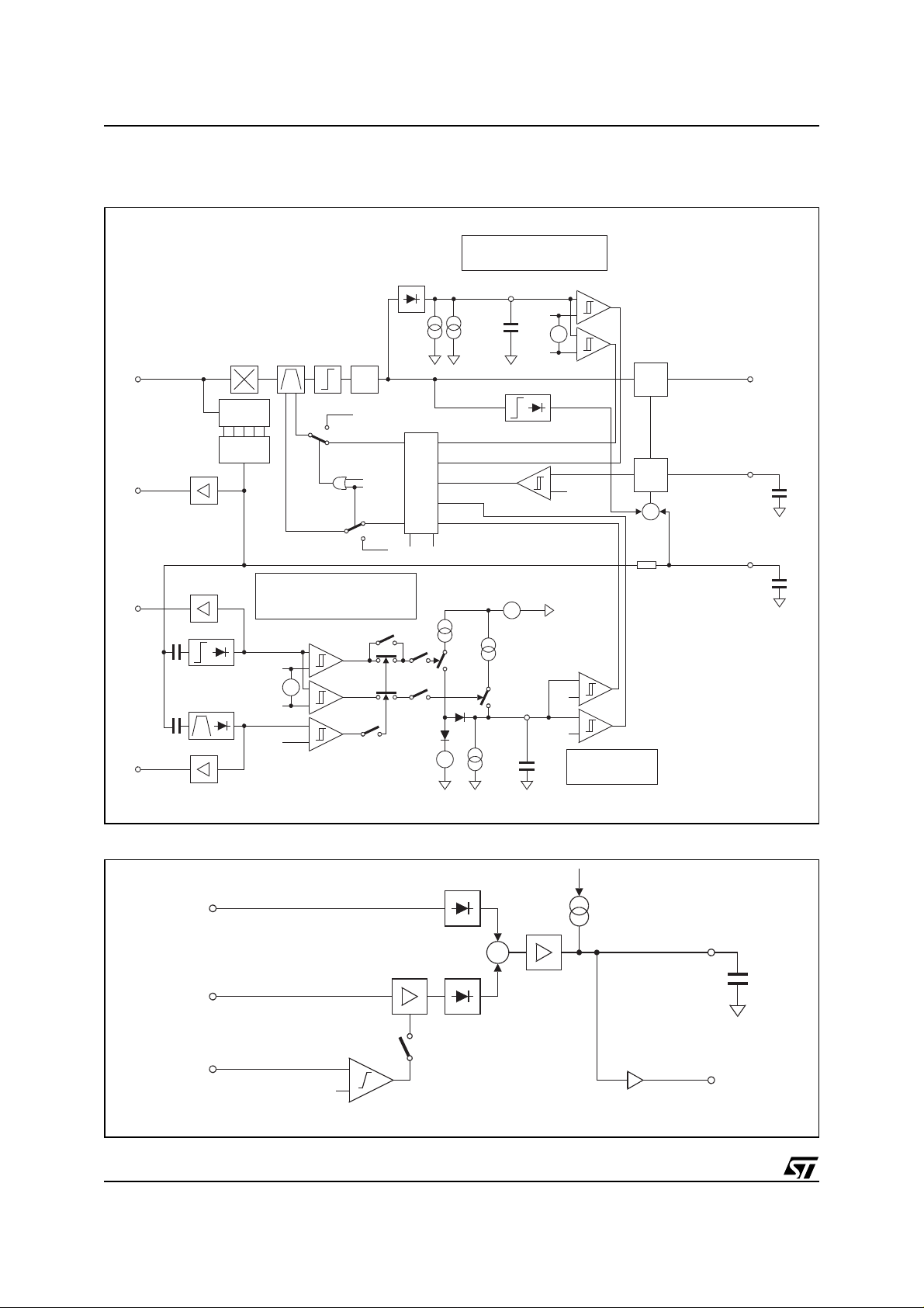
1 FUNCTIONAL DESCRIPTION
1.1 FM Section
1.2 Mixer1, AGC and 1.IF
Mixer1 is a wide dynamic range stage with low noise and large input signal performance. The mixer1 tank can
be adjusted by software (IF1T). The AGC operates on different sensitivities and bandwidths (FMAGC) in order
to improve the input sensitivity and dynamic range (keying AGC). The output signals of AGC are controlled voltage and current for preamplifier and pr estage pin diode attenuator.
Two 10.7MHz programmable amplifier s (IFG1, IFG2) correct the IF ceramic inser tion loss and the cos tumer level plan application.
1.3 Mixer2, Limiter and Demodulator
In this 2. mixer stage the first 10.7MHz IF is converted into the second 450kHz IF. A multi-stage limiter generates
signals for the complete integrated demodulator without external tank. MPX output DC offset compensation is
possible by software (DEM).
(look at Figure 4)
1.4 Quality Detection and ISS
(look at Figure 2)
Fieldstrength
Parallel to mixer2 input a 10.7MHz limiter generates a signal for digital IF counter and a fieldstrength output signal. This internal unweighted fieldstrength is used for keying AGC, adjacent channel and multipath detection
and is available at PIN14 (FSU) after +6dB buffer stage. The behaviour of this output signal can be corrected
for DC offset (SL) and slope (SMSL). The internal generated unweighted fieldstrength is filtered at PIN35 and
used for softmute function and generation of ISS filter switching signal for weak input level (sm).
Adjacent Channel Detector
The input of the adjacent c hannel detecto r is AC c oupled from i nter nal unweighted fiel dstrength. A programmable highpass or bandpass (ACF) and amplifier ( ACG) as well as rectifier determines the influences. This voltage
is compared with adjustable comparator1 thresholds (ACWTH, ACNTH). The output signal of this comparator
generates a DC level at PIN15 by programmable time constant. Time control (TISS) for a present adjacent channel is made by charge and discharge current after comparator1 in an external capacitance. The charge current
is fixed and the discharge current is controlled by I
2
C Bus. This level produces digital signals (ac, ac+) in an
additional comparator4. The adjacent channel information is available as analog output signal after rectifier and
+8dB output buffer.
Multipath Detector
The input of the multipath detector is AC coupled from internal unwe ighted fieldstrength. A programm able bandpass (MPF) and amplifier (MPG) as well as rectifier determines the influences. This voltage is compared with
an adjustable comparator2 thresholds (MPTH). The output signal of this comparator2 is used for the "Milano"
effect. In this case the adjac ent channel detection is switched off. The "Milano" effect is selectable by I
2
C Bus
(MPOFF). The multipath information is available as analog output signal after rectifier and +8dB output buffer.
450kHz IF Narrow Bandpass Filter (ISS filter)
The device gets an additional second IF narrow bandpass filter for suppression nois e and adjacent channel signal influences. This narrow filter has three switchable bandwidthes, narrow range of 80kHz, mid range of
120kHz and 30KHz for weather band information. Without ISS filter the IF bandwidth (wide range) is defined
only by ceramic filter chain. The filter is switched in after mixer2 before 450kHz limiter stage. The centre frequency and matching to the demodulator center frequency can be fine adjusted (AISS) by software..
Deviation Detector
In order to avoid distortion in audio output signal the narrow ISS filter is switched OFF for present overdeviation.
14/41

TDA7511
Hence the demodulator output signal is detected. A lowpass filtering and peak rectifier generates a signal that
is defined by software controll ed current (TDEV) in an external capac itance. This value is c ompared with a programmable comparator3 thresholds (DWTH, DTH) and generates two digital signals (dev, dev+).
ISS Switch Logic
All digital signals coming fr om adjacent channel de tector, devia tion detector and softmute are ac ting vi a sw itching matrix on ISS filter switch. The IF bandpass switch mode is controlled by software (ISSON, ISS30, IS S80,
ISSCTL). The switch ON of the IF bandpass is also available by manipulation of the voltage at PIN15. Two application modes are available (APPM). The conditions are described in table 37.
1.5 Soft Mute Control
The external fieldst reng th signal at PIN 35 is the ref erenc e for mute con trol. The startpoi nt, mute dep th and slop e
are progr ammable (SMTH, SM D, SLOPE) in a w ide range . The time c onstant i s define d by exter nal c apacit ance.
Additional adjacent channel mute function is supported. A highpass filter with -3dB threshold frequency of
100kHz, am plifie r and peak re ctifie r gen erates an adjac ent nois e sign al from MPX outp ut with th e same time co nstant for sof tmute. Thi s value is compare d with compar ator5 thres holds (ACM). For present stron g adjacent cha nnel the MPX signal is attenuated typical 6dB.
1.6 AM Section
The upconversion mixer1 is combined with a gain control circuit 1 sensing three input signals, narrow band information at PIN 39, upconversion signal at PIN 58 and wide band information at PIN 3.This gain control circuit
gives two output signals. The first one is a current for pin diode attenuator and the second one is a voltage for
preamplifier. It is possible to put in a separate narrow bandpass filter before mixer2 at PIN 58. The intervention
point for first AGC (AMAGC) is programmable by software.
The oscillator frequency for mixer1 is generated by dividing the FM V CO frequency (AMD).
In mixer2 the IF1 is downconverted into the IF2 450kHz. Before the output signal reaches the 450kHz tank an
attenuator for IF gain control 2 is passed. Mixer1 and mixer2 tanks are software controlled adjustable
(IF1T, IF2T).
After filtering by ceramic filter a 450kHz amplifier with a gain control 3 is included. The gain control 2 and 3 are
the second AGC and programmable too by s oftware (DAGC). In or der to av oid an osc illation i n intervention point
it is important to know that the D AGC thr eshold has to be smaller than AMAGC! .
The demodulator is a peak detector. A further time constant with capacitor at pin40 produces a DC AGC reference voltage depe ndent on input signal. The ti me c onstant i s s witchable by ratio of 30. This is necessary fo r the
station search function. The switching is software controlled (AMSEEK).
An internal comparator compares the AGC voltage with a programmable reference (AMSS). Consequently it is
possible to generate a seekstop impulse over a defined range.
A separate output is available for AMIF stereo or a permanent seek stop signal(SSTSEL).
1.7 PLL and IF Counter Section
PLL Frequency Synthesizer Block
This part contains a frequency synthesizer and a loop filter for the radio tuning system. Only one VCO is required
to build a complete PLL system for FM and AM upconversion. For auto search stop operation an IF counter
system is available.
The counter works in a two stages configurati on. The first stage is a swallow counter with a two modulus (32/33)
precounter. The second stage is an 11-bit programmable counter.
The circuit receives the sca ling factor s for the progr ammabl e counters and the val ues of the r eference frequencies via an I
2
C-Bus interface.The reference frequency is gener ated by an adjustable internal (XTA L) oscillator
followed by the reference divider. The reference and step-frequencies are free selectable (RC, PC).
Output signals of the phase detector are swi tching the programmable cur rent s ources. The l oop filter i ntegrates
15/41

TDA7511
their currents to a DC voltage.
The values of the current sour ces are programmable by 6 bits also r eceived via the I
To minimize the noise induced by the digital part of the system, a special guard area is implemented.
The loop gain can be set for different conditions by setting the current values of the chargepump generator.
Frequency Generation for Phase Comparison
The RF signals applies a two modulus counter (32/33) pre-scaler, which is controlled by a 5-bit divider(A). The
5-bit register (PC0 to PC4) controls this divider. In parallel the output of the prescaler connects to an 11-bit divider(B). The 11-bit PC register (PC5 to PC15) controls this divider
Dividing range:
f
= (R+1) x f
OSC
f
= [33 x A + (B + 1 - A) x 32] x f
VCO
f
= (32 x B + A + 32) x f
VCO
REF
REF
REF
Important: For correct operation: A ≤ 32; B ≥ A
Three State Phase Comparator
The phase comparator generates a phase error signal according to phase difference between f
This phase error signal drives the charge pump current generator.
Charge Pump Current Generator
This system generators signed pulses of current. The phase error signal decides the duration and polarity of
those pulses. The current absolute values are programmable by A register for high current and B register for
low current.
2
C Bus (A, B, CURRH, LPF).
and f
SYN
REF
.
Inlock Detector
Switching the chargepump in low current mode can be done either via software or automatically by the inlock
detector, by setting bit LDENA to "1".
After reaching a phase difference of 10 - 40nsec and a delay of some times 1/f
in low current mode. A new PLL divider alternation by I
2
C-Bus will switch the chargepump in the high current
, the chargepump is forced
REF
mode.
Few programmable phase errors (D0, D1) are available for inlock detection
The count of detected inlock informations, to release the inlock signal is adjustable (D2, D3), to avoid a switching
to low current during a frequency jump.
Low Noise CMOS Op -a mp
An internal voltage divider at pi n VREF2 connects the positi ve input of th e low n oise op-amp. The c harge pump
output connects the negative input. This inter nal ampli fier in cooperation w ith external components ca n provide
an active filter. The negative input is switchable to three input pins, to increase the flexibility in application. This
feature allows two separate active filters for different applications.
A logical "0" in the LP F register activates PIN LPFM, otherwise PI N LPAM is active. Whil e the high curre nt mode
is activated LPHC is switched on.
IF Counter Block
The input signal for FM and AM upconv ersion is the same 10.7MHz IF level after limiter . The grade of i ntegration
is adjustable by eight different measuring cycle times. The tolerance of the accepted count value is adjustable,
to reach an optimum compromise for search speed and precision of the evaluation.
For the FM range the center frequency of the measured count value is adjustable in 32 steps, to get the possibility of fitting the IF-filter tole rance. In the AM upconversion range an IF frequency of 10.689MHz to 10.720MHz
with 1kHz steps is available.
16/41

TDA7511
The IF -Counter Mode
The IF counter works in 2 modes controlled by IFCM register.
Sampling Timer
A sampling timer to generate the gate signal for the main counter is build wi th a 14-bit programmable counter
(IRC). In FM mode a 6.25kHz, in AM mode a 1kHz basically signal is generated. This is followed by an asynchronous divider to generate several sampling times.
Intermediate Frequency Main Counter
This counter is a 11 - 21-bit synchronous autoreload down counter. Five bits (CF) are programmable to have
the possibility for an adjust to the frequency of the IF-filter . The counter length is automatic adjusted to the chosen sampling time and the counter mode (FM, A M -UPC).
At the start the counter will be loaded with a defined value which is an equivalent to the divider value
(t
SamplexfIF
If a correct frequency is applied to the IF counter frequency input at the end of the sampling time the main
counter is changing its state from 0h to 1FFFFFh.
This is detected by a control logic and an external search stop output is changing from LOW to HIGH. The frequency range inside which a successful count result is adjustable by the EW bits.
).
= (IRC + 1) / f
t
TIM
OSC
t
= (CF + 1697) / f
CNT
= (CF + 10689) / f
t
CNT
IF
IF
FM mode
AM up conversion mode
Counter result succeeded:
t
TIM
t
TIM
≥ t
≤ t
CNT
CNT
- t
+ t
ERR
ERR
Counter result failed:
> t
t
TIM
t
TIM
t
TIM
t
CNT
t
ERR
+ t
CNT
ERR
< t
- t
CNT
ERR
= IF timer cycle time
= IF counter cycle time
= discrimination window (controlled by the EW registers)
The IF counter is only started by inlock information from the PLL part. It is enabled by software (IFENA).
Adjustment of the Measurement Sequence Time
The precision of the measurements is adjustabl e by contr oll ing the disc rimination window. This is adjustabl e by
programming the control registers EW0 to EW2.
The measurement time per cycle is adjustable by setting the Register IFS0 - IFS2.
Adjust of the Frequency Value
The center frequency of the discrimination window is adjustable by the control register CF0 to CF4.
17/41

TDA7511
1.8 I2C-Bus Interface
The TDA 7511 supports the I2C-Bus protocol. This protocol defines any device that sends data onto the bus as
a transmitter, and the receiving device as the receiver. The device that controls the transfer is a master and
device being controlled is the slave. The master will always initiate data transfer and provide the clock to transmit or receive operations.
Data Transition
Data transition on the SDA line must only occur w hen the clock SCL is LOW. S DA transitions while SCL is HIGH
will be interpreted as START or STOP condition.
Start Condition
A start condition is defined by a HIGH to LOW transition of the SDA line while SCL is at a stable HIGH level.
This "START" condition must precede any command and initiate a data transfer onto the bus. The TDA 7511
continuously monitors the SDA and SCL lines for a valid START and will not response to any command if this
condition has not been met.
Stop Condition
A STOP condition is defined by a LOW to HIGH transition of the SDA while the SCL line is at a stable H IGH
level. This condition terminates the communication between the devices and forces the bus-interface of the TDA
7511 into the initial condition.
Acknowledge
Indicates a successful data transfer . The transmitter will release the bus after sending 8 bits of data. During the
9th clock cycle the receiver will pull the SDA line to LOW level to indicate it receive the eight bits of data.
Data Transfer
During data transfer the TDA 7511 samples the SDA line on the leading edge of the SCL clock. Therefore, for
proper device operation the SDA line must be stable during the SCL LOW to HIGH transition.
Device Addressing
To start the communication between two devices, the bus master must initiate a start instructi on sequence, followed by an eight bit word corresponding to the address of the device it is addressing.
The most significant 6 bits of the slave address are the device type identifier.
The TDA 7511 device type is fixed as "110001".
The next significant b it is used to addres s a partic ular devic e of the previ ous defin ed type co nnected to the bus.
The state of the hardw ired PI N 41 defines the s tate of this addr ess bit . So up to two devices could be connected
on the same bus. When PIN 41 is connected to VCC2 the address bit “1” is selected. In this case the AM part
doesn’t work. Otherwise the address bit “0” is selected (FM and AM is working). Therefor a double FM tuner
concept is possible.
The last bit of the start instruction defines the type of operation to be performed:
- When set to "1", a read operation is selected
- When set to "0", a write operation is selected
The TDA 7511 connected to the bus will compare their own hardwired address with the slave address being
transmitted, after detecting a START co ndition. After this comparis on, the TD A 7511 wi ll generate an "acknow ledge" on the SDA line and will do either a read or a write operation according to the state of R/W bit.
18/41
TDA7511
Write Operation
Following a START condition the master s ends a s lave addres s w ord with the R/W bit set to "0". The TDA 7511
will generate an "acknowledge" after this firs t transmission and will wait for a second word (the word addr ess
field). This 8-bit address field provides an access to any of the 32 internal addresses. Upon receipt of the word
address the TDA 7511 slave device will respond with an "acknowledge". At this time, all the following words
transmitted to the TDA 7511 will be considered as Data. The internal address will be automatically in cremented.
After each word receipt the TDA 7511 will answer with an "acknowledge".
Read Operation
IF the master sends a slave address word with the R/W bit set to "1", the TDA 7511 will transit one 8-bit data
word. This data word includes the following informations:
bit0 (ISS filter, 1 = ON, 0 = OFF)
bit1 (ISS filter bandwidth, 1 = 80kHz, 0 = 120kHz)
bit2 (MPOUT,1 = multipath present, 0 = no multipath)
bit3 (1 = P LL is locked in , 0 = PLL is locked out).
bit4 (fieldstrength indicator, 1 = lower as softmute threshold, 0 = higher as softmute threshold)
bit5 (adjacent channel indicator, 1 = adjacent channel present, 0 = no adjacent channel)
bit6 (deviation indicator, 1 = strong overdeviation present, 0 = no strong overdeviation)
bit7 (deviation indicator, 1 = over deviation present, 0 = no overdeviation)
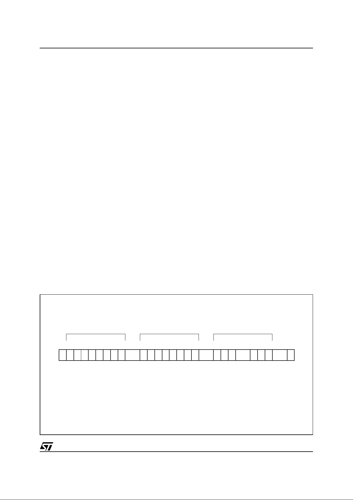
2 Software Specification
The interface protocol comprises:
- start condition (S)
- chip address byte
- subaddress byte
- sequence of data (N bytes + Acknowledge)
- stop condition (P)
Figure 1.
CHIP ADDRESS
MSB LSB
S 1 1 0 0 0 1 0 X
=
Acknowledge
ACK
=
Start
S
=
Stop
P
=
Pagemode
I
=
R/W Bit
X
99AT0054
MSB LSB
ACK T T I A4 A3 A2 A1 A0
SUBADDRESS
DATA1 - DATAn
MSB LSB
ACK DATA
ACK P
19/41

TDA7511
2.1 Address Organ ization
Table 1.
Function Addr 7 6543210
CHARGEPU
MP
LOCKDET 1 LDE NA D3 D2 D1 D0 AMON TEST3 RES2
PLL
COUNTER
PLL REF
COUNTER
TV1 6 TV011 TV010 TVR15 TVR14 TVR13 TVR12 TVR11 TVR10
TV2 7 TV021 TV020 TVR25 TVR24 TVR23 TVR22 TVR21 TVR20
IFC CTRL 1 8 TV013 TV012 TV023 TV022 IFENA EW2 EW1 EW0
IFC CTRL 2 9 IFS2 IFS1 IFS0 CF4 CF3 CF2 CF1 CF0
IF REF CNT1 10 IRC7 IRC6 IRC5 IRC4 IRC3 IRC2 IRC1 IRC0
IF REF CNT2 11 IFCM1 IFCM0 IRC13 IRC12 IRC11 IRC10 IRC9 IRC8
IF1/FMAGC 12 - FMAGC2 FMAGC1 FMAGC0 IFG21 IFG20 IFG11 IFG10
DEM ADJ 13 DNB1 DNB0 DEM5 DEM4 DEM3 DEM2 DEM1 DEM0
QUALITY AC 14 ACNTH1 ACNTH0 ACWTH2 ACWTH1 ACWTH0 ACG ACF ISS30
QUALITY MP 15 MPAC APPM2 APPM1 MPTH1 MPTH0 MPG MPF MPOFF
QUALITYDEV 16 - DTH1 DTH0 DWTH1 DWTH0 TDEV2 TDEV1 TDEV0
QUALITYISS 17 AISS1 AISS0 TISS2 TISS1 TISS0 ISS80 ISSON ISSCTL
AM CTL1 18 DAGC3 DAGC2 DAGC1 DAGC0 AMD1 AMD0 AMST AMSEEK
AM CTL2 19 AMSS3 AMSS2 AMSS1 AMSS0 AMAGC3 AMAGC2 AMAGC1 AMAGC0
MUTE1 20 SMCTH1 SMCTH0 SLOPE MENA SMD3 SMD2 SMD1 SMD0
MUTE2 21 ACM3 ACM2 ACM1 ACM0 SMTH3 SMTH2 SMTH1 SMTH0
SLIDER 22 - - SL5 SL4 SL3 SL2 SL1 SL0
TANK ADJ 23 IF1T3 IF1T2 IF1T1 IF1T0 IF2T3 IF2T2 IF2T1 IF2T0
XTAL ADJ 24 - - CLKSEP XTAL4 XTAL3 XTAL2 XTAL1 XTAL0
TESTCNTRL 25 ISSIN SMSL SSTSEL ISSCOFF DEMOFF 450LOFF TESTOUTTESTIN
0 LPF CURRH B1 B0 A3 A2 A1 A0
2 PC7 PC6 PC5 PC4 PC3 PC2 PC1 PC0
3 PC15 PC1 4 PC13 PC12 PC11 PC10 PC9 PC8
4 RC7 RC6 RC5 RC4 RC3 RC2 RC1 RC0
5 RC15 RC14 RC13 RC12 RC11 RC10 RC9 RC8
TEST 26 - - - - - DIV2 DIV1 DIV0
TEST MODE1 27 OUT7 OUT6 OUT5 OUT4 OUT3 OUT2 OUT1 OUT0
TEST MODE2 28 - - TINMP TINAC OUT11 OUT10 OUT9 OUT8
2.2 Con t rol Re gi s te r Fun c tion
Table 2.
Register Name Function
A Charge pump high current
ACF Adjacent channel filter select
ACG Adjacent channel filter gain
ACM Threshold for startpoint adjacent channel mute
ACNTH Adjacent channel narrow band threshold
ACWTH Ad jacen t channel wide band thres hold
AISS ISS filter fine adjust
20/41

Table 2. (continued)
Register Name Function
AMAGC AM wide band AGC threshold
AMD AM prescaler
AMON AM -FM switch
AMSEEK Switch time constant for AM seek
AMSS AM seek stop threshold
AMST AM stereo select
APPM Application mode quality detection
B Charge pump low current
CF Center frequency IF counter
CLKSEP Clock separation (only for testing)
CURRH Set current high charge pump
D Inlock phase error and delay time for lock detector
DAGC AM narrow band AGC threshold
DEM Demodulator offset
DEMOFF Demodulator clock “OFF” (only for testing)
DNB Demodulator noise blanking
DIV Divider ratio for reference frequency (only for testing)
DTH Deviation detector threshold for ISS filter “OFF”
DWTH Deviation detector threshold for ISS filter narrow/wide
EW Frequency error window IF counter
FMAGC FM AGC threshold
IF1T FM/AM mixer1 tank adjust
IF2T AM mixer2 tank adjust
IFCM IF counter mode
IFENA IF counter enable
IFG IF1 amplifier gain (10.7MHz)
IFS IF counter sampling time
IRC IF reference counter
ISSCOFF ISS filter clock “OFF” (only for testing)
ISSCTL ISS filter control
ISSIN Test input for ISS filter
ISSON ISS filter “ON”
ISS30 ISS filter 30KHz weather band
ISS80 ISS filter narrow/mid switch
LDENA Lock detector enable
LPF Loop filter input select
MENA Softmute enable
MPAC Adjacent channel control by multipath
MPOFF Multipath control “OFF”
MPF Multipath filter frequency
MPG Multipath filter gain
MPTH Multipath threshold
OUT Test output (only for testing)
TDA7511
21/41

TDA7511
Table 2. (continued)
Register Name Function
PC Counter for PLL (VCO frequency)
RC Reference counter PLL
RES Reservation
SL S meter slider threshold
SLOPE Softmute slope select
SMCTH Softmute capacitor threshold for ISS “ON”
SMD Softmute depth threshold
SMSL S mete r slope
SMTH Softmute startpoint threshold
SSTSEL Search stop select for continuous signal
TEST3 Testing PLL/IFC (only for testing)
TESTOUT Switch FSW output to TEST output (only for testing)
TESTIN Switch FSU input to TEST input (only for testing)
TDEV Time constant for deviation detector
TINAC Test input adjacent channel (only for testing)
TINMP Test input multipath(only for testing)
TISS Time constant for ISS filter “ON”/”OFF”
TVR Tuning voltage for prestage proportional referred to PLL
TVO Tuning voltage offset for prestage
XTAL Xtal frequency adjust
450LOFF 450kHz limiter “OFF” (only for testing)
Subaddress
Table 3.
MSB
T2T1 I A4A3A2A1A0
0 0 0 0 0 Charge pump control
0 0 0 0 1 PLL lock detector
------
1 1 1 0 0 Test mode 2
0 Page mode “OFF”
1 Page mode enable
Note: 1. T1, T2 used for testi ng, in application mo de they have to be "0".
LSB
Function
22/41

2.3 Data Byte Specification
Addr 0 Charge Pump Control
Table 4.
TDA7511
MSB
d7 d6 d5 d4 d3 d2 d1 d0
0 0 0 0 High current = 0mA
0 0 0 1 High current = 0.5mA
0 0 1 0 High current = 1mA
0 0 1 1 High current = 1.5mA
-----
1 1 1 1 High current = 7.5mA
00
01
10
11
0 Select low current
1 Select high current
0 Select LPFM
1 Select LPAM
LSB
Low current = 0
Low current = 50
Low current = 100
Low current = 150
Function
µA
µA
µA
µA
Addr 1 PLL Lock Detector
Table 5.
MSB
d7 d6 d5 d4 d3 d2 d1 d0
0 Select FM mode
1 Select AM mode
0 0 PD phase difference threshold 10ns
0 1 20ns
1 0 30ns
1 1 40ns
0 0 Not valid
0 1 Activation delay 4 x 1/f
10 6 x 1/f
11 8 x 1/f
0 Lock detector doesn't control charge pump
1 Lock detector controls charge pump
LSB
0 0 Not used, have to be 0, d1 only for testing
Function
REF
REF
REF
23/41

TDA7511
Addr 2 PLL Counter 1 (LS B)
Table 6.
MSB
LSB
d7 d6 d5 d4 d3 d2 d1 d0
00000000LSB = 0
00000001LSB = 1
00000010LSB = 2
--------11111100LSB = 252
11111101LSB = 253
11111110LSB = 254
11111111LSB = 255
Addr 3 PLL Counter 2 (MSB)
Table 7.
MSB
d7 d6 d5 d4 d3 d2 d1 d0
00000000MSB = 0
00000001MSB = 256
00000010MSB = 512
--------1 1 1 1 1 1 0 0 MSB = 64768
1 1 1 1 1 1 0 1 MSB = 65024
1 1 1 1 1 1 1 0 MSB = 65280
1 1 1 1 1 1 1 1 MSB = 65536
Note: 1. Swallow mode: f
VCO/fSYN
= LSB + MSB + 32
LSB
Function
Function
Addr 4 PLL Reference Counter 1 (LSB)
Table 8.
MSB
d7 d6 d5 d4 d3 d2 d1 d0
00000000LSB = 0
00000001LSB = 1
00000010LSB = 2
--------11111100LSB = 252
11111101LSB = 253
11111110LSB = 254
11111111LSB = 255
24/41
LSB
Function
Addr 5 PLL Reference Counter 2 (MSB)
Table 9.
TDA7511
MSB
d7 d6 d5 d4 d3 d2 d1 d0
LSB
Function
00000000MSB = 0
00000001MSB = 256
00000010MSB = 512
--------1 1 1 1 1 1 0 0 MSB = 64768
1 1 1 1 1 1 0 1 MSB = 65024
1 1 1 1 1 1 1 0 MSB = 65280
1 1 1 1 1 1 1 1 MSB = 65536
Note: 1. f
Addr 6, Addr7, Addr 8 TV1,2 (proportional and offset control referred to tuning voltage V28)
OSC/fREF
= LSB + MSB + 1
Table 10.
addr8 addr6
d7 d6 d7 d6 d5 d4 d3 d2 d1 d 0
addr8 addr7
d5 d4 d7 d6 d5 d4 d3 d2 d1 d 0
000000TVR = 0
000001TVR = -1
000010TVR = -2
------- -011111TVR = -31
100001TVR = +1
100010TVR = +2
----------111111TVR = +31
0000 TVO = 0
0001 TVO = -1
0010 TVO = -2
-----------
0111 TVO = -7
1001 TVO = +1
1010 TVO = +2
----- -----
1111 TVO = +7
Function TV1
Function TV2
Note: 1. TV1,2 = V28 + V28 * TVR/128 + TVO * 50mV
TVR: -31, -30, ... 0 ... 30, 31
TVO: -7, -6, ... 0 ... 6, 7
25/41
TDA7511
Addr 8 IF Counter Control 1
Table 11.
MSB
LSB
d7 d6 d5 d4 d3 d2 d1 d0
000Not valid
001Not valid
010Not valid
011
100
101
110
111
0 IF counter disable / stand by
1 IF counter enable
Addr 9 IF Counter Control 2
Table 12.
MSB
d7 d6 d5 d4 d3 d2 d1 d0
00000f
00001f
--------01010f
01011f
01100f
01101f
01110f
01111f
10000f
10001f
--------11111f
000 t
001 t
010 t
011 t
100 t
101
110
111
LSB
Function
∆f = 6.25kHz (FM)1kHz (AM UPC)
∆f = 12.5kHz (FM) 2kHz (AM UPC)
∆f = 25kHz (FM) 4kHz (AM UPC)
∆f = 50kHz (FM) 8kHz (AM UPC)
∆f = 100kHz (FM)16kHz (AM UPC)
Function
= 10.60625MHz (FM)10.689MHz (AM UPC)
Center
= 10.61250MHz (FM)10.690MHz (AM UPC)
Center
= 10.66875MHz (FM)10.699MHz (AM UPC)
Center
= 10.67500MHz (FM)10.700MHz (AM UPC)
Center
= 10.68125MHz (FM)10.701MHz (AM UPC)
Center
= 10.68750MHz (FM)10.702MHz (AM UPC)
Center
= 10.69375MHz (FM)10.703MHz (AM UPC)
Center
= 10.70000MHz (FM)10.704MHz (AM UPC)
Center
= 10.70625MHz (FM)10.705MHz (AM UPC)
Center
= 10.71250MHz (FM)10.706MHz (AM UPC)
Center
= 10.80000MHz (FM)10.720MHz (AM UPC)
Center
= 20.48ms (FM)128ms (AM UPC)
Sample
= 10.24ms (FM)64ms (AM UPC)
Sample
= 5.12ms (FM)32ms (AM UPC)
Sample
= 2.56ms (FM)16ms (AM UPC)
Sample
= 1.28ms (FM)8ms (AM UPC)
Sample
= 640µs (FM)4ms (AM UPC)
t
Sample
= 320µs (FM)2ms (AM UPC)
t
Sample
t
= 160µs (FM)1ms (AM UPC)
Sample
26/41

Addr 10 IF Counter Reference (LSB)
Table 13.
TDA7511
MSB
d7 d6 d5 d4 d3 d2 d1 d0
LSB
Function
00000000LSB = 0
00000001LSB = 1
00000010LSB = 2
---------
11111100LSB = 252
11111101LSB = 253
11111110LSB = 254
11111111LSB = 255
Addr 11 IF Counter Reference (MSB) and IF Counter Mode Select
Table 14.
MSB
d7 d6 d5 d4 d3 d2 d1 d0
000000MSB = 0
0 0 0 0 0 1 MSB = 256
0 0 0 0 1 0 MSB = 512
------1 1 1 1 0 1 MSB = 15616
1 1 1 1 1 0 MSB = 15872
1 1 1 1 1 1 MSB = 16128
0 0 Not valid
0 1 IF counter FM mode
1 0 Not valid
1 1 IF counter AM upconversion mode
Note: 1. f
OSC/fTIM
= LSB + MSB + 1
LSB
Function
27/41

TDA7511
Addr 12 IF 1 and FM AGC
Table 15.
MSB
LSB
d7 d6 d5 d4 d3 d2 d1 d0
0 0 IF1 gain1 9dB
0 1 IF1 gain1 11dB
1 0 IF1 gain1 13dB
1 1 IF1 gain1 15dB
0 0 IF1 gain2 9dB
0 1 IF1 gain2 11dB
1 0 IF1 gain2 13dB
1 1 IF1 gain2 15dB
000
001
010
011
100
101
110
AGC threshold 80dB
AGC threshold 82dB
AGC threshold 84dB
AGC threshold 86dB
AGC threshold 88dB
AGC threshold 90dB
AGC threshold 92dB
1 1 1 Keying AGC “OFF”
0 has to be “0”
Addr 13 Demodulator Fine Adjust
Table 16.
Function
µV
µV
µV
µV
µV
µV
µV
MSB
LSB
d7 d6 d5 d4 d3 d2 d1 d0
0000000mV
000001+6mV
000010+12mV
------0 1 1 1 1 1 +186mV
1000000mV
100001-6mV
100010-12mV
------1 1 1 1 1 1 -186mV
1 1 have to be “1”
Function
28/41
Addr 14 Quality Detection Adjacent Channel
Table 17.
TDA7511
MSB
d7 d6 d5 d4 d3 d2 d1 d0
0 AC gain 32dB
1 AC gain 38dB
0 0 0 AC wide band threshold 0.25V
0 0 1 AC wide band threshold 0.35V
0 1 0 AC wide band threshold 0.45V
--- -
1 1 1 AC wide band threshold 0.95V
0 0 AC narrow band threshold 0.0V
0 1 AC narrow band threshold 0.1V
1 0 AC narrow band threshold 0.2V
1 1 AC narrow band threshold 0.3V
LSB
1 ISS filter 30KHz “ON”for weather band
0 AC highpass frequency 100kHz
1 AC bandpass frequency 100kHz
Addr 15 Quality Detection Multipath
Table 18.
MSB
d7 d6 d5 d4 d3 d2 d1 d0
0 MP gain 12dB
1 MP gain 23dB
0 0 MP threshold 0.50V
0 1 MP threshold 0.75V
1 0 MP threshold 1.00V
1 1 MP threshold 1.25V
0 0 Application mode 1
0 1 Application mode 2
0 Multipath eliminates ac
1 Multipath eliminates ac and ac+
LSB
0 Multipath control “ON”
1 Multipath control “OFF”
0 MP bandpass frequency 19KHz
1 MP bandpass frequency 31KHz
Function
Function
29/41
TDA7511
Addr 16 Quality Deviation Detection
Table 19.
MSB
LSB
d7 d6 d5 d4 d3 d2 d1 d0
000
001
010
011
charge current 34
charge current 32
charge current 30
charge current 28
µΑ, discharge current 6µΑ
µΑ, discharge current 8µΑ
µΑ, discharge current 10µΑ
µΑ, discharge current 12µΑ
----
111
charge current 20
µΑ, discharge current 20µΑ
0 0 DEV threshold for ISS narrow/wide 30kHz
0 1 DEV threshold for ISS narrow/wide 45kHz
1 0 DEV threshold for ISS narrow/wide 60kHz
1 1 DEV threshold for ISS narrow/wide 75kHz
0 0 DEV threshold for ISS filter “OFF” ratio 1
0 1 DEV threshold for ISS filter “OFF” ratio 1.3
1 0 DEV threshold for ISS filter “OFF” ratio 1.4
1 1 DEV threshold for ISS filter “OFF” ratio 1.5
0 has to be 0
Addr 17 Quality ISS Filter
Table 20.
MSB
d7 d6 d5 d4 d3 d2 d1 d0
0 Switch ISS filter 120kHz
1 Switch ISS filter 80kHz
000
001
010
011
--- -
111
0 0 ISS filter fine adjust -20kHz
0 1 ISS filter fine adjust -10kHz
1 0 ISS filter fine adjust 0kHz
1 1 ISS filter fine adjust +10kHz
LSB
0 ISS filter control “ON”
1 ISS filter control “OFF”
0 Switch ISS filter “OFF”
1 Switch ISS filter “ON”
discharge current1
discharge current3
discharge current5
discharge current7
discharge current15
µA, charge current mid 74µΑ narrow124µΑ
µA, charge current mid 72µΑ narrow122µΑ
µA, charge current mid 70µΑ narrow120µΑ
µA, charge current mid 68µΑ narrow118µΑ
µA,charge current mid 60µΑnarrow110µΑ
Function
Function
30/41
Addr 18 AM Control1
Table 21.
TDA7511
MSB
d7 d6 d5 d4 d3 d2 d1 d0
0 0 Prescaler ratio 10
0 1 Prescaler ratio 8
1 0 Prescaler ratio 6
1 1 Prescaler ratio 4
0000
0001
0010
0011
0100
0101
0110
0111
1000
1001
1010
1011
1100
1101
1110
1111
LSB
0 Multipath information available FM
1 AM stereo output available
Function
0 Normal AGC time constant
1 Short time constant for AM seek stop
Narrow band AGC threshold 74.4dB
Narrow band AGC threshold 78.8dB
Narrow band AGC threshold 80.0dB
Narrow band AGC threshold 80.7dB
Narrow band AGC threshold 53.2dB
Narrow band AGC threshold 77.1dB
Narrow band AGC threshold 78.5dB
Narrow band AGC threshold 79.4dB
Narrow band AGC threshold 42.7dB
Narrow band AGC threshold 65.8dB
Narrow band AGC threshold 77.6dB
Narrow band AGC threshold 78.5dB
Narrow band AGC threshold 32.6dB
Narrow band AGC threshold 55.0dB
Narrow band AGC threshold 73.3dB
Narrow band AGC threshold 77.6dB
µV
µV
µV
µV
µV
µV
µV
µV
µV
µV
µV
µV
µV
µV
µV
µV
Addr 19 AM Control2
Table 22.
MSB
d7 d6 d5 d4 d3 d2 d1 d0
0000
0001
0010
0011
0100
0101
0110
0111
1000
1001
1010
LSB
AGC Threshold 82.0dB
AGC Threshold 85.4dB
AGC Threshold 87.5dB
AGC Threshold 89.2dB
AGC Threshold 90.6dB
AGC Threshold 91.9dB
AGC Threshold 92.9dB
AGC Threshold 93.8dB
AGC Threshold 94.6dB
AGC Threshold 95.4dB
AGC Threshold 96.1dB
Function
µV 80.1dBµV
µV 83.4dBµV
µV 85.5dBµV
µV 87.2dBµV
µV 88.6dBµV
µV 89.8dBµV
µV 90.8dBµV
µV 91.8dBµV
µV 92.6dBµV
µV 93.3dBµV
µV 94.0dBµV
31/41

TDA7511
Table 22. (continued)
MSB
d7 d6 d5 d4 d3 d2 d1 d0
1011
1100
1101
1110
1111
0000
0001
0010
0011
0100
0101
0110
0111
1000
1001
1010
1011
1100
1101
1110
1111
LSB
AGC Threshold 96.7dB
AGC Threshold 97.3dB
AGC Threshold 97.8dB
AGC Threshold 98.4dB
AGC Threshold 98.8dB
Seek stop threshold 20.3dB
Seek stop threshold 20.8dB
Seek stop threshold 21.3dB
Seek stop threshold 22.0dB
Seek stop threshold 22.8dB
Seek stop threshold 23.7dB
Seek stop threshold 24.7dB
Seek stop threshold 25.9dB
Seek stop threshold 27.0dB
Seek stop threshold 28.6dB
Seek stop threshold 30.4dB
Seek stop threshold 32.5dB
Seek stop threshold 35.2dB
Seek stop threshold 37.6dB
Seek stop threshold 40.2dB
Seek stop threshold 43.0dB
µV 94.6dBµV
µV 95.2dBµV
µV 95.7dBµV
µV 96.3dBµV
µV 96.8dBµV
Function
µV
µV
µV
µV
µV
µV
µV
µV
µV
µV
µV
µV
µV
µV
µV
µV
Addr 20 S oftmute Cont rol 1
Table 23.
MSB
d7 d6 d5 d4 d3 d2 d1 d0
0 0 0 0 Mute depth 0 in application 18dB
0 0 0 1 Mute depth 1 in application 20dB
0 0 1 0 Mute depth 2 in application 22dB
0 0 1 1 Mute depth 3 in application 24dB
- - - - - (logarithmically behaviour)
1 1 1 1 Mute depth 15 in application 36dB
0 Mute disable
1 Mute enable
0 Sharp slope
1 Smooth slope
0 0 Function “OFF”
0 1 Mute depth threshold for ISS filter “ON” 2dB
1 0 Mute depth threshold for ISS filter “ON” 1dB
1 1 Mute depth threshold for ISS filter “ON” 0.2dB
LSB
Function
32/41

Addr 21 S oftmute Cont rol 2
Table 24.
TDA7511
MSB
LSB
d7 d6 d5 d4 d3 d2 d1 d0
0000
0001
0010
0100
Startpoint mute 0 in application 3dB
Startpoint mute 1 in application 4dB
Startpoint mute 2 in application 5dB
Startpoint mute 3 in application 6dB
----1111
Startpoint mute 15 in application 18dB
0 0 0 0 AC mute threshold 60mV
0 0 0 1 AC mute threshold 80mV
0 0 1 1 AC mute threshold 100mV
---0 1 0 0 0 AC mute threshold 220mV
1 1 1 1 AC mute “OFF”
Addr 22 S-Meter Slider
Table 25.
MSB
d7 d6 d5 d4 d3 d2 d1 d0
0 0 0 0 0 0 S meter offset 0mV
0 0 0 0 0 1 S meter offset -58mV
0 0 0 0 1 0 S meter offset -116mV
------0 1 1 1 1 1 S meter offset -1798mV
1 0 0 0 0 0 S meter offset 0mV
1 0 0 0 0 1 S meter offset +58mV
1 0 0 0 1 0 S meter offset +116mV
------1 1 1 1 1 1 S meter offset +1798mV
x x Not used
LSB
Function
µV
µV
µV
µV
µV
Function
33/41

TDA7511
Addr 23 Tank Adjust
Table 26.
MSB
LSB
d7 d6 d5 d4 d3 d2 d1 d0
0 0 0 0 450kHz 0pF
0 0 0 1 450kHz 1.6pF
0 0 1 0 450kHz 3.2pF
0 0 1 1 450kHz 4.8pF
-----
1 1 1 1 450kHz 24pF
0 0 0 0 10.7MHz 0pF
0 0 0 1 10.7MHz 0.55pF
0 0 1 0 10.7MHz 1.1pF
0 0 1 1 10.7MHz 1.65pF
---- -
1 1 1 1 10.7MHz 8.25pF
Addr 24 XTAL Adjust
Table 27.
MSB
d7 d6 d5 d4 d3 d2 d1 d0
00000C
00001C
00010C
00011C
00100C
------
11111C
0 Only for testing has to be “0”
x x Not used
LSB
Load
Load
Load
Load
Load
Load
0pF
0.625pF
1.25pF
1.875pF
2.5pF
19.4pF
Function
Function
Addr 25 Test Control
Table 28.
MSB
d7 d6 d5 d4 d3 d2 d1 d0
0 0 0 0 0 Only for testing (bits have to be “0”)
0 AMIF select
1 Permanent search stop select for AM
0 S meter slope 1V/decade
1 S meter slope 1.5V/decade
0 Only for testing (has to be “0”)
34/41
LSB
Function

Addr 26 Test
Table 29.
TDA7511
MSB
d7 d6 d5 d4 d3 d2 d1 d0
LSB
Function
x x x x x 1 1 0 Only for testing (bits have to be set)
Addr 27 Test Mode1
Table 30.
MSB
d7 d6 d5 d4 d3 d2 d1 d0
0 0 0 0 0 0 0 0 Only for testing (bits have to be set)
Addr 28 Test Mode2
LSB
Function
Table 31.
MSB
d7 d6 d5 d4 d3 d2 d1 d0
x x 0 0 0 0 0 0 Only for testing (bits have to be set)
LSB
Function
35/41
TDA7511
APPENDIX
Figure 2.
Pin46
FMMIX2IN1
Pin14
FSU
Pin13
ADJCH
Pin34
AMST/MP
00AT0006
10.7 MHz
S-Meter
AC Detector
MP Detector
ISS
Limiter
ACWTH < AC
ACWTH + ACNTH < AC
MPTH < MP
AC
ACWTH
+
ACNTH
MP
MPTH
DEV
+
33nF
1
1
+
4V
2V
DEV+
0
1
+
-
+
-
SMCTH
+
-
+
-
V15 > 2V
V15 > 4V
MUTE
MUTE
TC
Attack current 50µA
Decay current 2.5µA
+
12kΩ
- All switches are drawn for function "OFF"
- Software explanation:
16<7> Means address 16 and data d7
AC
AC+
1
0
1
1
Pin37
MPX/AFAM
Pin42
MUTETC
Pin35
FSW
V20 > DWTH
max 40µA
5µA
MPX
DEM
17<2>
Int80 dev
16<7>
Logic
17<1>
Inton
High
15<5> 15<6>
Y1
Y2
Y3
1
0
x
1
1
x
x
x
1
16<7>
+
Y1
-
+
Y2
-
+
Y3
-
15<0>
17<0>
2.5V
V20 > DTH + DWTH
DC 3V
1...15µA
TDEV
dev+
sm
ac
ac+
50µA
1...15µA
+
-
TISS
DEVTC
Pin20
AC MUTE
Detector
5V
-
+
75µA
ISSTC
Pin15
DWTH
DTH
Figure 3.
36/41
FMRFAGCIN
Pin11
80dBu
FMIFAGCIN
Pin11
82...92dBu
Internal
Unweighted
Fieldstrength
00AT0007
Wide
Band
Range
Mid
Band
Range
Narrow
Band
Range
FMAGC
12.5µA
+
0...10dB
I
max 1.25mA
Sink
Keying AGC off
(= 0dB)
+
-
FMMOSDR
Pin6
FMPINDR
Pin5
TDA7511
Block Diagram Quality Detection Principle
Table 32.
Signal LOW HIGH
ac No adjacent channel Adjacent channel present
ac+ No strong adjacent channel Adjacent channel higher as ac
sm Fieldstrength higher as softmute threshold Fieldstrength lower as softmute threshold
dev Deviation lower as threshold DWTH Deviation higher as threshold DWTH
dev+ Deviation lower as threshold DTH*DWTH Deviation higher as threshold DTH*DWTH
inton ISS filter off by logic (wide) ISS filter on by logic
int80 ISS filter 120kHz (mid) ISS filter 80kHz (narrow)
Table 33.
Input Signals Mode1 Mode2
ac ac+ sm dev dev+ inton int80 Function inton int80 Function
0000000wide00wide
0001000wide00wide
0001100wide00wide
0 0 1 0 0 1 1 narrow 1 1 narrow
0011000wide10mid
0011100wide00wide
1 0 0 0 0 1 1 narrow 1 0 mid
1 1 0 0 0 1 1 narrow 1 1 narrow
1001010mid10mid
1 1 0 1 1 1 0 mid 1 1 narrow
1 0 1 0 0 1 1 narrow 1 1 narrow
1 1 1 0 0 1 1 narrow 1 1 narrow
1011010mid10mid
1 1 1 1 0 1 0 mid 1 1 narrow
1011110mid10mid
1 1 1 1 1 1 0 mid 1 1 narrow
Part List (App li ca ti on- and Measurm ent Circuit)
Table 34.
Item Description
F1 TOKO 7KL 600ENS-9132NK
F2 TOKO 7KL 600ENS-9390AQ
F3 TOKO 7KL V600ENS-9469BS
F4 TOKO 7PSG 628AC-5022N
F5 TOKO PGL 5PGLC-5103N
L1,L5 SIEMENS SIMID03 B82432 1mH
L2,L4 TOKO FSLU 2520-680 68µH
L3 TOKO FSLU 2520-150 15µH
CF1,CF2 MURATA SFE10.7MS3A10-A 180KHz or (TOKO CFSK107M3-AE-20X)
CF3 MURATA SFE10.7MJA10-A 150KHz or (TOKO CFSK107M4-AE-20X)
CF4 MURATA SFPS 450H 6KHz or (TOKO ARLFC450T)
T1,T2 COMPONEX B4F 617PT-1026
D1,D3,D5 TOKO KV1410
D2,D4 TOSHIBA 1SV172
Q1 TOSHIBA 3SK126
Q2 TOSHIBA HN3G01J
37/41
TDA7511
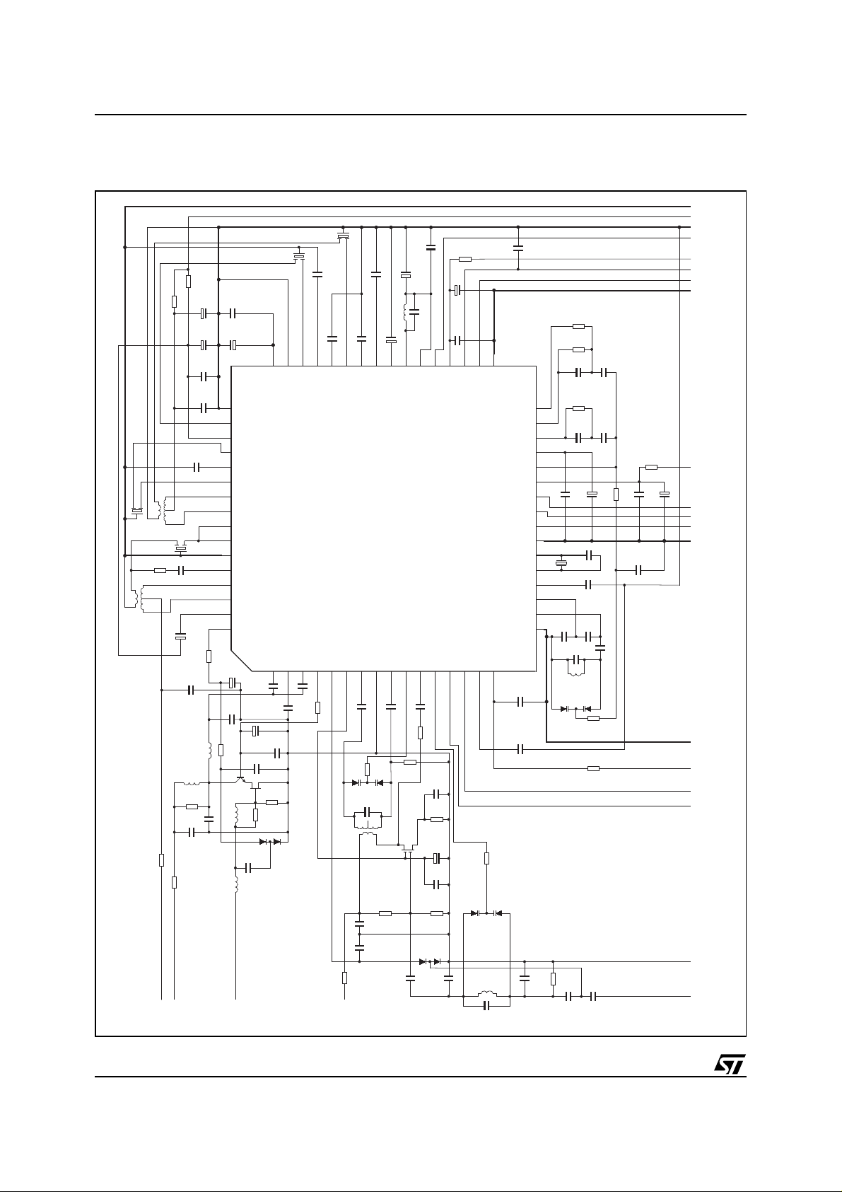
3 APPLICATION CIRCUI
Figure 4.
R
14
4.7Ω
R
C
CF2
5
4
F4
99AT0056
1
2
3
R
27Ω
13
5
4
F5
R
33
12kΩ
V
CCIFVCCAM
15
4.7
Ω
1
2
3
C
100nF
R
12
27Ω
C
22nF
CF1
C
58
100pF
C
1µF
2.2kΩ
9
L1
1mH
R
11
1kΩ
68pF
C
12
100nF
7
L2
68µH
22µF
C
47µF
C
19
100nF
C
18
100nF
17
R
C
C
21
60
100nF
C
20
22
22µF
49
GNDVCC2
50
FMAMP2OUT
51
VCC2
52
FMAMP2IN1
53
FMIF1REF
54
FMAMP1OUT
55
AMMIX2OUT2
56
AMMIX2OUT1
57
FMAMP1IN
58
AMIF1IN
59
GNDIF1AMP
60
FMIFAGCIN
61
MIX1OUT2
62
MIX1OUT1
63
AMRFAGCTC
64
AMPINDR
9
C6
2.2µF
C
36
22nF
C
13
100pF
C
10
2.2
1µF
Ω
k
330nF
Q2
R
910kΩ
L4
R
3
68
5
10kΩ
µH
C
3
4.7nF
L3
15
µH
AMANT
CF3
48
VREF1
AMMIX1IN2
1
C
35
22nF
C
11
10nF
10
D4
1SV172
SPTS450
4647
GNDDEM
FMMIX2IN1
AMMIX1IN1
AMRFAGCIN
3
2
22
C
37
nF
R
4.7kΩ
CF4
C
22nF
C
26
470
nF
FMMIX2IN2
AMRFAGCOUT
4
8
24
4445
FMDEMC
FMPINDR
5
V
C
25
470
nF
43
AMIF2IN
FMMOSDR
6
C
65
5.6
pF
C
33
3.3pF
1
F2
R
29
27Ω
CCFM
C
32
3.9
nF
C
27
10
µF
AMDETC
MUTE TC
TDA 7511
FMMIX1IN1
GNDRF
78
C
66
5.6
pF
R
23
56kΩ
D3
KV1410
2
3
54
R
28
100kΩ
C
50
100nF
C
1
10nF
L5
1
mH
AMAGC2TC
FMMIX1IN29TV1
R
56kΩ
C
31
10pF
C
10nF
C
28
22µF
39404142 38
AMIFBPP
10 11
C
67
10
pF
25
Q1
29
C
61
120
pF
AMIFREF
FMRFAGCIN
R1
1k
Ω
C
10nF
R
330Ω
C
10nF
R
100kΩ
D2
1SV172
C
3.3pF
GNDIFAMP
VCC2
GNDVCC2
R
16
100Ω
C
31
47
µF
C
30
100
nF
3435
3637
FSW
VCC1
ADJCH
13 14
FSU
AMST/MP
ISSTC
15 16
MPX/AFAM
TV2
12
26
26
C
49
1µF
2
27
33
GNDVCC1
VCCVCO
R
30
56kΩ
D1
KV1410
LPHC
LPFM
LPAM
VREF2
LPOUT
VCC3
SCL
SDA
SSTOP
GNDVCC3
XTALG
XTALD
DEVTC
VCOE
VCOB
GNDVCO
C
47
100nF
C
67
33nF
100nF
R
19
8.2kΩ
R
18
56kΩ
C
C
35
36
1nF
6.8nF
R
17
100kΩ
32
31
30
29
28
27
26
25
C
100
nF
C
2.2nF
37
C
34
33
10nF
R
10Ω
C
40
47
µF
C
R
20
100
680
nF
Ω
24
23
C
C
68pF
X
C
12.25
MHz
1
C
42
22nF*
C
45
16
15pF
C
43
3.3pF
41
6.8nF
C
44
22
pF
22
X1
21
20
19
18
17
45
F3
KV1410
R
21
5.6kΩ
R
22
10Ω
MPX/AFAM
VCC1
FSW
AMST-MP
GNDVCC1
32
VCC3
C
38
39
10
µF
SCL
SDA
SSTOP
GNDVCC3
GNDVCO
VCCVCO
FSU
ADJCH
RFGND
C
R
53
F1
45
C
14
3pF
47pF
54
31
C
15
56kΩ
C
47pF
120pF
33
FMANT
38/41

4 MEASUREMENT CIRCUIT
Figure 5.
TDA7511
R
23
4.7Ω
C
6
22µF
C
2
100nF
R
22
4.7Ω
C
5
47µF
C
1
100nF
SFE10.7
R
6
27Ω
T2
617PT1026
CF3
SFE10.7
MJA10
C
39
22nF
CF2
MS3
CF1
SFE10.7MS3
C
100pF
37
4
6
C
100nF
40
F5
45
321
49
50
51
52
53
54
55
56
57
58
59
R
14
60
Ω
12k
61
1
2
62
3
63
C
45
1µF
64
C
100nF
C
22µF
GNDVCC2
FMAMP2OUT
VCC2
FMAMP2IN1
FMIF1REF
FMAMP1OUT
AMMIX2OUT2
AMMIX2OUT1
FMAMP1IN2
AMIF1IN
GNDIFAMP
FMIFAGCIN
MIX1OUT2
MIX1OUT1
AMRFAGCTC
AMPINDR
C
10nF
PJ1
3
7
21
VREF1
GNDDEM
AMMIX1IN2
AMMIX1IN1
2 3 4 5 6 7 8 9 101112131415161
C
20
10nF
R
2
50Ω
BNC
AM-RFIN
C
22nF
FMMIX2IN1
FMMIX2IN2
AMRFAGCIN
AMRFAGCOUT
C
13
R
1nF
4.7kΩ
SFPS450H
4
FMDEMC
FMPINDR
9
CF4
C
11
470
nF
AMIF2IN
MUTETC
FMMOSDR
FMMIX1IN1
R
91Ω
123
T1
64
PJ2
C
15
1µF
R
1
4.7kΩ
22mF
C
10
3.9nF
C
9
470
nF
AMDETC
TDA 7511
GNDRF
12
C
19
1nF
BNC
FM-RFin
C
63
L5
1mH
C
10
µF
AMAGC2TC
FMMIX1IN2
R
91Ω
617PT-1026
12
11
C
36
1nF
C
10nF
C
57
120
pF
39404142 38
AMIFBPP
TV1
PJ3
58
AMIFREF
FMRFAGCIN
50Ω
BNC
FMRFAGCIN
P12 P13 P14
FSW
MPX/AF
R
15
100Ω
VCC1
MPX/AFAM
TV2
ADJCH
C
53
1nF
R
3
FSW
FSU
AMst/MP
100nF
C
42
47µF
C
32
100nF
AMST/MP
SWBPFTC
C
53
33nF*
3334353637434445464748
GNDVCC1
VCCVCO
LPHC
LPFM
LPAM
VREF2
LPOUT
VCC3
SSTOP
GNDVCC3
XTALG
XTALD
DEVTC
VCOE
VCOB
GNDVCO
P16
VCC
P17
R
17
8.2kΩ
R
18
56kΩ
32
C
43
1nF
31
R
100kΩ
30
C
23
2.2nF
29
28
27
26
SCL
25
SDA
24
C
C
29
41
6.8nF
C
10nF
47µF
C
22
31
10nF
C
C
33
30
100nF
10µF
R
19
47Ω
SCL
SDA
P9
SSTOP
16
23
R
22
21
20
19
18
17
22nF*
X1
10.25MHz
C
28
C
24
15pF
C
27
22pF
C
34
100nF
R
20
680Ω
C
35
6.8nF
R
21
5.6kΩ
C
25
D5
68pF
KV1410
C
26
3.3pF
46
F3
600ENS_9469N
13
10Ω
P2
99AT0057
AM-RF-AGCOUT
FM-MOS Driver
AM-PIN Driver
FM-PIN Driver
P1 P3 P4 P5 P6 P7 P8
Tuning V oltage 1
Tuning V oltage 2
Adjacent Channel OUT
Unweighted Fieldstrength
VCCVCO
P15
39/41
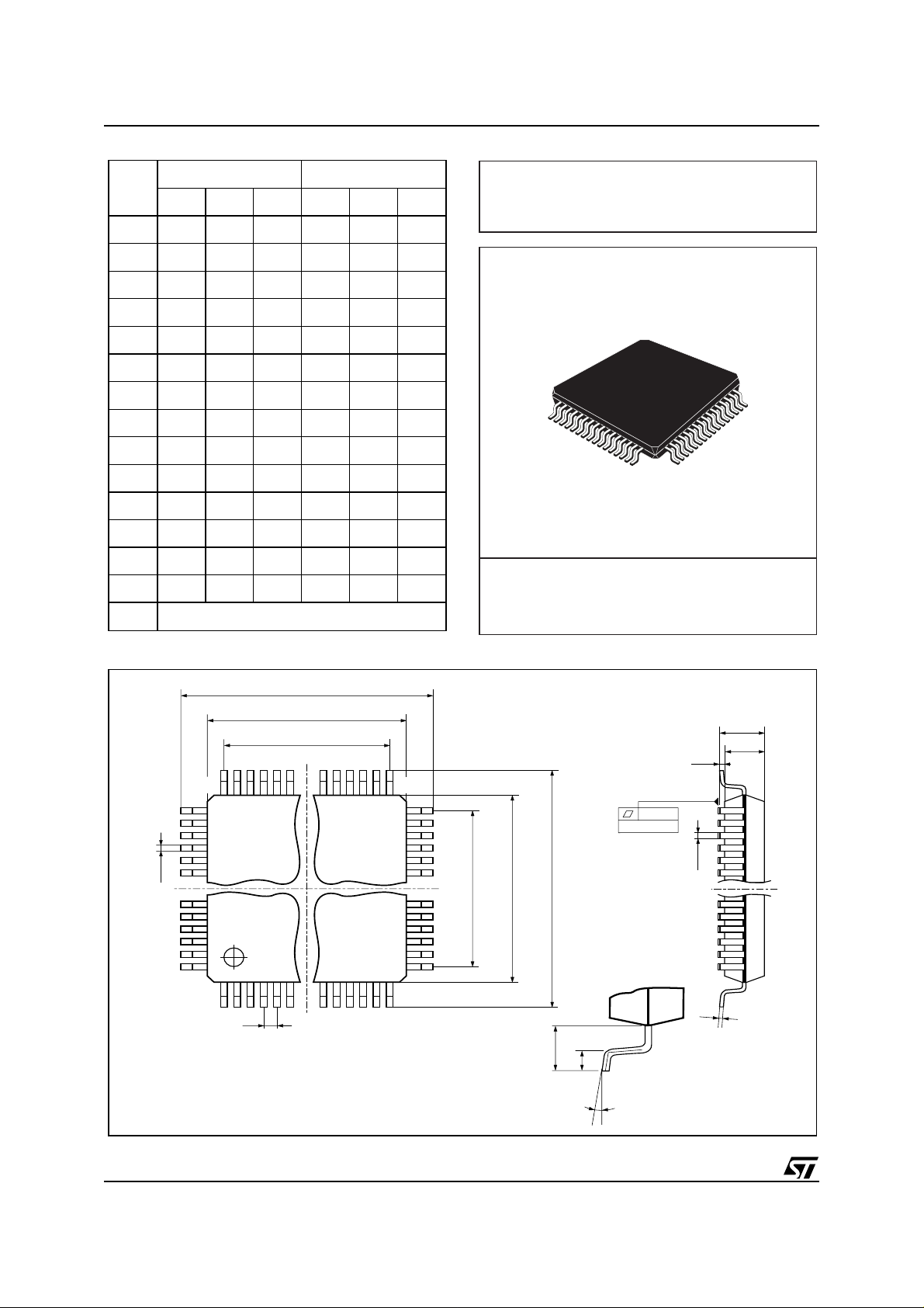
TDA7511
DIM.
mm inch
MIN. TYP. MAX. MIN. TYP. MAX.
A 1.60 0.063
A1 0.05 0.15 0.002 0.006
A2 1.35 1.40 1.45 0.053 0.055 0.057
B 0.18 0.23 0.28 0.007 0.009 0.011
C 0.12 0.16 0.20 0.0047 0.0063 0.0079
D 12.00 0.472
D1 10.00 0.394
D3 7.50 0.295
e 0.50 0.0197
E 12.00 0.472
E1 10.00 0.394
E3 7.50 0.295
L 0.40 0.60 0.75 0.0157 0.0236 0.0295
L1 1.00 0.0393
K 0°(min.), 7°(max.)
OUTLINE AND
MECHANICAL DATA
TQFP64
D
D1
TQFP64
3348
32
E3D3E1
17
16
E
L1
L
0.10mm
Seating Plane
K
49
B
64
1
e
A1
B
A
A2
C
40/41

TDA7511
Information furnished is believed to be accurate and reliable. However, STMicroelectronics assumes no responsibility for the consequences
of use of such information nor for any infringement of patents or other rights of third parties which may result from its use. No license is granted
by implic ation or otherwise under any patent or patent r i ght s of STMi croelectr oni cs. Spec i fications mentioned i n this publication are subject
to change without notice. This publication supersedes and replaces all information previously supplied. STMicroelectronics product s are not
authorized for use as cri tical comp onents in lif e support devi ces or systems without express written approva l of STMicroel ectronics.
The ST logo is a registered trademark of STMicroelectronics
2001 STMicroelectronics - All Ri ghts Rese rved
Austra lia - Brazil - Canada - Chi na - F i nl and - Franc e - Germany - Hong Kong - In di a - Israel - Ita l y - J apan -Malaysia - Malta - Morocco -
Singap ore - Spain - Sw eden - Switze rl and - Unit ed K i ngdom - United States .
STMicroelectronics GROUP OF COMPANIES
http://www.s t. com
41/41
 Loading...