

IN-CAR REMOTE AMPLIFIER DSP
24-Bit Fixed-point DSP core delivering up to
50 MIPS
2x512 x 24BitofRAMforX andYdatamemory.
1536 x 24 Bitof RAMfor Program.
1536 x 24 Bit of Additional RAM memory us-
able fordelay or program
SerialAudio Interface.
DebugPort.
Control Interface for external GPIOs, Inter-
rupts,and RESET.
SPI andI
nal micro andDSP. Both master and slaveoperating modes.
PLL Clock Oscillator
5V-tolerant3V I/O interface
DESCRIPTION
This device is a high-performance,fully programmable DSP, suitable for a wide range of applications and particularly for Audio and Sound Processing. It contains a 24-bit 50 MIPS DSP core,
several interfaces for control and data, plus a
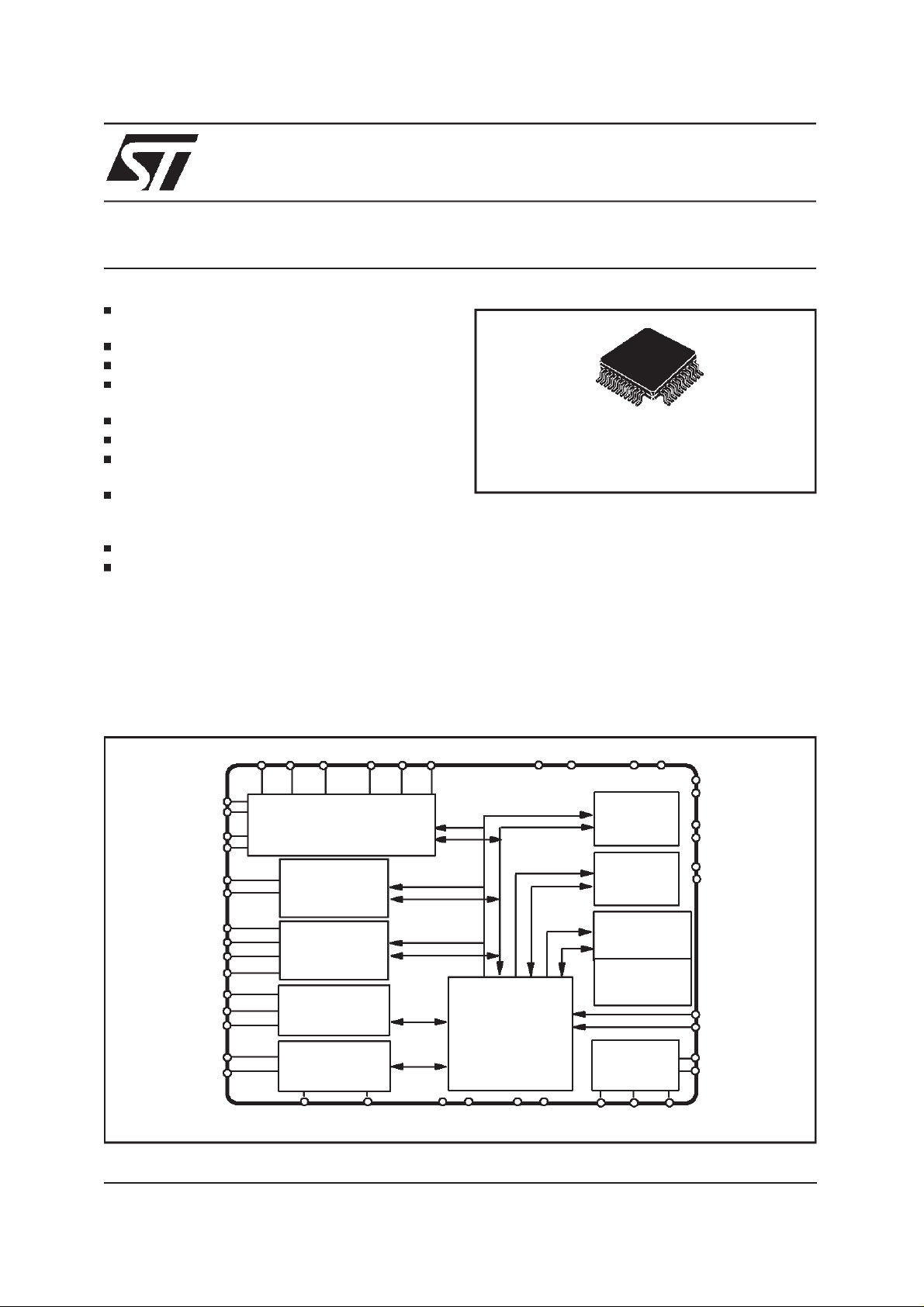
BLOCK DIAGRAM
2
C for communicationbetween exter-
TDA7502
PRODUCT PREVIEW
TQFP44
(10 x 10)
configurablePLL.
The computational power and the memory con-
figuration make this device particularly suitable
for in car equalisation. This device will offer the
best trade-off between performance and cost
when coupled with the TDA7531, or other devices of the same family.A library of sound processing functions is available for this device; some
of these functions are: parametric equaliser,
cross over filters, acoustic delay, dynamic compression, Vol/Bass/Treble/Fader, active equalisation, StereoSpatial Enhancement.
SDI0 SDI1 SDI2 SDO0 SDO1 SDO2 VDD3 GND3 SCANEN TESTEN
LRCLKT
SCKT
LRCLKR
SCKR
SCL
SDA
SS
SCK
MISO
MOSI
GPIO3
GPIO4
GPIO5
DBCK/GPIO1
DBIN/GPIO2
DBRQN/GPIO3 DBRQ VDD1 GND1 VDD2 GND2 XTO XTI CLKOUT
April 1999
This is preliminary information on a new product foreseen to be developed. Details are subject tochange withoutnotice.
Serial
Audio
Interface
I2C
Interface
SPI
Interface
GPIO
Debug
interface
XAB
XDB
YAB
YDB
PAB
ORPHEUS
24bit DSP
CORE
PDB
512 x 24
X-RAM
512 x 24
Y-RAM
3072 x 24
P/Delay-RAM
128 x 24
BOOT-ROM
PLL
oscillator
VDD4
GND4
VDD5
GND5
VDD6
GND6
RESET
INT
PVCC
PGND
1/8
TDA7502
ABSOLUTE MAXIMUM RATINGS
Symbol Parameter Value Unit
V
DDC
V
DDP
V
I,VIN
T
op
T
stg
PIN CONNECTION
Core DC Supply voltage 4.6 V
Pads DC Supply voltage 4.6 V
Digital or analog input voltage -0.5 to (VDDP +0.5) V
Operative temperature range -40 to 85 °C
Storage temperature range (plastic) -55 to 150 °C
SDI0
SDA
3435363738394041424344
SDI1
SCL
33
32
31
30
29
28
27
26
25
24
23
SDI2
SCKT
LRCKT
GND5
VDD5
SDO2
SDO1
SDO0
GND4
VDD4
SCKR
LRCKR
VDD1
GND1
INT
SCANEN
TESTEN
DBRQN
DBOUT
VDD2
GND2
DBCK
DBIN
GND6
VDD6
XTI
XTO
MISO
MOSISSSCK
VDD3
RESET
GND3
GPIO3
GPIO5
GPIO4
1
2
3
4
5
6
7
8
9
10
11
12 13 14 15 16 17 18 19 20 21 22
PVCC
PGND
CLKOUT
THERMAL DATA
Symbol Parameter Value Unit
th j-amb Thermal Resistance Junction to Ambient 50 °C/W
R
PIN DESCRIPTION
N. Name Type
1 VDD1 I – 3.3V core supply.
2 GND1 I – Core ground.
3 INT I/O – External interrupt line (Input/Output). When this line is asserted low, the
4 SCANEN I – SCAN Enable When active with TESTEN also active, controls the
5 TESTEN I – Test Enable. When active, puts the chip into test mode and muxes the
6 DBRQN I – Debug Port Request Input. Means of entering the Debug mode of
2/8
Reset
Status (1)
Function
DSP may be interrupted. Acts as IRQA line of DSP core.
shifting of the internal scan chains.
XTI clock to all flip-flops. When SCANEN is also active, the scan chain
shifting
operation.
PIN DESCRIPTION(continued)
TDA7502
N. Name Type
Reset
Status
Function
7 DBOUT/GPIO2 I/O I The serial data output for the Debug Port. Can also be used as a GPIO.
8 VDD2 I – 3.3V core supply.
9 GND2 I – Core ground.
10 DBCK/GPIO0 I/O I Debug Port Bit Clock/Chip Status 1. The serial clock for the Debug Port
is provided when an input. When an output, provides information about
the chip status. Can also be used as GPIO
11 DBIN/GPIO1 I/O I Debug Port Serial Input/Chip Status 0. The serial data input for the
Debug Port is provided when an input. When an output, provides
information about the chip status. Can also be used as GPIO.
12 CLKOUT O – Output Clock.
13 PGND I – PLL Clock Ground Input. Ground connection for oscillator circuit.
14 PVCC I – PLL Clock Power Supply. Positive supply for PLL Clock Oscillator.
15 XTO O High Crystal Oscillator Output. Crystal Oscillator output drive.
16 XTI I – Crystal Oscillator Input. External Clock Input or crystal connection.
17 RESET I/O I System Reset. A logic low level applied to RESET input initializes DSPs.
During Debug Mode if this pin is pulled low in while the DBRQN line is
pulled low then the DSP pointed to by the DBSEL pin will be reset.
18 VDD3 I – 3.3V Supply.
19 GND3 I – Ground.
20 SDI0 I – SDI0 is a stereodigital audio data inputpin channel0.
21 SDI1 I – SDI1 is a stereodigital audio data inputpin channel1.
22 SDI2 I – SDI2 is a stereodigital audio data inputpin channel2.
23 SCKR I/O – SAI receive bit clock. Master or slave.
24 LRCKR I/O – Left-Right clock for SAI Receiver. Master or slave.
25 VDD4 I – 3.3V Supply.
26 GND4 I – Ground.
27 SDO0 O High SDO0isa stereodigital audiodataoutputpinchannel 0.
28 SDO1 O High SDO1isa stereodigital audiodataoutputpinchannel 1.
29 SDO2 O High SDO2isa stereodigital audiodatapin channel2.
30 VDD5 GND – 3.3V Supply.
31 GND5 I – Ground.
32 LRCKT I/O – SAI transmit left/right clock. Master or slave.
33 SCKT I/O – SAI transmit bit clock. Master or slave.
34 SCL I/O – Clock line for I
35 SDA I/O – Data line for I
2
C bus. Schmitt trigger input.
2
C bus. Schmitt trigger input.
36 SCK I – Bit clock for SPI control interface.
37 SS I – Slave select input pin for SPI control interface.
38 MOSI I/O I Serial Data Output for SPI type serial port when in SPI Master Mode and
Serial Data Input when in SPI Slave Mode.
39 MISO I/O I Serial Data Input for SPI style serial port when in SPI Master Mode and
Serial Data Output when inSPI Slave Mode.
40 VDD6 GND – 3.3V Supply.
41 GND6 I – Ground.
42 GPIO3 I/O – This pin is dedicated as general I/O.
43 GPIO4 I/O – This pin is dedicated as general I/O.
44 GPIO5 I/O – This pin is dedicated as general I/O.
3/8

TDA7502
RECOMMENDED DC OPERATING CONDITIONS
Symbol Parameter Test Condition Min. Typ. Max. Unit
V
DDC
T
j
POWERCONSUMPTION
Symbol Parameter Value Unit
I
dd
Note: 50MHz internal DSP clock at Tamb
3.3V Power Supply Voltage 3 3.3 3.6 V
Operating Junction
Temperature
Maximum current for core power supply @3.3V 250 mA
-40 125 °C
FUNCTIONAL DESCRIPTION
The TDA7502 contains one DSP Core and associated peripherals.
24-BIT DSP CORE.
The DSP core is used to process the converted
analog audio data coming from the CODEC chip
via the SAI and return it for analog conversion.
Functions such as volume, tone, balance, and
fader control, as well as spatial enhancementand
general purpose signal processing may be performed by the DSP.
Some capabilities of the DSPs are listed below:
Single cycle multiply and accumulate with convergent rounding and condition code generation
2 x 56-bit Accumulators
Doubleprecision multiply
Scaling and saturation arithmetic
48-bitor 2 x 24-bit parallel moves
64 interrupt vector locations
Fastor long interrupts possible
Programmableinterrupt priorities and masking
8 each of Address Registers, Address Offset
Registersand Address Modulo Registers
Linear, Reverse Carry, Multiple Buffer Modulo,
Multiple Wrap-around Modulo address arithmetic
Post-incrementor decrement by 1 or by offset,
Index by offset,predecrementaddress
Repeat instruction and zero overhead DO
loops
Hardware stack capable of nesting combinations of 7 DO loops or 15 interrupts/subroutines
Bit manipulation instructions possible on all
registers and memory locations. Also Jump on
bit test.
4 pin serial debug interface
Debug access to all internal registers, buses
and memory locations
5 worddeep program address historyFIFO
Hardware and software breakpoints for both
program and data memory accesses
Debug Single stepping, Instruction injection
and Disassemblyof programmemory
DSP PERIPHERALS
There are a number of peripherals that are tightly
coupled to the DSP Core.Each of the peripherals
are listed below and described in the following
sections.
512 x 24-BitX-RAM.
512 x 24-BitY-RAM.
3072 x 24-Bit Program RAM
128 x 24-BitBoot ROM.
Serial AudioInterface(SAI)
Single Debug Port
ProgrammableControl Interface (SPI/I
2
C)
GPIO
DATA AND PROGRAMMEMORY
Each of the memories are describedbelow.
512 x 24-Bit X-RAM (XRAM)
This is a 512 x 24-Bit Single Port SRAM used for
storing coefficients. The 16-Bit XRAM address,
XABx(15:0)is generated by the Address Generation Unit of the DSP core. The 24-Bit XRAM Data,
XDBx(23:0), may be written to and read from the
Data ALU of the DSP core. The XDBx Bus is also
connected to the Internal Bus Switch so that it
can be routed to and from all peripheralblocks.
512 x 24 Bit Y-RAM (YRAM)
This is a 512 x 24-Bit Single Port SRAM used for
storing coefficients. The 16-Bit address,
YABx(15:0)is generated by the Address Generation Unit of the DSP core. The 24-Bit Data,
YDBx(23:0), is written to and read from the Data
4/8

TDA7502
ALU of the DSP core. The YDBx Bus is also connected to the Internal Bus Switch so that it can be
routed to and from other blocks.
3072 X 24-Bit Program RAM
This is a 3072 x 24-Bit Single Port SRAM used
for storing and executing program code. The 16Bit PRAM Address, PABx(15:0) is generated by
the Program Address Generator of the DSP core
for Instruction Fetching, and by the AGU in the
case of the Move Program Memory (MOVEM) Instruction. The 24-Bit PRAM Data (Program
Code), PDBx(23:0), can only be written to using
the MOVEM instruction.
During instruction fetching the PDBx Bus is
routed to the Program Decode Controller of the
DSP core for instruction decoding.
Spare space in the Program area may be used
as data memory to implement delay lines for example.
128 x 24-Bit BootstrapROM (PROM)
This is a 128 x 24-Bit factory programmed Boot
ROM used for storing the program sequence for
initializing the DSP.
Essentially this consists of a routine that is called
when the DSP comes out of reset. There are
three different boot modes supported by the boot
ROM, one boots directly into PRAM, the second
boots over the I
2
C bus and the third boots are the
SPI bus. The boot mode is selected by the levels
on GPIO3and GPIO5
Serial Audio Interface (SAI)
The SAI is used to deliver digital audio to the
DSPs from an external source. Once processed
by the DSPs, it can be returned through this interface. Thefeaturesof the SAI are listed below.
Three SynchronizedStereo Data Transmission
Lines
Three Synchronized Stereo Data Reception
Lines
Master/Slaveoperating modes
Transmit and Receive Interrupt Logic triggers
on Left/Rightdata pairs
Receive and Transmit Data Registers have
two locations to hold left andright data.
Serial PeripheralInterface
The DSP core requires a serial interface to receive commands and data over the LAN. During
an SPI transfer, data is transmitted and received
simultaneously. A serial clock line synchronizes
shifting and sampling of the information on the
two serial data lines. A slave select line allows individualselection of a slave SPI device.
When an SPI transfer occurs an 8-bit word is
shifted out one data pin while another 8-bit character is simultaneously shifted in a second data
pin.
The central element in the SPI system is the shift
register and the read data buffer. The system is
single buffered in the transfer direction and double bufferedin the receive direction.
2
C Interface
I
The inter IntegratedCircuit busis a single bidirectional two-wire bus used for efficient inter IC control. All I
an on-chip interface which allows them communicate directly with each othervia the I
Every component hooked up to the I
2
C bus compatible devices incorporate
2
C bus.
2
C bus has
its own unique address whether it is a CPU,
memory or some other complex function chip.
Each of these chips can act as a receiver and /or
transmitteron its functionality.
GeneralPurpose Input/Output
The DSP requires a set of external general purpose input/output lines, and a reset line. These
signals are used by external devices to signal
events to the DSP. The GPIO lines are implemented as DSP’s peripherals
PLL Clock Oscillator
The PLL Clock Oscillator can accept an external
clock at XTI or it can be configured to run an internal oscillator when a crystal is connected
across pins XTI & XTO. There is an input divide
block IDF (1 -> 32) at the XTI clock input and a
multiply block MF (33 -> 128) in the PLL loop.
Hence the PLL can multiply the external input
clock by a ratio MF/IDF to generate the internal
clock. This allows the internal clock to be within 1
MHz of any desired frequency even when XTI is
much greater than 1 MHz.It is recommended that
the input clock is not divided down to less than 1
MHz as this reduces the Phase Detector’s update
rate.
The clocks to the DSP can be selected to be
either the VCO output divided by 2 or 4 respectively, or be drivenby the XTI pin directly.
The crystal oscillator and the PLL will be gated off
when entering the power-down mode (by setting
bit 1 ofthe PCON Register).
5/8

TDA7502
ApplicationScheme
The The TDA7502 IC will interface with an external CODEC chip (i.e. the TDA7531). The CODEC
chip contains A/D converters that convert the
audio data and send it to the TDA7502 IC for sig-
Figure 1. Block Diagram of Car Amplifier Audio Sub-System.
.
EPROM
(64Kx8)
nal processing. The TDA7502 then sends the
processedaudio data back to the CODEC for D/A
conversion. A block diagram of the system is
shown in Fig. 1 below.
To Microprocessor
Control Bus
TDA7502
Radio Inputs
4
TDA7531
6
Power
Amplifier
6/8

TDA7502
DIM.
mm inch
MIN. TYP. MAX. MIN. TYP. MAX.
A 1.60 0.063
A1 0.05 0.15 0.002
0.006
A2 1.35 1.40 1.45 0.053 0.055 0.057
B 0.30 0.37 0.45 0.012 0.014 0.018
C 0.09 0.20 0.004
0.008
D 12.00 0.472
D1 10.00 0.394
D3 8.00 0.315
e 0.80 0.031
E 12.00 0.472
E1 10.00 0.394
E3 8.00 0.315
L 0.45 0.60 0.75 0.018 0.024 0.030
L1 1.00 0.039
K 0°(min.), 3.5°(typ.), 7°(max.)
OUTLINE AND
MECHANICAL DATA
TQFP44 (10 x 10)
D
D1
A1
2333
34
B
44
1
e
11
TQFP4410
22
E
E1
12
L
0.10mm
.004
Seating Plane
B
K
A
A2
C
7/8

TDA7502
Information furnished is believed to be accurate and reliable. However, STMicroelectronics assumes no responsibility for the consequences
of use of such information nor for any infringement of patents or other rights of third parties which may result from its use. No license is
granted by implication or otherwise under any patent or patent rights of STMicroelectronics. Specification mentioned in this publication are
subject to change without notice. This publication supersedes and replaces all information previously supplied. STMicroelectronics products
are not authorized for use as critical components in life support devices or systems without express written approval of STMicroelectronics.
The STlogois a registeredtrademark of STMicroelectronics
1999 STMicroelectronics – Printed in Italy – All Rights Reserved
STMicroelectronics GROUP OF COMPANIES
Australia - Brazil - Canada - China - France - Germany - Italy- Japan - Korea - Malaysia - Malta - Mexico - Morocco - The Netherlands-
Singapore- Spain - Sweden - Switzerland - Taiwan - Thailand - United Kingdom - U.S.A.
http://www.st.com
8/8
 Loading...