

AUDIO MATRIX WITH SRS EFFECTS
The Device incorporates the SRS
(Sound Retrieval System) under
licencefromSRS Labs,Inc.
1 STEREOINPUT
INPUT ATTENUATION CONTROL IN 0.5dB
STEP
- MUTE FUNCTION
MONOMODE (SRS3D MONO)
STEREOMODE (SRS3D STEREO)
SPACE AND CENTER ATTENUATORS ARE
AVAILABLE
ALL FUNCTION ARE PROGRAMMABLE VIA
SERIALBUS (I
2
C BUS)
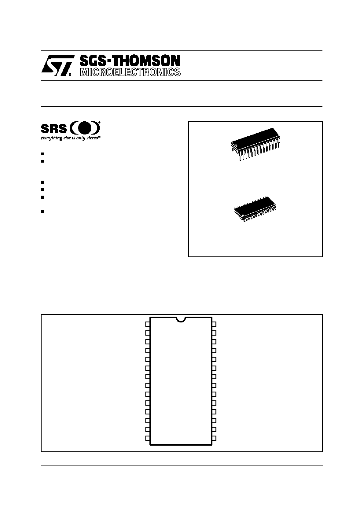
TDA7467
DIP28
ORDERING NUMBER: TDA7467
DESCRIPTION
The TDA7467is a SRS(Sound Retrieval System)
audio matrix. It reproduces SRS sound processing stereo and mono sourcesboth.
The SRS sound is guaranteed by external components and it is not affected by internal process
spreads.
The AC signal setting is obtained by resistor networks and switches combined with operational
amplifiers according to the SRS labs specifica-
PIN CONNECTION(Topview)
LOUT
RIN
LIN
DIG_GND
SCL HP6
ADDR
SDA
AGND
PS1
PS2
PS3
PS4
PS5
PS6
1
2
3
4
5
6
7
8
9
10
11
12
13
14
SO28
ORDERING NUMBER: TDA7467D
tion.
Controlofall thefunctionsisaccomplishedbyserial
bus. Thanks to the used BIPOLAR/CMOS/DMOS
technology, Low Distortion, Low Noise and DC
stepping are obtained.
28
27
26
25
24
22
21
20
19
18
17
16
15
D96AU507
ROUT
CREF
LP2
LP1
HP523
HP4
V
S
HP3
HP2
HP1
VREFOUT
NETW2
NETW1
May 1997
1/11
TDA7467
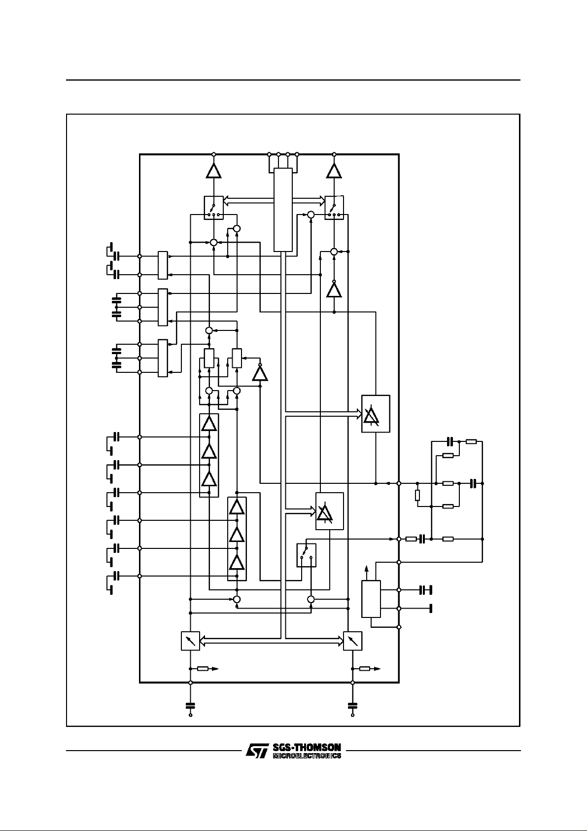
BLOCK DIAGRAM
1
L-OUT
SCL
576
SDA
ADDR
4
DIG_GND
R-OUT
2
D96AU506
C BUS DECODER + LATCHES
2
I
MONO
+
FIX
SRS
MONO
+
SPACE
4.7nF
3.74K
0.47µF
22µF
CREF
AGND
130K
VREFOUT
47.5K
0.47µF
1.5K 32.4K
4.42K
NETW2NETW1
CENTER
1K
15 16
REF
V
SRS
17
-
SUPPLY
MONO
SRS
+
MIX
+
+
+
MIX
-
PHASE SHIFTER 1
PHASE SHIFTER 2
+
FIX
LP1 LP2
LPF1
1µF 0.1µF
HP6
0.1µF
HP5
HPF2
27nF 4.7nF 0.47nF
2.2nF
15nF
100nF
HP4
HP3
HP2
HP1
PS2 PS3
PS1
PS6
PS5
PS4
23
22 24
HPF1
19
18 20
12 13 14 9 10 11 25 26
1µF
0.1µF
1µF
2/11
31.5dB control
0.15µF
S
V
21 8 27
31.5dB
control
50K
3
L-IN
50K
2
R-IN
0.15µF
TDA7467
THERMAL DATA
Symbol Description Value Unit
R
thj-pins
ABSOLUTE MAXIMUM RATINGS
Symbol Parameter Value Unit
V
T
amb
T
QUICK REFERENCEDATA
Symbol Parameter Min. Typ. Max. Unit
V
V
THD Total Harmonic DistortionV = 1Vrms f = 1KHz 0.01 0.1 %
S/N Signal to Noise Ratio V
S
Thermal Resistance Junction-pins Max. 85 °C/W
Operating Supply Voltage 11 V
S
Operating Ambient Temperature -10 to 85 °C
Storage Temperature Range -55 to +150 °C
stg
Supply Voltage 7 9 10.2 V
S
CL
Max. input signal handling 2 Vrms
= 1Vrms (mode = OFF) 106 dB
out
Channel Separation f = 1KHz 90 dB
C
Input Control (0.5dB) -31.5 0 dB
SRS Center Control(1dB step) -31 0 dB
SRS Space Control(1dB step) -31 0 dB
Mute Attenuation 100 dB
ELECTRICALCHARACTERISTICS (referto the test circuit T
V
= 1Vrms;RG= 600Ω, allcontrols flat (G = 0dB), Effect Ctrl = -6dB, MODE = OFF;f = 1KHz
in
=25°C, VS= 9V, RL= 10KΩ,
amb
unless otherwisespecified)
Symbol Parameter Test Condition Min. Typ. Max. Unit
SUPPLY
V
S
I
S
SVR Ripple Rejection L
Supply Voltage 7 9 10.2 V
Supply Current 25 mA
CH/RCH out
, Mode = OFF 60 80 dB
INPUTSTAGE
A
A
A
R
IN
V
CL
VMIN
VMAX
STEP
V
DC
Input Resistance 37.5 50 62.5 K
Clipping Level THD = 0.3% 2 2.5 Vrms
Min. Attenuation -1 0 1 dB
Max. Attenuation 31 31.5 32 dB
Step Resolution -1 0.5 1 dB
DC Steps Adjacent att. step -3 0 3 mV
SRS EFFECT CONTROL
C
range1
Sstep1 Center/SpaceStep Resolution 1 dB
Center/Space Control Range -31 0 dB
Ω
3/11
TDA7467
ELECTRICALCHARACTERISTICS (continued)
Symbol Parameter Test Condition Min. Typ. Max. Unit
AUDIO OUTPUTS
N
N
o(Off)
o(srs)
Output Noise(OFF) Output muted, Flat
BW (20Hz to 20KHz)
Output noise(srs)
BW (20Hz to 20KHz) 50 µVrms
4
5
Surround Sound
d Distortion A
S
C
V
ocl
R
out
V
out
Channel Separation 90 dB
Clipping Level d = 0.3% 2 2.5 Vrms
Output Resistance 30 Ω
DC Voltage Level 3.8 V
=0;Vin= 1Vrms 0.01 0.1 %
V
BUS INPUTS
V
il
V
ih
I
in
V
o
Input Low Voltage 1V
Input High Voltage 3 V
Input Current -5 5 µA
Output VoltageSDA
IO=1.6mA 0.4 V
Acknowledge
SRS SURROUNDSOUND MATRIX
CENTER SRS Control Range -31 0 dB
Step
SPACE SRS Space Control Range -31 0 dB
Step
P
ERSP1
P
ERSP2
L+R L+ R SRS Curve SPACE= MUTE,CENTER=0dB
L, R L, R SRS Curve SPACE= MUTE,CENTER=0dB
Center Step Resolution 1 dB
C
Space Step Resolution 1 dB
S
Perspective 1 Input Signal of 125Hz
12 dB
SPACE= 0dB,CENTER= MUTE
R
= GND; Li
in
Perspective 2 Input Signal of 2.15KHz
n →ROUT
0dB
SPACE= 0dB,CENTER= MUTE
R
= GND; Li
in
n →ROUT
-8.5 dB
R
in = GND; Lin → ROUT
-13.4 dB
R
= GND; Li
in
Lin= GND; Rin→ R
n →LOUT
OUT
Vrms
µ
µVrms
4/11

TDA7467
I2C BUSINTERFACE
Data transmission from microprocessor to the
TDA7467 and viceversa takes place through the
2 wires I
2
C BUS interface, consisting of the two
lines SDA and SCL (pull-up resistors to positive
supply voltage must be connected).
Data Validity
As shown in fig. 3, the data on the SDA line must
be stable during the high period of theclock. The
HIGH and LOW state of the data line can only
change when the clock signal on the SCL line is
LOW.
Start and Stop Conditions
As shown in fig.4 a start condition is a HIGH to
LOW transition of the SDA line while SCL is
HIGH. The stop condition is a LOW to HIGH transition of the SDA line while SCLis HIGH.
Byte Format
Every byte transferred on the SDA line must contain 8 bits. Each byte must be followed by an ac-
2
Figure 3: DataValidityon theI
CBUS
knowledgebit. The MSBis transferredfirst.
Acknowledge
The master (µP)puts a resistiveHIGHlevelon the
SDA line during the acknowledgeclock pulse (see
fig. 5). The peripheral (audioprocessor) that acknowledges has to pull-down (LOW) the SDA line
duringthisclockpulse.
The audioprocessor which has been addressed
has to generate an acknowledge after the reception of each byte, otherwise the SDA line remains
at the HIGH level during the ninth clock pulse
time. In this case the master transmitter can generate the STOP information in order to abort the
transfer.
Transmissionwithout Acknowledge
Avoiding to detect the acknowledge of the audioprocessor,the µP can use a simpler transmission:
simply it waits one clock without checking the
slaveacknowledging,and sends the new data.
This approach of course is less protected from
misworking.
Figure 4: TimingDiagram of I
2
Figure 5: Acknowledgeon the I
CBUS
2
CBUS
5/11

TDA7467
SOFTWARESPECIFICATION
InterfaceProtocol
The interfaceprotocol comprises:
A startcondition (S)
CHIP ADDRESS SUBADDRESS DATA1to DATAn
MSB LSB MSB LSB MSB LSB
S100000A0ACKB DATA ACK DATA ACKP
A chip addressbyte
A subaddressbytes
A sequenceof data (N byte + achnowledge)
A stopcondition (P)
ACK = Achnowledge
S = Start
P = Stop
B = Auto Increment
EXAMPLES
No IncrementalBus
The TDA7467receives a start condition,the correctchip address, a subaddresswith the MSB= 0 (no incrementalbus), N-data (all these data concernthe subaddressselected), a stopcondition.
CHIP ADDRESS SUBADDRESS DATA
MSB LSB MSB LSB MSB LSB
S 1 0 0 0 0 0 A 0 ACK 0 X X X X X D1 D0 ACK DATA ACK P
Incremental Bus
The TDA7467receives a start condition,the correctchip address, a subaddresswith the MSB= 1 (incremental bus): now it is in a loop condition with an autoincrease of the subaddress whereas SUBADDRESS from ”1XXXX1XX”to ”1XXX1111”of DATAare ignored.
The DATA 1 concerns the subaddress sent, and the DATA 2 concerns the subaddress plus one sent in
the loop etc. and at the end, it receivesthe stop condition.
CHIP ADDRESS SUBADDRESS DATA 1to DATAn
MSB LSB MSB LSB MSB LSB
S 1 0 0 0 0 0 A 0 ACK 1 X X X X X D1 D0 ACK DATA ACK P
6/11

TDA7467
DATA BYTES(Address= 80(HEX) ifADDR pin is floating,82(HEX) if ADDRpin is connectedto V
FUNCTIONSELECTION:
The first byte (subaddress)
MSB LSB SUBADDRESS
D7 D6 D5 D4 D3 D2 D1 D0
B X X X X X 0 0 MODE
B X X X X X 0 1 SRS/SPACEATTENUATION
B X X X X X 1 0 SRS/CENTERATTENUATION
B X X X X X 1 1 INPUT ATTENUATION
B = 1: INCREMENTAL BUS; ACTIVE
B = 0: NO INCREMENTAL BUS
X = INDIFFERENT 0, 1
INPUT ATTENUATION SELECTION
MSB LSB INPUT ATTENUATION
D7 D6 D5 D4 D3 D2 D1 D0 0.5 dB STEPS
000 0
0 0 1 -0.5
010 -1
0 1 1 -1.5
100 -2
1 0 1 -2.5
110 -3
1 1 1 -3.5
4 dB STEPS
0000 0
0001 -4
0010 -8
0011 -12
0100 -16
0101 -20
0110 -24
0111 -28
1 MUTE
):
S
INPUT ATTENUATION = 0 ∼ -31.5dB
SRS MODE
D7 D6 D5 D4 D3 D2 D1 D0 MODE
X 0 SRSOFF (FIX)
X 1 SRSON
0 1 MONO SRS (MONO 3D)
1 1 STEREO SRS (STEREO 3D)
RECOMMENDED TO ATTENUATE -3dB ON ”SRS OFF”
ie. MONO SRS (MONO 3D): XXXXXX01
7/11

TDA7467
SPACE & CENTER ATTENUATION SELECTION
MSB LSB SPACE & CENTER ATT.
D7 D6 D5 D4 D3 D2 D1 D0 1 dB STEPS
000 0
001 -1
010 -2
011 -3
100 -4
101 -5
110 -6
111 -7
8 dB STEPS
000 0
001 -8
010 -16
011 -24
1XXXXX MUTE
X = INDIFFERENT 0, 1
SPACE & CENTER ATTENUATION = 0dB
POWERON RESET
-31dB
∼
INPUT MUTE
MODE OFF (FIX)
SPACE ATTENUATION MUTE (MIN)
CENTER ATTENUATION MUTR (MIN)
8/11

DIP28 PACKAGE MECHANICAL DATA
TDA7467
DIM.
MIN. TYP. MAX. MIN. TYP. MAX.
a1 0.63 0.025
b 0.45 0.018
b1 0.23 0.31 0.009 0.012
b2 1.27 0.050
D 37.34 1.470
E 15.2 16.68 0.598 0.657
e 2.54 0.100
e3 33.02 1.300
F 14.1 0.555
I 4.445 0.175
L 3.3 0.130
mm inch
9/11

TDA7467
SO28 PACKAGEMECHANICAL DATA
DIM.
MIN. TYP. MAX. MIN. TYP. MAX.
A 2.65 0.104
a1 0.1 0.3 0.004 0.012
b 0.35 0.49 0.014 0.019
b1 0.23 0.32 0.009 0.013
C 0.5 0.020
c1 45°(typ.)
D 17.7 18.1 0.697 0.713
E 10 10.65 0.394 0.419
e 1.27 0.050
e3 16.51 0.65
F 7.4 7.6 0.291 0.299
L 0.4 1.27 0.016 0.050
mm inch
S8°(max.)
10/11

TDA7467
Information furnished is believed to be accurate and reliable. However, SGS-THOMSON Microelectronics assumes no responsibility for the
consequences of useof such information nor for any infringement of patents or other rights of third parties which may result from its use. No
license is granted by implication or otherwise under any patent or patentrights of SGS-THOMSONMicroelectronics. Specification mentioned
in this publication are subject to change without notice. This publication supersedes and replaces all information previously supplied.
SGS-THOMSON Microelectronics products are not authorized foruseas criticalcomponentsin lifesupport devices or systems withoutexpress
written approval of SGS-THOMSON Microelectronics.
1997 SGS-THOMSON Microelectronics– Printedin Italy– AllRightsReserved
The SoundRetrieval System and are registered trademarks ofSRS Labs,Inc.
SGS-THOMSON Microelectronics GROUP OF COMPANIES
Australia - Brazil- Canada- China- France- Germany- HongKong- Italy- Japan- Korea- Malaysia - Malta- Morocco- TheNetherlands-
Singapore- Spain- Sweden- Switzerland- Taiwan- Thailand- UnitedKingdom- U.S.A.
11/11
 Loading...