

SGS Thomson Microelectronics TDA7460ND Datasheet
CAR RADIO SIGNAL PROCESSOR
DEVICE INCLUDES AUDIO PROCESSOR,
STEREO DECODER, NOISEBLANKER AND
MULTIPATHDETECTOR
HIGH PERFORMANCE SIGNAL PROCESSOR
NO EXTERNALCOMPONENTSREQUIRED
FULLY PROGRAMMABLEVIAI
LOW DISTORTION
LOW NOISE
2
C BUS
TDA7460N
SO20
DESCRIPTION
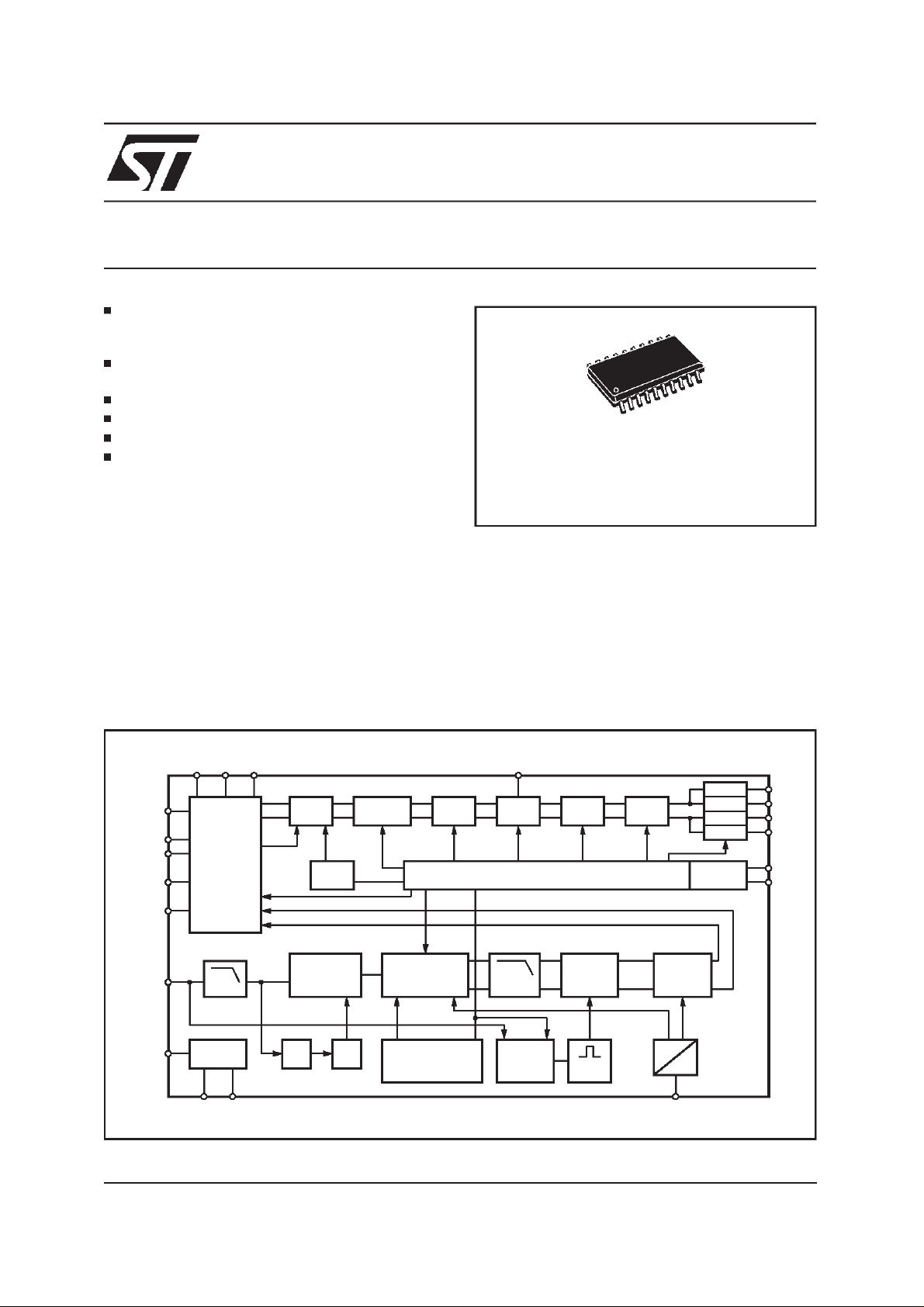
The TDA7460N is a high performance signal
processor specifically designed for car radio applications.
The device includes a complete audioprocessor
and a stereo decoder with noiseblanker,
stereoblend and all signal processing functions
necessary for state-of-the-artas well as future car
radio systems.
Switched-capacitors design technique allows to
obtain all these features without external compo-
BLOCK DIAGRAM
PHONE
(MPOUT)
CASS R
CASS L
PHONE
(MPIN)
GND
AM
CDL CDG CDR
8
1
INPUT
2
MULTIPLEXER
7
AUTO ZERO
6
345 11 17
MIXING
STAGE
PHONE
+
FM R
FM L
LOUDNESS
BEEP
ORDERING NUMBER: TDA7460ND
nents or adjustments. This means that higher
quality and reliability walks alongside an overall
cost saving.
The CSP is fully programmable by I
face allowingto customize key device parameters
and especiallyfilter characteristics.
The BICMOS process combined with the optimized signal processing assure low noise and
low distortionperformances.
SMUTE
OUT LR
VOLUME BASSTREBLE
SOFT
MUTE
DIGITAL CONTROL
OUT LF
OUT RR
OUT RF
2
C BUS
I
2
C bus inter-
OUT LR
19
OUT LF
16
OUT RR
18
OUT RF
12
SCL
13
SDA
MPX
V
June 2000
9
80KHz
LP
15
SUPPLY
S
14 20
CREF
GND
PILOT
CANCELLATION
PLL
PIL
DET
DEMODULATOR
+ STEREO
ADJUST
+ STEREO BLEND
MULTIPATH-
DETECTOR
25KHz
LP
NOISE
BLANKER
S&H
PULSE
FORMER
HIGH
CUT
CONTROL
D
A
10
LEVEL
D97AU629A
1/31

TDA7460N
ABSOLUTE MAXIMUM RATINGS
Symbol Parameter Value Unit
V
S
amb Operating Ambient Temperature Range -40 to 85 °C
T
stg Storage Temperature Range -55 to 150 °C
T
SUPPLY
Symbol Parameter Test Condition Min. Typ. Max. Unit
S Supply Voltage 7.5 9 10 V
V
S Supply Current V
I
SVRR Ripple Rejection @ 1KHz Audioprocessor (all filters flat) 60 dB
ESD
All pins are protected against ESD according to the MIL883standard.
PIN CONNECTION
Operating Supply Voltage 10.5 V
=9V 253035mA
S
Stereodecoder + Audioprocessor 45 dB
CASS R
CASS L
CDR
CDGND
CDL
PHGND (MPOUT)
PHONE (MPIN)
AM
MPX SCL
LEVEL SMUTE
2
3
4
5
6
7
8
9
10
20
19
18
17
16
15
14
13
12
11
D97AU628A
CREF1
OUT LF
OUT RF
OUT LR
OUT RR
V
S
GND
SDA
THERMAL DATA
Symbol Parameter Value Unit
R
th-j pins
Thermal Resistance Junction-pins Max 85 °C/W
2/31

TDA7460N
PIN DESCRIPTION
N. Name Function Type
1 CASSR Cassette Input Right I
2 CASSL Cassette Input Left I
3 CDR CD Right ChannelInput I
4 CDGND Ground reference CD I
5 CDL CD Left ChannelInput I
6 PHGND Phone Ground (MPOUT selectable by SW
7 PHONE Phone Input (MPIN selectable by SW
8 AM AM Input I
9 MPX FM Input (MPX) I
10 LEVEL Level Input Stereodecoder I
11 SMUTE Soft Mute Drive I
12 SCL I
13 SDA I
2
C Clock Line I/O
2
C Data Line I/O
14 GND Supply Ground S
15 VS Supply Voltage S
16 OUTRR Right Rear Speaker Output O
17 OUTLR Left Rear Speaker Output O
18 OUTRF Right Front Spaeaker Output O
19 OUTLF Left Front Speaker Output O
20 CREF Reference Capacitor Pin S
1
)I
1
)I
(1) See input configuration tree and databyte specification ”configuration”
Pin type legenda:
I = Input
O = Output
I/O = Input/Output
S = Supply
3/31

TDA7460N
AUDIO PROCESSORPART
Input Multiplexer
Fully differential or quasi-differential CD and
cassettestereo input
AM monoor stereoinput
Phonedifferential or single ended input
Bass Control
2nd order frequencyresponse
Center frequencyprogrammablein 4(5) steps
DC gain programmable
7 x2dB steps
Internalbeep with 2 frequencies(selectable)
Mixablephone and beep signals
Treble Control
2nd order frequencyresponse
Loudness
Firstor second order frequencyresponse
Center frequencyprogrammablein 4 steps
7 x2dB steps
Program mablecenterfrequencyand qualityfactor
15 x 1dB steps
Selectableflat-mode (constantattenuation)
Speaker Control
4 independentspeaker controls (1dB steps
controlrange 50dB)
Volume control
1dB attenuator
Max. gain 20dB
Max. attenuation79dB
Soft-stepgain control
ELECTRICALCHARACTERISTICS (V
S = 9V; Tamb =25°C; RL = 10KΩ;all gains = 0dB; f = 1KHz;
Mute Functions
Direct mute
Digitally controlled softmute with 4 program-
mabletime constants
unless otherwisespecified).
Symbol Parameter Test Condition Min. Typ. Max. Unit
INPUTSELECTOR
Rin Input Resistance all inputs except Phone 70 100 130 KΩ
Clipping Level 2.2 2.6 V
Input Separation 80 100 dB
Min. Input Gain -1 0 1 dB
Max. Input Gain 13 14 15 dB
Step Resolution 1 2 3 dB
DC Steps Adjacent Gain Step -5 0 +5 mV
to G
G
MIN
MAX
-5 1 +5 mV
G
G
G
V
CL
S
IN
IN MIN
IN MAX
STEP
V
DC
DIFFERENTIAL CD STEREO INPUT
R
in
CMRR Common Mode Rejection Ratio V
N Output Noise @ Speaker
e
Input Resistance Differential 70 100 130 K
Common Mode 20 30 40 K
@ 1KHz 45 70 dB
915µV
Output
CM=1VRMS
CM =1VRMS @ 10KHz 45 60 dB
V
20Hz to 20KHz flat; all stages
0dB
DIFFERENTIAL PHONE INPUT
Rin Input Resistance Differential 10 15 20 KΩ
Common Mode 20 30 40 K
CMRR Common Mode Rejection Ratio V
CM=1VRMS
V
CM=1VRMS
@ 1KHz 45 70 dB
@ 10KHz 45 60 dB
RMS
Ω
Ω
Ω
4/31

TDA7460N
ELECTRICALCHARACTERISTICS
(continued)
Symbol Parameter Test Condition Min. Typ. Max. Unit
BEEPCONTROL
VRMS Beep Level 250 350 500 mV
BMIN Lower Beep Frequency 570 600 630 Hz
f
f
BMAX
Higher Beep Frequency 1.15 1.2 1.25 KHz
MIXINGCONTROL
MLEVEL Mixing Level Source -1 0 1 dB
Source -5 -6 -7 dB
Source -10 -12 -14 dB
Beep/Phone -1 0 1 dB
VOLUMECONTROL
G
MAX
A
MAX
A
STEP
E
A
T Tracking Error 2dB
E
DC DC Steps Adjacent Attenuation Steps -3 0.1 3 mV
V
Max Gain 19 20 21 dB
Max Attenuation -83 -79 -75 dB
Step Resolution 0.5 1 1.5 dB
Attenuation Set Error G = -20 to 20dB -1.25 0 1.25 dB
G = -60 to 20dB -4 0 3 dB
From 0dB to G
MIN -7 0.5 +7 mV
LOUDNESSCONTROL
A
STEP
A
MAX
CMIN Lower Center Frequency 180 200 220 Hz
f
CMAX Higher CenterFrequency 360 400 440 Hz
f
Step Resolution 0.5 1 1.5 dB
Max. Attenuation -16 -15 -14 dB
SOFTMUTE
A
MUTE
T
D
THlow Low Threshold for SM Pin
V
THhigh High Threshold for SM Pin 2.5 V
V
PU Internal Pull-up Resistor 70 100 130 KΩ
R
V
PU
Mute Attenuation 60 100 dB
Delay Time T1 0.48 1 ms
T2 0.96 2 ms
T3 20 40.4 60 ms
T4 200 324 600 ms
1
Pull-up Voltage 4.7 V
SOFTSTEP
T
SW
1) The SM pin is active low (Mute = 0)
Switch Time 5 10 15 ms
1V
5/31
TDA7460N
ELECTRICALCHARACTERISTICS
(continued)
Symbol Parameter Test Condition Min. Typ. Max. Unit
BASSCONTROL
CRANGE Control Range ±13 ±14 ±15 dB
A
STEP Step Resolution 1 2 3 dB
f
C
Q
BASS Quality Factor Q1 0.9 1 1.1
DC
GAIN
Center Frequency f
C1
f
C2
f
C3
f
C4
Q
2 1.1 1.25 1.4
Q
3
Q
4
54 60 66 Hz
63 70 77 Hz
72 80 88 Hz
90 100
(2)
110 Hz
1.3 1.5 1.7
1.8 2 2.2
Bass-Dc-Gain DC = off -1 0 +1 dB
DC = on 4 4.4 6 dB
TREBLECONTROL
C
A
RANGE
STEP
f
C
Control Range
13
±
14
±
15 dB
±
Step Resolution 1 2 3 dB
Center Frequency f
C1
f
C2 10 12.5 15 KHz
f
C3
f
C4
8 10 12 KHz
12 15 18 KHz
14 17.5 21 KHz
SPEAKERATTENUATORS
CRANGE Control Range -53 -50 -47 dB
A
A
STEP
MUTE
E
V
DC
E
Step Resolution 0.5 1 2 dB
Output Mute Attenuation 80 90 dB
Attenuation Set Error -2 2 dB
DC Steps Adjacent Attenuation Steps 0.1 5 mV
AUDIO OUTPUTS
V
CLIP
R
L
C
L Output LoadCapacitance 10 nF
R
OUT Output Impedance 30 100 Ω
V
DC
Clipping Level d = 0.3% 2.2 2.6 V
Output Load Resistance 2 K
DC Voltage Level 3.6 3.8 4.0 V
GENERAL
e
NO
S/N Signal to Noise Ratio all gain= 0dB flat; V
d Distortion V
S
C Channel separation Left/Right 80 100 dB
E
T
2) See description of Audioprocessor Part - Bass & Treble filter characteristics programming
Output Noise BW = 20 Hz to 20 KHz
315µV
output muted
BW = 20 Hz to 20 KHz
6.5 15 µV
all gain = 0dB
=2V
O
RMS
bass treble at12dB; V
2.6V
RMS
=1V
IN
V
IN =1VRMS;Bass& Treble= 12dB 0.05 0.1 %
; all stages0dB 0.002 0.1 %
RMS
O =
106 dB
100 dB
Total Tracking Error AV= 0 to -20dB -1 0 1 dB
A
= -20 to -60dB -2 0 2 dB
V
RMS
Ω
6/31

TDA7460N
DESCRIPTIONOFTHE AUDIOPROCESSOR
PART
ProgrammableInput Matrix
The programmableinput matrix of the TDA7460N
offers several possibilities to adapt the audioprocessor to the desired application. In to the standard applicationwe have:
CD quasi differential
Cassettestereo
Phonedifferential
AM mono
Stereodecoderinput.
The input matrixcan be configuredby only 2 bits:
Figure 1. InputConfiguration Tree
bits 3 and 4 of subaddress 0. Basically the bit of
subaddress 13 is fixed by the applicationand has
to be programmed only once at the startup of the
IC.
For many configurations the two bits are also
fixed during one application(e.g.the standardapplication) and a change of the input source can
be done by loading the first three bits of subaddress 0.
In other configurations for some sources a programming of bit 3 and 4 of subaddress0 is necessary in addition to the three source selection
bits. In every case only the subaddress 0 has to
be changedto switch from one sourceto another.
The followingpicture shows the input and source
programmingflow:
TDA7460
NO
MULTIPATH
CD QD CD FD
APPL. 2APPL. 1 APPL. 3 APPL. 5APPL. 4 APPL. 6
CD QD
CASSETTE
FM STD
AM MONO
PHONE (D)
Note: in AMSTD configuration theAM monosignal is lead through the FMstereodecoderpart touse its additionalfilters and high-cutfunction.
CD QD
CASSETTE
FM STD
AM
STEREO
PHONE (SE)
CD QD
CASSETTE
FM STD
AM STD
PHONE (D)
CD FD
CASSETTE
FM STD
AM MONO
PHONE (SE)
CD FD
CASSETTE
FM STD
AM STEREO
CD FD
CASSETTE
FM STD
AM STD
PHONE (SE)
CD QD
CASSETTE
FM STD
AM MONO
CD QD
MULTIPATH
APPL. 8APPL. 7
CD QD
CASSETTE
FM STD
AM STD
CD FD
D98AU851
7/31

TDA7460N
PIN NUMBER
Appl. No 4 6 7 8 Programming
1CD
2CD
3CD
4 CDR
5 CDR
6 CDR
7CD
8CD
1)
Syntax 0/xxx11100 means: SUBADDRESS= 0 - DATA BYTE = xxx11100 (x - don’t care)
GND
GND
GND
GND CDLGND Phone AMMONO Startup: 0/xxxx0xxx
GND CDLGND AMRIGHT AMLEFT Startup: 0/xxxx0xxx
GND
GND MPOUT MPIN AMMONO Startup: 0/xxx11xxx
GND MPOUT MPIN AMSTD Startup: 0/xxx1xxx
How to find the right input configuration
The best way to come to the desired configuration may be to go through the application tree
from the top to the bottom while making the specific decisions.
This way will lead to one of the six possibleapplications. Then take the number of the application
and go into the pinning table. Here you will find
the special pinout as well as the specialprogramming codes for selecting sources.
For example in Appl. 6 the TDA7460N has to be
configured while startup with the databyte
0/xxxx0xxx.
To select the FM, AM or phone source the last
five significant bits of subaddress 0 have to be
changed, for any other source the last three bits
are sufficient(see data byte specification).
Input stages
Most of the input circuits are the same as in preceeding ST audioprocessors with exception of
the CD inputs (see figure2).
In the meantime there are some CD players in
the market having a significant high source impedance which affects strongly the commonmode rejection of the normal differential input
stage. The additional buffer of the CD input
Phone
GND
Phone AM
Phone
GND
CDL
GND
Phone AM
Phone AMSTD Startup: 0/xxxx1xxx
Phone AMSTD Startup: 0/xxxx0xxx
RIGHT
Startup: 0/xxx11xxx
Startup: 0/xxxx1xxx
FM
AM
Phone
FM
AM
Phone
FM
AM
FM
AM
Phone
FM
AM
AM
MONO
LEFT
avoids this drawbackand offers the full commonmoderejection even with those CD players.
The TDA7460N can be configured with an additional input; if the AC couplingbefore the speaker
stage is not used (bit 7 in subaddress5set to ”1”)
ACINL and ACINR pins can be used as an additional stereo input.
AutoZero
In order to reduce the number of pins there is no
AC coupling between the In-Gain and the following stage, so that any offset generated by or before the In-Gain stage would be transferred or
even amplified to the output.
To avoid that effect a special offset cancellation
stage called AutoZerois implemented.
To avoid audible clicks the audioprocessor is
muted before the loudness stage during this time.
In some cases, for example if the µP is executing
a refresh cycle of the I
2
C bus programming, it is
not usefulto start a newAutoZero action because
no newsource is selectedand an undesiredmute
would appear at the outputs. For such applications the TDA7460N could be switched in the
”Auto Zero Remain” mode (Bit 6 of the subaddress byte). If this bit is set to high, the DATABYTE 0 could be loaded without invoking the
AutoZeroand the old adjustmentvalue remains.
1)
0/xxx11100
0/xxx01011
0/xxx11010
0/xxx11100
0/xxx01100
0/xxx11010
0/xxx10100
0/xxx00011
0/xxx10100
0/xxx00100
0/xxx10010
0/xxx11100
0/xxx01100
8/31
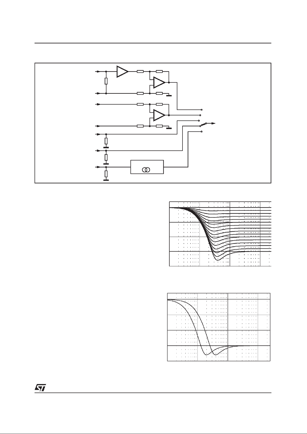
Figure 2. Inputstages
TDA7460N
CD
100K
CDGND
PHONE
PH_GND
CASSETTE
100K
AM
100K
MPX
100K
15K 15K
15K 15K
15K 15K
15K 15K
STEREODECODER
Mixing Stage
This stage offers the possibilityto mix the internal
beep or the phone signal to any other source.
Due to the fact that the mixing stage is also located behind the In-Gain stage fine adjustments
of the main source level can be donein this way.
-
+
-
+
IN GAIN
D97AU633A
Figure 3. Loudness Attenuation @ fc = 400Hz
(secondorder)
0.0
-5.0
Loudness
There are four parameters programmable in the
loudnessstage (see fig. 3, 4, 5):
- Attenuation
- Center Frequency
- LoudnessQ
- Flat Mode: in this mode the loudnessstageworks
asa 0 - 15dBattenuator.
Softmute
The digitally controlled softmute stage allows
muting/demuting the signal with a I
grammable slope. The mute process can either
be activated by the softmute pin or by the I
2
C bus pro-
2
bus. The slope is realized in a special S shaped
curve to mute slow in the critical regions (see figure 6).
For timing purposes the Bit 3 of the I
2
C bus output registeris set to 1 from the start of muting until the end of demuting.
-10.0
-15.0
-20.0
10.0 100.0 1.0K 10.0K
Figure 4. Loudness Center frequency @ Attn.
= 15dB (second order)
0.0
-5.0
-10.0
C
-15.0
-20.0
10.0 100.0 1.0K 10.0K
9/31

TDA7460N
Figure 5. Loudness @ Attn.= 15dB, fc = 400Hz
(dB)
-5
-10
-15
-20
10 100 1,000 Hz
D98AU844
Softstep Volume
When volume level is changed often an audible
click appears at the output. The root cause of
those clicks could be either a DC offset before
the volume stage or the sudden change of the
envelope of the audio signal. With the Softstep
feature both kinds of clickscould be reduced to a
minimum and are no moreaudible(see figure 7).
Bass
There are three parameters programmable in the
bass stage (see figs 8, 9, 10,11):
Figure 6. Softmute Timing
1
EXT.
MUTE
+SIGNAL
REF
-SIGNAL
1
2
I
C
BUS
OUT
D97AU634
Note: Please notice that a startedMute actionis always terminated
and could not be interrupted by a change of the mute signal.
Time
Figure 7. SoftStep Timing
VOUT
2dB
1dB
- Attenuation
- Center Frequency (60, 70, 80 and 100Hz)
- Quality Factors (1, 1.25, 1.5 and 2)
DC Mode
In this mode the DC gain is increased by 4.4dB.
In addition the programmed center frequencyand
quality factor is decreased by 25% which can be
used to reach alternative center frequencies or
quality factors.
Treble
There are two parameters programmable in the
treblestage (see figs 12, 13):
- Attenuation
- Center Frequency (10, 12.5, 15 and17.5kHz).
Speaker Attenuator
Due to practicalaspects the stepsin the speaker
attenuators are not linear over the full range. At
attenuations more than 24dB the steps increase
from 1.5dB to 10dB (please see data byte specification).
10ms
-1dB
-2dB
Note: For steps more than 1dB the softstep mode should be
deactivated because it could generate a 1dB error during the
blend-time
Time
D97AU635
10/31
 Loading...