

DIGITALLY CONTROLLED AUDIO PROCESSOR
INPUTMULTIPLEXER
- 2 STEREO INPUTS
- SELECTABLEINPUT GAIN FOR OPTIMAL
ADAPTATIONTO DIFFERENT SOURCES
ONE STEREO OUTPUT
TREBLE, AND BASS CONTROL IN 2.0dB
STEPS
VOLUMECONTROL IN 1.0dB STEPS
TWOSPEAKERATTENUATORS:
- TWOINDEPENDENTSPEAKERCONTROL
IN 1.0dBSTEPS FOR BALANCEFACILITY
- INDEPENDENT MUTE FUNCTION
ALL FUNCTION ARE PROGRAMMABLE VIA
SERIALBUS
TONE CONTROL
DIP20
ORDERING NUMBER:
TDA7449
TDA7449
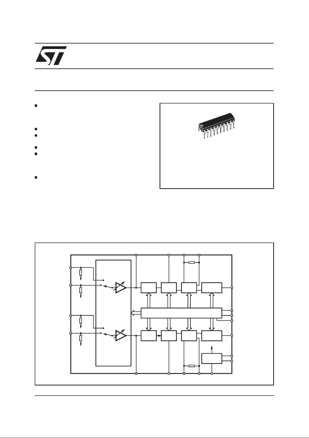
DESCRIPTION
The TDA7449 is a volume tone (bass and treble)
balance (Left/Right) processor for quality audio
applicationsin TV systems.
Selectable input gain is provided. Control of all
the functions is accomplishedby serialbus.
BLOCK DIAGRAM
MUXOUTL
10 16 15 14
8
L-IN1
L-IN2
R-IN1
R-IN2
100K
9
100K
7
100K
6
100K
G
0/30dB
2dB STEP
G
VOLUME
VOLUME
The AC signal setting is obtained by resistor networks and switches combined with operational
amplifiers.
Thanks to the used BIPOLAR/CMOSTechnology,
Low Distortion, Low Noise and DC stepping are
obtained.
TREBLE(L)
TREBLE
I2CBUS DECODER + LATCHES
TREBLE
BIN(L)
BASS
BASS
BOUT(L)
R
B
SPKR
LEFT
SPKR
RIGHT
5
ATT
ATT
V
REF
19
20
18
4
LOUT
SCL
SDA
DIG_GND
ROUT
April 1999
INPUT
MULTIPLEXER
+ GAIN
R
B
11 17 12 13 1
MUXOUTR TREBLE(R)
BIN(R) BOUT(R)
SUPPLY
CREF
2
V
3
AGND
D98AU847A
S
1/17
TDA7449
ABSOLUTE MAXIMUM RATINGS
Symbol Parameter Value Unit
V
S
T
amb
T
stg
PIN CONNECTION
Operating Supply Voltage 10.5 V
Operating Ambient Temperature -10 to 85 °C
Storage Temperature Range -55 to 150 °C
CREF
V
PGND
ROUT
LOUT
R_IN2
R_IN1
L_IN1
L_IN2
1
2
S
3
4
5
6
7
8
9 BIN(R)
19
18
17
16
15
14
13
12
SDA20
SCL
DIG_GND
TREBLE(R)
TREBLE(L)
BIN(L)
BOUT(L)
BOUT(R)
MUXOUT(L) 10 MUXOUT(R)11
D98AU848
THERMAL DATA
Symbol Parameter Value Unit
R
thj-pin
Thermal ResistanceJunction-pins 150 °C/W
QUICK REFERENCE DATA
Symbol Parameter Min. Typ. Max. Unit
V
S
V
CL
THD Total Harmonic DistortionV = 1Vrms f = 1KHz 0.01 0.1 %
S/N Signal to Noise Ratio V
S
C
2/17
Supply Voltage 6 9 10.2 V
Max. input signal handling 2 Vrms
= 1Vrms (mode = OFF) 106 dB
out
Channel Separation f = 1KHz 90 dB
Input Gain in (2dBstep) 0 30 dB
Volume Control (1dB step) -47 0 dB
Treble Control (2dB step) -14 +14 dB
Bass Control (2dB step) -14 +14 dB
Balance Control 1dB step -79 0 dB
Mute Attenuation 100 dB
TDA7449
ELECTRICALCHARACTERISTICS
R
= 600Ω, all controls flat (G = 0dB), unless otherwise specified)
G
(refer to the test circuit T
=25°C,VS= 9V,RL= 10KΩ,
amb
Symbol Parameter Test Condition Min. Typ. Max. Unit
SUPPLY
V
S
I
S
SVR Ripple Rejection 60 90 dB
Supply Voltage 6 9 10.2 V
Supply Current 7 mA
INPUT STAGE
G
G
R
V
S
inmin
inman
G
IN
CL
IN
step
Input Resistance 100 KΩ
Clipping Level THD = 0.3% 2 2.5 Vrms
Input Separation The selected input is grounded
80 100 dB
through a 2.2µ capacitor
Minimum Input Gain -1 0 1 dB
Maximum Input Gain 30 dB
Step Resolution 2 dB
VOLUMECONTROL
C
RANGE
A
A
V
A
VMAX
STEP
E
A
E
T
DC
mute
Control Range 45 47 49 dB
Max. Attenuation 45 47 49 dB
Step Resolution 0.5 1 1.5 dB
Attenuation Set Error AV= 0 to-24dB -1.0 0 1.0 dB
A
= -24 to -47dB -1.5 0 1.5 dB
V
Tracking Error AV= 0 to-24dB 0 1 dB
= -24 to -47dB 0 2 dB
A
V
DC Step adjacent attenuation steps
from 0dB to A
V
max
0
0.5
3mV
Mute Attenuation 80 100 dB
BASS CONTROL(1)
Gb Control Range Max. Boost/cut +12.0 +14.0 +16.0 dB
B
STEP
R
B
Step Resolution 1 2 3 dB
Internal Feedback Resistance 18.75 25 31.25 KΩ
TREBLECONTROL(1)
Gt Control Range Max. Boost/cut +13.0 +14.0 +15.0 dB
T
STEP
Step Resolution 1 2 3 dB
SPEAKERATTENUATORS
C
RANGE
S
STEP
E
A
V
DC
A
mute
NOTE1:
1) The device is functionally goodat Vs = 5V. a step down,on Vs, to 4V does’t reset thedevice.
2) BASS and TREBLE response: The centerfrequency and the response quality can be chosen by the external circuitry.
Control Range 76 dB
Step Resolution 0.5 1 1.5 dB
Attenuation Set Error AV= 0 to-20dB -1.5 0 1.5 dB
A
= -20 to -56dB -2 0 2 dB
V
DC Step adjacent attenuation steps 0 3 mV
Mute Attenuation 80 100 dB
mV
3/17
TDA7449
ELECTRICALCHARACTERISTICS
(continued.)
Symbol Parameter Test Condition Min. Typ. Max. Unit
AUDIOOUTPUTS
VCLIP ClippingLevel d = 0.3% 2.1 2.6 VRMS
R
L
R
O
DC DC Voltage Level 3.8 V
V
Output Load Resistance 2 KΩ
Output Impedance 10 40 70
GENERAL
E
NO
E
t
S/N Signal to Noise Ratio All gains 0dB; V
S
C
d Distortion A
Output Noise All gains = 0dB;
515µV
BW = 20Hz to 20KHz flat
Total Tracking Error AV= 0to -24dB 0 1 dB
A
= -24to -47dB 0 2 dB
V
O
=1V
; 106 dB
RMS
Channel Separation Left/Right 80 100 dB
=0;VI=1V
V
; 0.01 0.08 %
RMS
BUS INPUT
V
IL
V
IH
I
IN
V
O
Input Low Voltage 1V
Input High Voltage 3 V
Input Current VIN= 0.4V -5 5 µA
Output Voltage SDA
IO= 1.6mA 0.4 0.8 V
Acknowledge
Ω
4/17
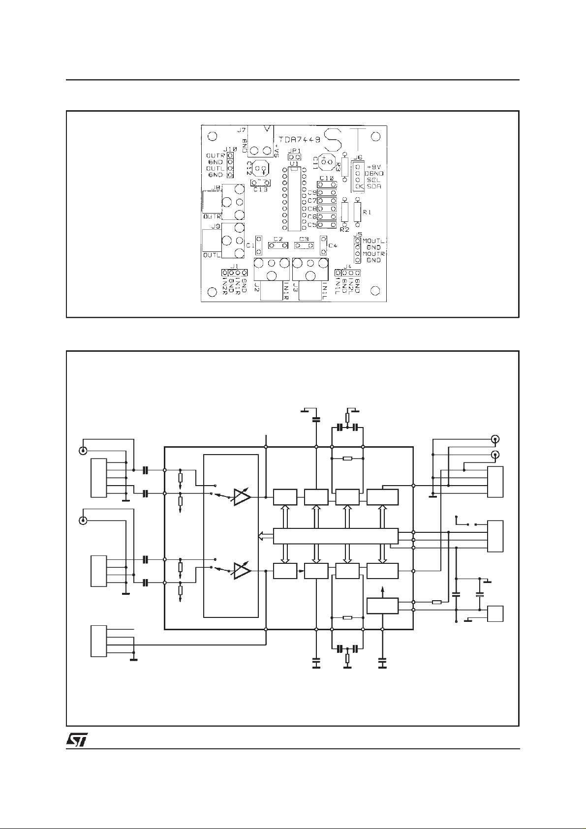
P.C.Board
TEST CIRCUIT
TDA7449
R2 2K
C9
5.6nF
J5
IN1L
J3
RCA
J2
RCA
GND
1
IN1L
2
GND
3
J4
IN2L
4
GND
5
CON3
IN1R
IN2R
1
GND
2
J1
IN1R
3
GND
4
CON
MOUTL
1
GND
2
J5
MOUTR
3
GND
4
CON4
C3 0.47µF
C4 0.47µF
C1 0.47µF
C2 0.47µF
L-IN1
L-IN2
R-IN2
R-IN1
8
100K
9
100K
6
100K
7
100K
INPUT
MUXOUTL
G
0/30dB
2dB STEP
G
MULTIPLEXER
+ GAIN
MUXOUTR TREBLE(R)
TREBLE(L)
10 16 15 14
VOLUME
VOLUME
11 17 12 13 1
5.6nF
150nF 330nF
C8C7
BIN(L)
R
B
TREBLE
I2CBUS DECODER+ LATCHES
TREBLE
C10
BASS
BASS
R
B
BOUT(R)
C5 C6
BIN(R)
150nF 330nF
R1
2K
BOUT(L)
SPKR
SPKR
RIGHT
SUPPLY
LEFT
V
OUT_L
+V8
GND
C12
22µF
1
2
3
4
CON4
1
2
3
4
CON4
1
2
CON2
J8
J9
J10
J6
J7
OUT_R
+9 V
+9V
OUT_L
OUT_ R
JP1
JUMPER
C13
100nF
5
C11
10µF
LOUT
DIG_GND
18
SCL
19
SDA
20
4
ROUT
R3 30
3
AGND
2
V
S
D98AU849A
ATT
ATT
REF
CREF
5/17
TDA7449
APPLICATIONSUGGESTIONS
The first and the last stages are volume control
blocks. The control range is 0 to -47dB (mute) for
the first one, 0 to -79dB (mute) for the last one.
Both of them have 1dB step resolution.
The very high resolution allows the implementation
of systems freefromanynoisyacousticaleffect.
The TDA7449 audioprocessor provides 2 bands
tones control.
Bass, Stages
The Bass cell has an internal resistor Ri = 25K
Ω
typical.
Several filter types can be implemented, connect-
ing external components to the BassIN and OUT
pins.
The fig.1 refers to basic T Type Bandpass Filter
starting from the filter component values (R1 in-
Figure 1.
Ri internal
OUTIN
C
1
C
2
ternal and R2,C1,C2 external) the centre frequency Fc, the gain Av at max. boost and the filter Q factorare computedas follows:
=
F
C
2
⋅ π⋅√
C2 + R2 C1+ Ri C1
R2
=
A
V
R2 C1 + R2 C2
√
Q =
R2 C1
1
Ri, R2, C1, C2
+
Ri R2
C1 C2
+ R2 C2
Viceversa, once Fc, Av, and Ri internal value are
fixed, the external componentsvalues will be:
2
Q
=
⋅ C1
− 1)Q
2
(A
V
2
C1
A
− 1
V
=
π ⋅ R
2 ⋅
R2 =
⋅ Q
i
− 1 − Q
A
V
2 ⋅ π ⋅ C1 ⋅ FC⋅ (AV− 1) ⋅Q
C2
TrebleStage
The treble stage is a high pass filter whose time
constant is fixed by an internal resistor (25KΩ
typical) and an external capacitor connected between treble pins andground
Typical responsesare reported in Figg. 10 to 13.
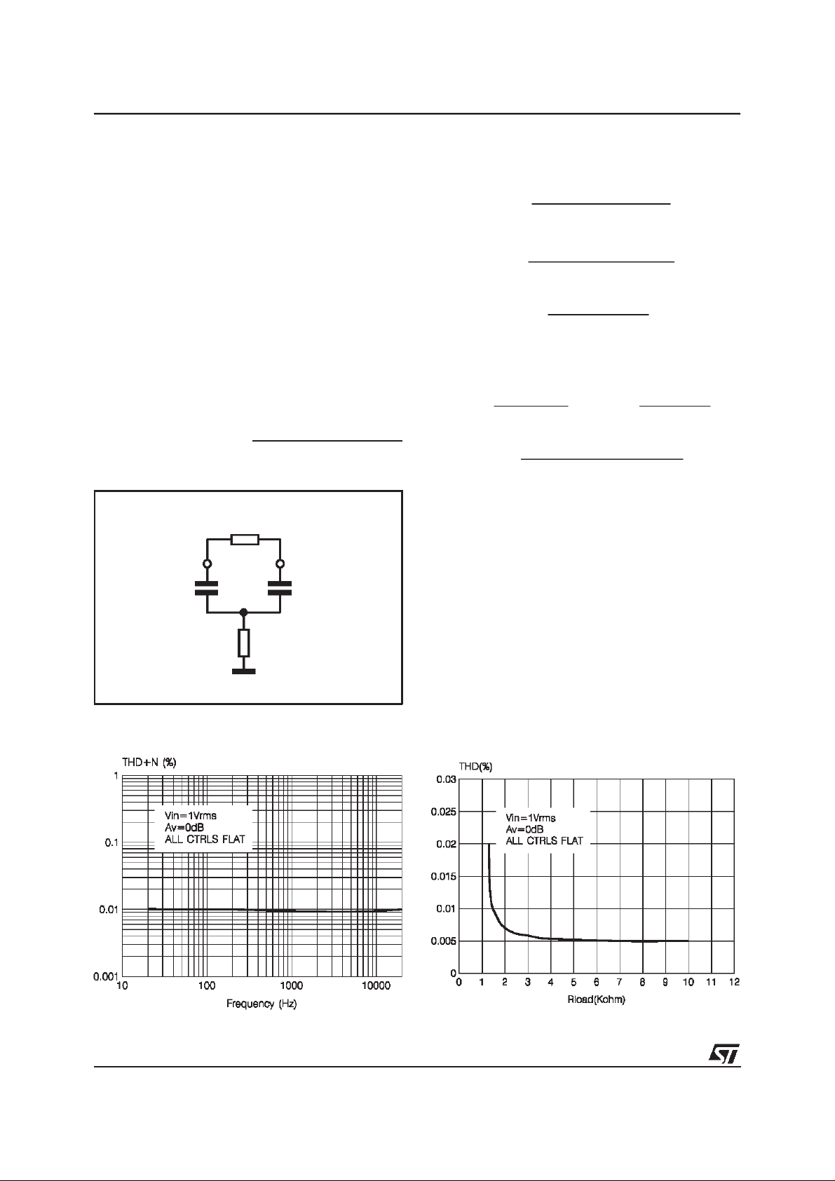
Figure 2:
R
THD vs. frequency
2
D95AU313
CREF
The suggested 10µF reference capacitor (CREF)
value can be reduced to 4.7µF if the application
requiresfasterpower ON.
Figure3:
THDvs. R
LOAD
6/17

TDA7449
Figure 4:
Channelseparationvs. frequency
Figure 6: Trebleresponse
Figure5:
Bassresponse
Ri= 25kΩ
C1 = 150nF
C2 = 330nF
R2= 2kΩ
7/17

TDA7449
2
C BUS INTERFACE
I
Data transmission from microprocessor to the
TDA7449 and vice versa takes place through the
2 wires I
2
C BUS interface, consisting of the two
lines SDA and SCL (pull-up resistors to positive
supply voltage must be connected).
Data Validity
As shown in fig. 3, thedata on the SDA line must
be stable during the high period of the clock. The
HIGH and LOW state of the data line can only
change when the clock signal on the SCL line is
LOW.
Start and Stop Conditions
As shown in fig.4 a start condition is a HIGH to
LOW transition of the SDA line while SCL is
HIGH. The stop condition is a LOW to HIGH transition of the SDA line while SCL is HIGH.
Byte Format
Every byte transferred on the SDA line must contain 8 bits. Each byte must be followed by an ac-
Figure 3:
Data Validityon theI
2
CBUS
knowledgebit. The MSB is transferredfirst.
Acknowledge
The master (µP)puts a resistiveHIGHlevel on the
SDA line during the acknowledge clock pulse (see
fig. 5). The peripheral (audio processor) that acknowledges has to pull-down (LOW) the SDA line
duringthisclock pulse.
The audio processor which has been addressed
has to generate an acknowledge after the reception of each byte, otherwise the SDAline remains
at the HIGH level during the ninth clock pulse
time. In this case the master transmitter can generate the STOP information in order to abort the
transfer.
Transmissionwithout Acknowledge
Avoiding to detect the acknowledge of the audio
processor,the µP canuse a simplertransmission:
simply it waits one clock without checking the
slaveacknowledging,and sends the new data.
This approach of course is less protected from
misworking.
Figure 4:
TimingDiagram of I
2
Figure 5: Acknowledgeon the I
8/17
CBUS
2
CBUS
TDA7449
SOFTWARESPECIFICATION
InterfaceProtocol
The interface protocol comprises:
A start condition (S)
address
A subaddressbytes
A sequenceof data (N byte + acknowledge)
A stopcondition (P)
A chip address byte, containing the TDA7449
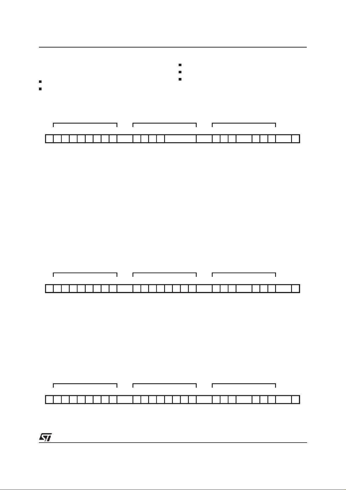
CHIP ADDRESS
MSB LSB MSB LSB MSB LSB
S10001000ACK ACK DATA ACK P
D96AU420
SUBADDRESS DATA 1 to DATA n
X DATA
XXB
ACK = Acknowledge
S = Start
P = Stop
A = Address
B = Auto Increment
EXAMPLES
No IncrementalBus
rect chip address, a subaddress with the B = 0
(no incremental bus), N-data (all these data concern the subaddressselected),a stop condition.
The TDA7449 receives a start condition, the cor-
CHIP ADDRESS
MSB LSB MSB LSB MSB LSB
S10001000ACK ACK DATA ACK P
D96AU421
IncrementalBus
The TDA7449 receive a start conditions, the correct chip address, a subaddress with the B = 1
(incremental bus): now it is in a loop condition
with an autoincrease of the subaddress whereas
CHIP ADDRESS
MSB LSB MSB LSB MSB LSB
S10001000ACK ACK DATA ACK P
D96AU422
SUBADDRESS DATA
XD3
XX0 D2D1D0
SUBADDRESS from ”XXX1000” to ”XXX1111”of
DATAare ignored.
The DATA 1 concern the subaddress sent, and
the DATA 2 concern the subaddress sent plus
one in the loop etc, and at the end it receivers the
stop condition.
SUBADDRESS DATA 1 to DATA n
XD3
XX1 D2D1D0
9/17

TDA7449
POWERON RESET CONDITION
INPUT SELECTION IN2
INPUT GAIN 28dB
VOLUME MUTE
BASS 2dB
TREBLE 2dB
SPEAKER MUTE
DATA BYTES
Address = 88 HEX (ADDR:OPEN).
FUNCTIONSELECTION:First byte (subaddress)
MSB LSB
D7 D6 D5 D4 D3 D2 D1 D0
XXXB00 00INPUT SELECT
XXXB00 01INPUT GAIN
XXXB00 10VOLUME
XXXB00 11NOTALLOWED
XXXB01 00BASS
XXXB01 01TREBLE
XXXB01 10SPEAKER ATTENUATE ”R”
XXXB01 11SPEAKER ATTENUATE ”L”
B = 1: INCREMENTAL BUSACTIVE
B = 0: NO INCREMENTALBUS
X = DON’T CARE
SUBADDRESS
INPUT SELECTION
MSB LSB
D7 D6 D5 D4 D3 D2 D1 D0
XXXXXX00 NOTALLOWED
XXXXXX01 NOTALLOWED
XXXXXX10 IN2
XXXXXX11 IN1
INPUT MULTIPLEXER
10/17

DATA BYTES (continued)
INPUT GAIN SELECTION
MSB LSB INPUT GAIN
D7 D6 D5 D4 D3 D2 D1 D0 2dB STEPS
0000 0dB
0001 2dB
0010 4dB
0011 6dB
0100 8dB
0 1 0 1 10dB
0 1 1 0 12dB
0 1 1 1 14dB
1 0 0 0 16dB
1 0 0 1 18dB
1 0 1 0 20dB
1 0 1 1 22dB
1 1 0 0 24dB
1 1 0 1 26dB
1 1 1 0 28dB
1 1 1 1 30dB
TDA7449
GAIN = 0 to 30dB
VOLUMESELECTION
MSB LSB VOLUME
D7 D6 D5 D4 D3 D2 D1 D0 1dB STEPS
0 0 0 0dB
0 0 1 -1dB
0 1 0 -2dB
0 1 1 -3dB
1 0 0 -4dB
1 0 1 -5dB
1 1 0 -6dB
1 1 1 -7dB
0000 0dB
0 0 0 1 -8dB
0 0 1 0 -16dB
0 0 1 1 -24dB
0 1 0 0 -32dB
0 1 0 1 -40dB
X 1 1 1 X X X MUTE
VOLUME = 0 to 47dB/MUTE
11/17

TDA7449
DATA BYTES (continued)
BASS SELECTION
MSB LSB BASS
D7 D6 D5 D4 D3 D2 D1 D0 2dB STEPS
0 0 0 0 -14dB
0 0 0 1 -12dB
0 0 1 0 -10dB
0 0 1 1 -8dB
0 1 0 0 -6dB
0 1 0 1 -4dB
0 1 1 0 -2dB
0111 0dB
1111 0dB
1110 2dB
1101 4dB
1100 6dB
1011 8dB
1 0 1 0 10dB
1 0 0 1 12dB
1 0 0 0 14dB
TREBLESELECTION
MSB LSB TREBLE
D7 D6 D5 D4 D3 D2 D1 D0 2dB STEPS
0 0 0 0 -14dB
0 0 0 1 -12dB
0 0 1 0 -10dB
0 0 1 1 -8dB
0 1 0 0 -6dB
0 1 0 1 -4dB
0 1 1 0 -2dB
0111 0dB
1111 0dB
1110 2dB
1101 4dB
1100 6dB
1011 8dB
1 0 1 0 10dB
1 0 0 1 12dB
1 0 0 0 14dB
12/17

DATA BYTES (continued)
SPEAKERATTENUATE SELECTION
MSB LSB SPEAKER ATTENUATION
D7 D6 D5 D4 D3 D2 D1 D0 1dB
0 0 0 0dB
0 0 1 -1dB
0 1 0 -2dB
0 1 1 -3dB
1 0 0 -4dB
1 0 1 -5dB
1 1 0 -6dB
1 1 1 -7dB
0000 0dB
0 0 0 1 -8dB
0 0 1 0 -16dB
0 0 1 1 -24dB
0 1 0 0 -32dB
0 1 0 1 -40dB
0 1 1 0 -48dB
0 1 1 1 -56dB
1 0 0 0 -64dB
1 0 0 1 -72dB
1 1 1 1 X X X MUTE
TDA7449
SPEAKER ATTENUATION = 0 to-79dB/MUTE
PIN: 1
V
S
V
S
20K
CREF
20K
D96AU430
PINS: 4,5
ROUT
LOUT
D96AU434
V
S
24
20µA
13/17

TDA7449
PINS: 6,7,8,9
V
S
IN
PINS: 12, 15
PINS: 10,11
V
S
20µA
MUXOUT
100K
V
REF
D96AU425
V
S
20µA
GND
D96AU491
PINS: 13, 14
V
S
20µA
V
S
20µA
BIN(L)
BIN(R)
PINS:
14/17
16, 17
TREBLE(L)
TREBLE(R)
25K
44K
BOUT(L)
PIN:
BOUT(R)
19
D98AU850
V
S
20µA
D96AU429
20µA
SCL
50K
D96AU433
D96AU424

PIN: 20
SDA
TDA7449
20µA
D96AU423
15/17
TDA7449
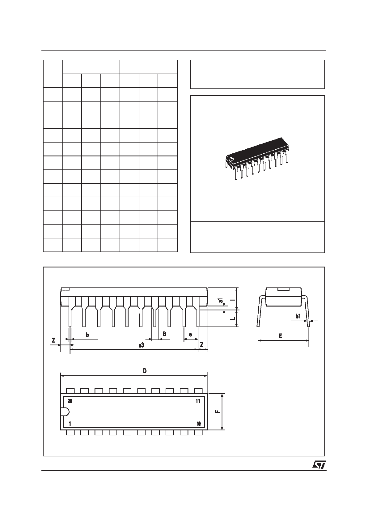
DIM.
MIN. TYP. MAX. MIN. TYP. MAX.
a1 0.254 0.010
B 1.39 1.65 0.055 0.065
b 0.45 0.018
b1 0.25 0.010
D 25.4 1.000
E 8.5 0.335
e 2.54 0.100
e3 22.86 0.900
F 7.1 0.280
I 3.93 0.155
L 3.3 0.130
Z 1.34 0.053
mm inch
OUTLINE AND
MECHANICAL DATA
DIP20
16/17

TDA7449
Information furnished is believed to be accurate and reliable. However, STMicroelectronics assumes no responsibility for the consequences
of use of such information nor for any infringement of patents or other rights of third parties which may result from its use. No license is
granted by implication or otherwise under any patent or patent rights of STMicroelectronics. Specification mentioned in this publication are
subject to change without notice. This publicationsupersedes and replaces all informationpreviously supplied. STMicroelectronics products
are not authorized for use as critical components in life support devices or systems without express written approval of STMicroelectronics.
Australia - Brazil - Canada- China - France - Germany - Italy - Japan - Korea - Malaysia - Malta - Mexico - Morocco - The Netherlands-
Singapore - Spain - Sweden- Switzerland - Taiwan - Thailand - UnitedKingdom - U.S.A.
The ST logo is a registered trademark of STMicroelectronics
1999STMicroelectronics – Printed in Italy– All Rights Reserved
STMicroelectronics GROUP OF COMPANIES
http://www.st.com
17/17
 Loading...